Bio-MEMS Technologies and Applications - Wang and Soper (Eds) Part 12 pptx
Bạn đang xem bản rút gọn của tài liệu. Xem và tải ngay bản đầy đủ của tài liệu tại đây (626.81 KB, 21 trang )
332 Bio-MEMS: Technologies and Applications
(a)
(b)
(c)
FIGURE 12.5
SEM photomicrographs of surface micromachined microneedles: (a) a metallic microneedle
with multiple output ports, (b) cross-section of the microneedle showing its microchannel, (c)
a sophisticatedly designed single microneedle with a shaft length of 500 µm.
DK532X_book.fm Page 332 Friday, November 10, 2006 3:31 PM
© 2007 by Taylor & Francis Group, LLC
MEMS for Drug Delivery 333
12.5 Out-of-Plane Silicon Microneedles
One of the major issues with respect to in-plane microneedles is their limited
density. This is due to the fact that only a one-dimensional array of micro-
needles can be microfabricated in a wafer. In order to achieve two-dimensional
arrays of microneedles, a complex microassembly process similar to one dem-
onstrated by Bai et al. [6] would be needed. With the typical microneedle inner
diameters of 10 to 100 µm, the limited density of the microneedles may become
an issue when delivering a large amount of a drug or in blood analysis appli-
cations, which typically require a fair amount of blood. In addition, shear stress
created by the tissue during insertion may cause mechanical fracture for the
single microneedle or one-dimensional array of long microneedles. The out-
of-plane microneedle array appears to be a viable option for addressing the
aforementioned issues because many microneedles can be microfabricated in
a wafer and the two-dimensional arrays are less prone to fracturing when
exposed to shear forces during penetration.
The first demonstrated out-of-plane microdevices for drug and gene deliv-
ery are sharp solid silicon structures [16,17]. Dizon et al. realized an array
of sharp solid silicon structures using a conventional anisotropic silicon wet
etching technique [16]. The timed wet etching using a square mask and fast-
etching (411) planes was used to realize approximately 80 µm high and very
sharp (with a tip radius of curvature less than 0.1 µm) solid silicon structures
has been coated with specific genes, which have been successfully transferred
(d)
FIGURE 12.5 (continued)
SEM photomicrographs of surface micromachined microneedles: (d) an array of the micro-
needles with a center-to-center distance of 2 mm. (From S. Chandrasekaran, J. Brazzle and
B. Frazier, J. of Microelectromechanical Systems, 12, 289–295, 2003, and S. Chandrasekaran and B.
Frazier, J. of Microelectromechanical Systems, 12, 281–288, 2003. With permission.)
DK532X_book.fm Page 333 Friday, November 10, 2006 3:31 PM
(Figure 12.6a). An array of such sharp solid silicon micropiercing structures
© 2007 by Taylor & Francis Group, LLC
MEMS for Drug Delivery 335
(a)
(b)
(c)
FIGURE 12.7
(a) Fabrication sequence, (b) SEM image of an array of pointed hollow silicon microneedles
with a height of 200 µm and a channel diameter of 40 µm, and (c) a conceptual schematic
diagram of a disposable MEMS syringe. (From B. Stoeber and D. Liepmann, Design, fabrication
and testing of a MEMS syringe, in Solid-State Sensors, Actuator and Microsystems Workshop, Hilton
Head Island, South Carolina, June 2–6, 2002. With permission.)
δ
Masks
Isotropic
etching
DRIE
(deep reactive
ion etching)
Flexible container
Drug
Needles
Skin
DK532X_book.fm Page 335 Friday, November 10, 2006 3:31 PM
© 2007 by Taylor & Francis Group, LLC
336 Bio-MEMS: Technologies and Applications
An array of needle channels through the substrate were defined using the
DRIE process, which was followed by an isotropic etching process with a
small offset of the center lines resulting in a microneedle with a sharp tip on
the circumference of its shaft. They further demonstrated a disposable
syringe that has a hollow microneedle array with a flexible polydimethyl
siloxane (PDMS) container for drug storage.
Griss and Stemme demonstrated an array of hollow, out-of-plane silicon
microneedles with openings in the shaft of the microneedles using three steps
of dry etching (Figure 12.8) [19]. This particular microneedle was developed with
FIGURE 12.8
(Top) Three-step fabrication sequence, (Bottom) SEM image of side-opened, out-of-plane hollow
silicon microneedles. (From P. Griss and G. Stemme, J. of Microelectromechanical Systems, 12,
296–301, 2003. With permission.)
Isotropic
DRIE
Anisotropic
DRIE
Isotropic
plasma
etch
(a)
(b)
(c)
Si
Si
Si
SiO
2
SiO
2
SiO
2
SiO
2
DK532X_book.fm Page 336 Friday, November 10, 2006 3:31 PM
© 2007 by Taylor & Francis Group, LLC
MEMS for Drug Delivery 337
a goal of achieving low flow resistance, high structural strength, a large area
of drug exposure to the tissue, and a low risk of clogging. The size and position
of the side flow channel openings were defined by RIE process parameters.
Gardeniers et al. demonstrated an array of hollow sharp silicon micro-
needles using a sequence of DRIE, anisotropic wet etching, and conformal
thin film deposition steps (Figure 12.9) [20]. The thick black line in the Figure
(a)
(b)
FIGURE 12.9
(a) Microneedle fabrication sequence; (b) SEM images of 350 µm–high triangular silicon mi-
croneedles. (From H. Gardeniers, R. Luttge, E. Berenschot, M. de Boer, S. Yeshurun, M. Hefetz,
R. Oever, and A. Berg, J. of Microelectromechanical Systems, 12, 855–862, 2003. With permission.)
ab
1
2
c
d
3
4
5
DK532X_book.fm Page 337 Friday, November 10, 2006 3:31 PM
© 2007 by Taylor & Francis Group, LLC
338 Bio-MEMS: Technologies and Applications
12.9a represents a silicon nitride coating, which is used as a protection layer
during KOH etching.
Mukerjee et al. produced different needle shapes by changing the relative
position of the central bore hole to the shaft of the microneedles by a com-
bination of DRIE, diamond blade circular sawing, and isotropic etching [21].
12.6 Out-of-Plane Metallic and Polymeric Microneedles
Along with out-of-plane silicon microneedles, there have been several inves-
tigations with respect to development of out-of-plane metallic microneedles
(c)
(d)
FIGURE 12.9 (continued)
(c,d) SEM images of 350 µm–high triangular silicon microneedles. (From H. Gardeniers, R.
Luttge, E. Berenschot, M. de Boer, S. Yeshurun, M. Hefetz, R. Oever, and A. Berg, J. of Micro-
electromechanical Systems, 12, 855–862, 2003. With permission.)
DK532X_book.fm Page 338 Friday, November 10, 2006 3:31 PM
© 2007 by Taylor & Francis Group, LLC
MEMS for Drug Delivery 339
using electroplated metals. McAllister et al. demonstrated three-dimensional
tapered-shaft and straight-shaft hollow metallic microneedles as shown in
Figure 12.10 [22]. The straight-shaft microneedles were fabricated by electro-
plating through cylindrically defined SU-8 holes. For the tapered needles, a
relatively complex combination of the SU-8 mold and the anisotropically
etched sharp solid Si mold insert [17] and electroplating technique were used.
The SU-8 was later etched from the top surface to form the tip opening by
O
2
/CHF
3
plasma and the SU-8 mold was fully etched away to release the
metallic microneedles. Similar tapered metallic microneedles were demon-
strated by Davis et al. using excimer and infrared laser micromachining [23].
In this approach, both the metal and polymer molds were drilled to form
tapered conical holes by controlling the energy distribution of the laser beam,
then conformal electroplating was carried out on these drilled molds to
fabricate the metallic microneedles.
(a)
(b)
FIGURE 12.10
SEM photomicrographs of metallic microneedle arrays: (a) NiFe microtubes 200 µm in height
and 80 and 40 µm in outer and inner diameter, respectively; (b) 150 µm–tall, hollow NiFe
microneedles using an SU-8 mold of a silicon mold insert. (From D. McAllister, F. Cros, S. Davis,
L. Matta, M. Prausnitz, M. Allen, Dig. Transducers’99, Int. Conf. Solid-State Sensors and Actuators,
1098–1101, 1999. With permission.)
DK532X_book.fm Page 339 Friday, November 10, 2006 3:31 PM
© 2007 by Taylor & Francis Group, LLC
340 Bio-MEMS: Technologies and Applications
Recently, Kim et al. demonstrated a tapered hollow metallic microneedle
array using a relatively simple backside exposure of the SU-8 process [24].
An SU-8 mesa was formed on a glass substrate and another SU-8 layer,
which was spun on top of the SU-8 mesa, was exposed through the backside
tures with angles between 3.1 and approximately 5° on top of the SU-8 mesa
was formed. Conformal electrodeposition of metal was carried out, followed
by mechanical polishing using a planarized polymeric layer. All organic
layers were then removed to create a metallic hollow microneedle array
with a fluidic reservoir on the back side. Both 200 µm– and 400 µm–tall, 10
by 10 arrays of metallic microneedles with inner diameters of the tip
between 33.6 and approximately 101 µm, and wall thicknesses of 10 to
approximately 20 µm were fabricated (Figure 12.11b). A polymeric microf-
luidic interconnector assembly was designed to have one male interconnec-
tor that directly fits into the fluidic reservoir (3 × 3 mm) of the microneedle
array at one end, and another male interconnector that provides external
fluidic interconnection to tubing (1/16 in. inner diameter) at the other end.
Liquid transfer testing was carried out (Figure 12.11c) and the measured
flow rate was approximately 72.5 nl/s-kPa.
As one of useful and cheap materials in MEMS applications, polymers
have also been utilized to fabricate three-dimensional microneedle arrays.
Moon and Lee demonstrated polymeric, hollow, out-of-plane microneedle
arrays using a modified LIGA process [25]. The fabrication process consists
of a vertical deep x-ray exposure and a successive inclined deep x-ray
triangular column array with a needle conduit through a deep x-ray mask.
The triangular column array is shaped into the microneedle array by the
second inclined x-ray exposure without additional mask alignment. Chang-
ing the inclined angle and the gap between the mask and PMMA (poly-
methyl-methacrylate) substrate, different types of microneedle arrays are
fabricated. Although the microneedle is made of PMMA, a polymer, the
three-dimensional tip is sharp, and mechanically robust enough to pierce
the skin without fracturing.
12.7 Mechanical Robustness of the Microneedles
Microneedles made of brittle materials such as silicon have a high risk of
catastrophic microneedle fracture during insertion. As an approach to solv-
ing this problem, Stupar and Pisano proposed parylene laminated silicon
needles, parylene needles, and parylene needles with silicon tips [26]. It was
found that fabricated parylene-coated silicon microneedles were strong
enough to withstand significant bending moments.
DK532X_book.fm Page 340 Friday, November 10, 2006 3:31 PM
of the glass substrate (Figure 12.11a). An array of SU-8 tapered pillar struc-
exposure, as shown in Figure 12.12. The first vertical exposure makes a
© 2007 by Taylor & Francis Group, LLC
MEMS for Drug Delivery 343
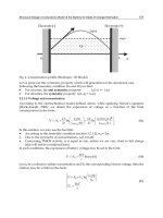
In order to predict the force of fracture of hollow microneedles, Kim et al.
developed analytic solutions of the critical buckling of arbitrarily angled,
truncated, hollow, cone-shaped columns (Figure 12.13) [24]. The critical buck-
ling load (P
cr
) for a fixed-free truncated cone column is given by:
, (12.1)
where d
0
and d
i
are outer and inner diameters of the cone column, α is the
taper angle, and L is the length of the microneedle. It was found that a single
400 µm–tall hollow cylindrical microneedle made of electroplated nickel with
a wall thickness of 20 µm, a tapered angle of 3.08°, and a tip inner diameter
of 33.6 µm has a critical buckling force of 1.8 N. This analytic solution can
be used to create square or rectangular cross-sectioned column structures
with proper modifications.
Recently, Davis et al. carried out comprehensive experimental and theo-
retical studies on the insertion and fracture forces of the microneedles [27].
It was found that insertion forces vary linearly with the interfacial area of
the needle tip. Measured insertion forces were low (0.1–3 N) enough so that
FIGURE 12.13
A schematic diagram of the hollow truncated cone column.
d
0
L
α
Z
d
1
P
E
L
dd d
cr
oi o
=
−
()
++
−
80
5
16
5
5
4
2
4
44 2 43
π
π
ππ
ddL
ddL
i
oi
3
242222
15
5
2
()
++
−
()
tan
tan
α
ππ α
++ − ++
−
()
120 30
5
2
24 33
ππ αddL
oi
tan
DK532X_book.fm Page 343 Friday, November 10, 2006 3:31 PM
© 2007 by Taylor & Francis Group, LLC
344 Bio-MEMS: Technologies and Applications
the microneedle can be inserted into the skin by hand. A thin-shelled ana-
lytical model was used in this study to predict the fracture force. As expected,
the fracture force was found to increase with increasing wall thickness, wall
angle, and needle tip radius.
12.8 Microreservoir Devices for Drug Delivery
Although the majority of the MEMS work on drug delivery is on the devel-
opment of microneedles, there has been another interesting approach for
drug delivery using MEMS technology. The device is called a microreservoir
and as the name suggests, it has a reservoir that contains a single dose of a
drug, and the reservoir is covered by a lid. Depending on the size, the device
can be surgically implanted, orally ingested, or injected into the body, and
the lid of the reservoir is broken in a controlled manner to release the desired
dosage of drug.
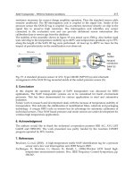
The first such device was reported by Santini et al. [28]. An array of microres-
ervoirs was defined by crystallographic anisotropic bulk micromachining of
silicon, and each microreservoir had a volume that could be filled with approx-
imately 25 nl of drug (Figure 12.14). The microreservoirs were sealed with a very
thin (0.3 µm–thick) gold membrane anode. When an appropriate electric poten-
tial is applied between the gold membrane anode and the cathode in the pres-
ence of chloride ion, the gold membrane is dissolved by its reaction with the
chloride ion by forming soluble gold–chloride complexes. Because the device is
scalable, large and small reservoirs with single or multiple drugs can be stored.
FIGURE 12.14
Silicon bulk micromachined microreservoir device for drug delivery. (From R. Shawgo, A.
Grayson, Y. Li, and M. Cima, Current Opinion in Solid State and Material Science, 6, 329–334, 2002.
With permission.)
DK532X_book.fm Page 344 Friday, November 10, 2006 3:31 PM
© 2007 by Taylor & Francis Group, LLC
MEMS for Drug Delivery 345
A good introductory article on the microreservoir drug delivery device
was published in an IEEE Spectrum [30]. When packaged with a power source
and control electronics, the device is the size of a pacemaker. The device can
be surgically implanted in the body and used for long-term controlled drug
release. Specific reservoirs can be manually opened on demand by an exter-
nal signal. It is also possible to make the microreservoir device ingestible;
each membrane has a different thickness to be dissolved sequentially so that
the drug can be released in a certain period of time.
A completely plastic microreservoir drug delivery system that does not
require an electrical power source was reported by Su and Lin [31]. The
device as shown in Figure 12.15 has an osmotic actuator on a substrate, which
is bonded with a patterned PDMS to form a reservoir, a microfluidic channel,
and a delivery port. Because this device uses water flow induced by osmosis
as actuation mechanism [32], it does not require electrical power source.
FIGURE 12.15
A water-powered drug delivery system. (From Y. Su and L. Lin, J. Microelectromechanical Systems,
13, 75–82, 2004. With permission.)
Drug reservoir
Drug flow
PDMS
microfluidic
components
Osmotic
microactuator
Water flow
Membrane
expansion
Osmotic
driving agent
Semipermeable
membrane
Structural
layer
Delivery
channel
Delivery port
Impermeable
membrane
DK532X_book.fm Page 345 Friday, November 10, 2006 3:31 PM
© 2007 by Taylor & Francis Group, LLC
346 Bio-MEMS: Technologies and Applications
Since the drug delivery rate and drug storage reservoir volume are control-
lable, this device can be used both for quick drug release as well as long-
term drug release.
12.9 Biocompatibility and Biofouling of MEMS Drug
Delivery Devices
Biocompatibility of materials used in devices for in vivo applications is of
paramount importance. Voskerician et al. carried out a comprehensive study
on the biocompatibility and biofouling of common materials used for MEMS
drug delivery devices including gold, silicon nitride, silicon dioxide, silicon,
and SU-8 photoresist [33]. The material under test was placed into a stainless
steel cage and the cage was implanted subcutaneously. The cage was peri-
odically checked, the exudates in the cage were sampled, and leukocyte
concentration was measured to determine the biocompatibility of the
implanted material. It was determined that the responses of all of these
materials, and that of the empty cage, were not much different, which let
us draw the conclusion that all of the tested materials are biocompatible.
In addition, in vivo biofouling, which is measured as an undesirable
accumulation of microorganisms on the implanted artificial surfaces, was
also studied by scanning electron micrography. It was determined that
gold, silicon nitride, silicon dioxide, and even SU-8 generate very low
accumulations of microorganisms. In fact, gold is biocompatible, less prone
to biofouling, and known for its corrosion resistance in many solutions
over the entire pH range, making it an ideal coating material for in vivo
MEMS devices.
However, silicon showed a much higher density of adherent cells in the
biofouling test. This result shows that drug delivery MEMS devices made
of silicon must be coated with biofouling-proof materials, such as silicon
dioxide or silicon nitride, to be used in in vivo applications.
References
[1] R. McGrew and M. McGrew, Encyclopedia of Medical History, McGraw Hill, New
York, 1985.
[2] J. Jagger, E. Hunt, J. Brand-Elnaggar, and R. Person, Rates of needle-stick injury
caused by various devices in a university hospital, New England J. of Medicine,
319, 284–288, 1988.
[3]
[4] K. Najafi and K. Wise, An implantable multielectrode array with on-chip signal
processing, IEEE J. Solid-State Circuits, 21, 1035–1044, 1986.
DK532X_book.fm Page 346 Friday, November 10, 2006 3:31 PM
Australian College of Dermatologists, .
© 2007 by Taylor & Francis Group, LLC
MEMS for Drug Delivery 347
[5] J. Chen, K. Wise, J. Hetke, and S. Bledsoe, A multichannel neural probe for
selective chemical delivery at the cellular level, IEEE Trans. Biomed. Eng., 44,
760–769, 1997.
[6] Q. Bai, K. Wise, and D. Anderson, A high-yield microassembly structure for
three dimensional microelectrode arrays, IEEE Trans. Biomed. Eng., 47, 281–289,
2000.
[7] L. Lin, A. Pisano, and R. Muller, Silicon processed microneedles, in Dig. Trans-
ducers’93, Int. Conf. Solid-State Sensors and Actuators, 237–240, 1993.
[8] L. Lin and A. Pisano, Silicon processed microneedles, J. Microelectromechanical
Systems, 8, 78–84, 1999.
[9] N. Talbot and A. Pisano, Polymolding: two wafer polysilicon micromolding of
closed flow passage for microneedles and microfluidic devices, Solid State Sen-
sor and Actuator Workshop Hilton Head, 265–268, 1998.
[10] J. Zahn, N. Talbot, D. Liepmann, and A. Pisano, Microfabricated polysilicon
microneedles for minimally invasive biomedical devices, Biomedical Microde-
vices, 2, 295–303, 2000.
[11] K. Chun, G. Hashiguchi, H. Toshioyoshi, B. Pioufle, J. Ishikawa, Y. Murakami,
E. Tamiya, Y. Kikuchi, and H. Fujita, DNA injection into cell conglomerates by
micromachined hollow microcapillary arrays, in Dig. Transducers’99, Int. Conf.
Solid-State Sensors and Actuators, 41–47, 1999.
[12] K. Oka, S. Aoyagi, Y. Arai, Y. Isono, G. Hashiguchi, and H. Fujita, Fabrication
of a microneedle for a trace blood test, Sensors and Actuators A, 97–98, 478–485,
2002.
[13] J. Brazzle, I. Papautsky, and B. Frazier, Hollow metallic micromachined needle
arrays, J. Micro Biomed. Devices, 2, 197–205, 2000.
[14] S. Chandrasekaran, J. Brazzle and B. Frazier, Surface micromachined metallic
microneedles, J. of Microelectromechanical Systems, 12, 289–295, 2003.
[15] S. Chandrasekaran and B. Frazier, Characterization of surface micromachined
metallic microneedles, J. of Microelectromechanical Systems, 12, 281–288, 2003.
[16] R. Dizon, H. Han, A. Russell, and M. Reed, An ion milling pattern transfer
technique for fabrication of three-dimensional micromechanical structures, J.
Microelectromech. Syst., 2, 151–159, 1993.
[17] S. Henry, D. McAllister, M. Allen, and M. Prausnitz, Microfabricated micron-
eedles: a novel approach to transdermal drug delivery, J. Pharm. Sci., 87,
922–925, 1998.
[18] B. Stoeber and D. Liepmann, Design, fabrication and testing of a MEMS syringe,
in Solid-State Sensors, Actuator and Microsystems Workshop, Hilton Head Island,
South Carolina, June 2–6, 2002.
[19] P. Griss and G. Stemme, Side-opened out-of-plane microneedles for microflu-
idic transdermal liquid transfer, J. of Microelectromechanical Systems, 12, 296–301,
2003.
[20] H. Gardeniers, R. Luttge, E. Berenschot, M. de Boer, S. Yeshurun, M. Hefetz,
R. Oever, and A. Berg, Silicon micromachined hollow microneedles for trans-
dermal liquid transport, J. of Microelectromechanical Systems, 12, 855–862, 2003.
[21] E. Mukerjee, S. Collins, R. Isseroff, and R. Smith, Microneedle array for trans-
dermal biological fluid extraction and in situ analysis, Sensors and Actuators, A,
114, 267–275, 2004.
[22] D. McAllister, F. Cros, S. Davis, L. Matta, M. Prausnitz, M. Allen, Three-dimen-
sional hollow microneedle and microtube arrays, in Dig. Transducers’99, Int.
Conf. Solid-State Sensors and Actuators, 1098–1101, 1999.
DK532X_book.fm Page 347 Friday, November 10, 2006 3:31 PM
© 2007 by Taylor & Francis Group, LLC
348 Bio-MEMS: Technologies and Applications
[23] S. Davis, M. Prausnitz, and M. Allen, Fabrication and characterization of laser
micromachined hollow microneedles, in Dig. Transducers’03, Int. Conf. Solid-
State Sensors and Actuators, 1435–1438, 2003.
[24] K. Kim, D. Park, H. Lu, K-H. Kim, JB Lee, A tapered hollow metallic micron-
eedle array using backside exposure of SU-8, J. Micromechanics and Microengi-
neering, 14, 597–603, 2004.
[25] S. Moon and S. Lee, A novel fabrication method of a microneedle array using
inclined deep x-ray exposure, J. Micromechanics and Microengineering, 15,
903–911, 2005.
[26] P. Stupar and A. Pisano, Silicon, parylene and silicon/parylene microneedles
for strength and toughness, in Dig. Transducers’01, Int. Conf. Solid-State Sensors
and Actuators, 1386, 2001.
[27] S. Davis, B. Landis, Z. Adams, M. Allen, and M. Prausnitz, Insertion of micron-
eedles into skin: measurement and prediction of insertion force and needle
fracture force, J. Biomechanics, 37, 1155–1163, 2004.
[28] J. Santini, M. Cima, and R. Langer, A controlled-release microchip, Nature, 397,
335–338, 1999.
[29] R. Shawgo, A. Grayson, Y. Li, and M. Cima, Bio-MEMS for drug delivery,
Current Opinion in Solid State and Material Science, 6, 329–334, 2002.
[30] C. Webb, Chip shots, IEEE Spectrum, 41, 48–53, 2004.
[31] Y. Su and L. Lin, A water-powered micro drug delivery system, J. Microelectro-
mechanical Systems, 13, 75–82, 2004.
[32] Y. Su, L. Lin, and A. Pisano, A water-powered osmotic microactuator, J. Micro-
electromechanical Systems, 11, 736–742, 2002.
[33] G. Voskerician, M. Shive, R. Shawgo, H. von Recum, J. Anderson, M. Cima,
and R. Langer, Biocompatibility and biofouling of MEMS drug delivery devic-
es, Biomaterials, 24, 1959–1967, 2003.
DK532X_book.fm Page 348 Friday, November 10, 2006 3:31 PM
© 2007 by Taylor & Francis Group, LLC
349
13
Microchip Capillary Electrophoresis Systems
for DNA Analysis
Ryan T. Kelly and Adam T. Woolley
CONTENTS
13.1 Introduction 349
13.2 Optimization of DNA Sequencing Separations 350
13.3 Parallel DNA Separations in Microchips 353
13.4 Integrated Microchips for DNA Analysis 356
13.5 Phase-Changing Sacrificial Layers for Polymer
Microchip Fabrication 357
13.6 Conclusions 359
Acknowledgment 360
References 360
13.1 Introduction
Nucleic acids are the storage medium for inherited information in living
organisms. Thus, scientists have considerable interest in developing
enhanced tools for the determination of nucleic acids, and the past twenty
years have seen a tremendous expansion in DNA analysis capabilities. Size
sorting of DNA, a critical aspect of both genotyping and sequencing, has
been transformed from an onerous, slow, and labor-intensive operation
involving slab gel electrophoresis to a rapid, automated, and ultra-high-
throughput process. The initial miniaturization of electrophoresis into a cap-
illary format enabled higher electric fields to be applied in DNA separations,
providing much faster analyses.
1–3
The subsequent development of capillary
array electrophoresis (CAE) systems with parallel bundles of lanes
4–6
pro-
vided a substantial boost in DNA sample analysis capacity. These advances
DK532X_book.fm Page 349 Friday, November 10, 2006 3:31 PM
© 2007 by Taylor & Francis Group, LLC
Microchip Capillary Electrophoresis Systems for DNA Analysis 351
Because DNA molecules have essentially the same electrophoretic mobility
in free solution regardless of fragment length, size-based separation is
achieved best in cross-linked gels or entangled polymer solutions. Entangled
linear polymers provide convenient sieving matrixes because they can be
pumped into capillaries or channels and replaced with fresh solution as
needed.
16
Linear polyacrylamide (LPA) has been widely used for DNA
sequencing in both capillaries
17
and microdevices, and extensive research
effort has led to improved microchip DNA separations with LPA. A system-
atic study was performed to develop a quantitative model of DNA separation
in LPA, resulting in nearly a threefold increase in sequencing read length
11
compared to earlier microchip results.
10
Another group used an optimized
polymerization protocol
17
to produce approximately 1 MDa average molec-
ular weight LPA, which provided four-color sequencing to 500 bases in 20 min
FIGURE 13.1
Schematic overview of typical methods for glass CE microchip fabrication. (a) A thin layer
of amorphous silicon (black) is deposited on a clean glass wafer (light gray, side view). (b)
Photoresist (dark gray) is spin coated on top of the amorphous silicon. (c) UV radiation on
regions of the surface that are not protected by a mask enables the patterned photoresist to
be solubilized in a developer solution. (d) Amorphous silicon, which is uncovered by the
removal of photoresist, is etched away in a CF
4
plasma. (e) The underlying glass in the pattern
of the exposure mask is etched isotropically in HF. (f) Photoresist and amorphous silicon are
removed from the etched wafer, which is then bonded in a furnace to another piece of glass.
(g) Electron micrograph of channels patterned and etched as described above. Scale bar is
50 µm. (Reprinted with permission from Simpson, P.C., Woolley, A.T., and Mathies, R.A., J.
Biomed. Microdevices, 1, 7, 1998. Copyright 1998, Springer Science and Business Media.) (h)
Top-view photograph of a 96-channel glass microdevice. (Image courtesy of Prof. Richard A.
Mathies.)
(d)
(c)
(b)
(a)
(e)
(f)
(h)
(g)
DK532X_book.fm Page 351 Friday, November 10, 2006 3:31 PM
© 2007 by Taylor & Francis Group, LLC
352 Bio-MEMS: Technologies and Applications
with 99.4% accuracy in a microchip.
15
Salas-Solano et al. used a mixture of
both high and low molecular weight LPA to improve microchip sequencing.
12
Similar read lengths were obtained using either 4% 10 MDa LPA or a blend
of 3% 10 MDa LPA and 1% 50 kDa LPA, but the run time was reduced
significantly with the mixed sieving matrix: four-color sequencing to 580
bases with 98.5% accuracy was achieved in 18 min.
12
A polyacrylamide nanogel medium with similar rheological properties to
LPA was developed to improve separation performance.
14
The matrix was
made by copolymerizing acrylamide with a small amount (approximately
10
–4
mol %) of N,N-methylene bisacrylamide (Bis) cross-linker, such that Bis
moieties were present in approximately 75% of the polymer chains, provid-
ing intra- and intermolecular covalent linkages. The Bis concentration was
sufficiently low to prevent the polymerization of a rigid, cross-linked hydro-
gel; instead, subcolloidal structures with an average radius of approximately
230 nm were formed. A comparison of performance between nanogel and
LPA matrixes using CE showed that average sequencing read lengths were
approximately 20% greater with the nanogel matrix, yielding 680 bases with
98.5% accuracy. The nanogel medium was also evaluated in 96-lane CAE
microdevices, and average sequence read lengths for the same separation
time increased by approximately 4% compared with LPA; importantly, load-
ing of the nanogel matrix into microchannels was much easier than LPA.
Other efforts to create sieving matrixes that are optimized for microchip
DNA separations have focused on reducing the solution viscosity because
the pressure (greater than 300 psi
13
) required for filling microchannels with
LPA can cause thermally bonded glass microdevices to delaminate.
16
One
promising approach is to use polymer solutions whose viscosities change
abruptly at a certain temperature, allowing easy pumping into channels in
the low viscosity state, after which the temperature can be adjusted to create
a solution with appropriate sieving properties for DNA separation. A copol-
ymer of N,N-diethylacrylamide and N,N-dimethylacrylamide was used as
such a thermoresponsive sieving medium for DNA sequencing.
18
The low-
viscosity solution was loaded into the separation column above 75°C, such
that the polymer chains were insoluble and aggregated to form dispersed,
colloidal droplets. For CE, the solution was cooled to 44°C, causing the
polymer to redissolve and form an entangled matrix. DNA sequence infor-
mation to approximately 460 bases was obtained with 97% accuracy in a CE
system. An alternative viscosity-switching matrix with a N-methoxyethyl-
acrylamide/N-ethoxyethylacrylamide copolymer has been reported, in
which the transition from low to high viscosity occurs when the temperature
is raised,
19
allowing facile solution pumping into a capillary at room tem-
perature. At 44°C (above the viscosity transition temperature), CE sequenc-
ing to approximately 600 bases with 98.5% accuracy was obtained. Even
though these viscosity-switching matrixes have only been evaluated in con-
ventional CE, their rheological properties are especially attractive for micro-
chip DNA separations.
DK532X_book.fm Page 352 Friday, November 10, 2006 3:31 PM
© 2007 by Taylor & Francis Group, LLC
354 Bio-MEMS: Technologies and Applications
HFE typing of 96 samples in about 8 min,
23
a severalfold improvement in
throughput over previous studies. However, increasing the number of separa-
tion lanes beyond approximately 50 would have been difficult in this format,
as the parallel bundle of capillaries in the detection region was already
approaching a 1 cm width, such that adding channels would have led to less
than ideal sampling in the linearly rastered scanning confocal detection system.
To overcome these limitations, a rotary scanning confocal detection setup
was constructed,
24
and radial CAE microplates were designed as outlined in
Figure 13.2.
25
These microchips had sample loading regions around the
FIGURE 13.2
Microdevice layout for 96-channel CAE sequencing. (a) Top view. (b) Vertical cutaway of a CAE
microdevice. Concentric plastic rings create separate “moats” used to provide electrical contact
to the drilled cathode and waste ports. (c) Expanded view of the injector region. (d) Expanded
view of the channel turn geometry used to reduce dispersion. (Reprinted with permission from
Paegel, B.M. et al., High throughput DNA sequencing with a microfabricated 96-lane capillary
array electrophoresis bioprocessor, Proc. Natl. Acad. Sci. USA, 99, 574, 2002. Copyright 2002,
National Academy of Sciences.)
Moat rings
Sample
(mm)
0
5
10
Cathode
Waste
(d)
(a)
(b)
(c)
DK532X_book.fm Page 354 Friday, November 10, 2006 3:31 PM
© 2007 by Taylor & Francis Group, LLC
Microchip Capillary Electrophoresis Systems for DNA Analysis 355
perimeter, and the separation capillaries converged at the center of a device
to enable the rotary detection system to probe each lane readily. Sequencing
separations on M13mp18 samples were carried out in 96-lane microplates,
with a mean read length of 430 bases per channel at 99% accuracy, corre-
sponding to a throughput of 1.7 kilobases per minute.
25
This sequencing rate
was fivefold higher than in the best commercial instrumentation and repre-
sented a 100-fold increase over the first microchip sequencing paper.
10
Radial
CAE microdevices for sizing 384 DNA specimens were also developed in a
layout similar to the 96-sample microplates.
26
These microsystems were fab-
ricated on 20 cm–diameter glass disks and had 8 cm–long, gel-filled channels.
HFE genotyping was performed simultaneously on 384 samples, and the
separation time was approximately 325 s, corresponding to a throughput of
more than one sample per second. This format provided faster separation
times and fourfold more lanes than the best commercial instruments, yield-
ing a 20-fold improvement in throughput.
As a summary of the enhanced throughput enabled by micromachining,
Figure 13.3 illustrates how sample processing rates have increased over the
past decade for DNA sizing and sequencing by microchip CE. Two key
advances led to improved DNA sequencing throughput: first, read lengths
increased fourfold between 1995 and 1999 with better sieving matrix formu-
lations and optimized separation conditions (discussed in Section 13.2); sec-
ond, multichannel sequencing microchips raised sample throughput from
one lane in 1995,
10
to 16 lanes in 2000,
27
and 96 lanes in 2002.
25
Is it possible
to increase DNA throughput in CE microdevices even more? Several factors
influence how many samples can be analyzed in CE microchips. These lim-
itations include the microdevice surface area occupied by sample input sys-
tems, the length of separation channels, and the parallel bundling of lanes
for detection. For instance, in 20 cm–diameter, 384-lane microplates, approx-
imately 15% of the surface area was occupied by the sample injectors alone.
26
Thus, increasing well beyond several hundred capillaries would require
either larger-diameter substrates or microfabrication advances that reduce
sample injector dimensions. Moreover, the packing of lanes in the central
FIGURE 13.3
Throughput improvement over time for DNA analysis in micromachined systems. Circles refer
to DNA sizing (left axis) and are from References 9, 21, 23, 24, and 26. Diamonds correspond
to four-color sequencing (right axis) and are from References 10, 15, 25, 27, and 52.
100
10000
1000
100
10
Bases/minute
1
10
Samples/minute
1
0.1
1992 1994 1996 1998
Year
2000 2002 2004
DK532X_book.fm Page 355 Friday, November 10, 2006 3:31 PM
© 2007 by Taylor & Francis Group, LLC
358 Bio-MEMS: Technologies and Applications
be sustained in glass (approximately 2,000 psi),
48
making it difficult to fill
thermally bonded polymer devices with viscous sieving solutions typically
used for DNA sequencing. Second, covalent surface passivation procedures
are straightforward for glass microdevices, but less well established in poly-
mers. Therefore, polymer microchips with a stronger bond between sub-
strates and appropriately modified surfaces should perform as well as glass,
while offering greater fabrication ease and lower costs.
We have addressed the delamination issue by developing a phase-chang-
ing sacrificial layer (PCSL) approach for solvent bonding polymer substrates
that can withstand much higher internal pressures than thermally sealed
systems.
47
poly(dimethylsiloxane) (PDMS, gray
, Figure 13.4a) over a patterned PMMA
substrate (white), with access holes in the PDMS aligned with the PMMA
channel ends. The assembly is heated to 70°C, and a liquid PCSL (paraffin
wax, white with gray horizontal lines, Figure 13.4b) is loaded into the
microchannels. When the device is cooled to room temperature, the PCSL
solidifies (gray with white horizontal lines, Figure 13.4c) and prevents bond-
ing solvent (black) or softened PMMA from filling the channels during the
process of affixing a polymer cover plate to the patterned substrate (Figure
13.4d). Once a seal has formed between the PMMA pieces, the microchip
is heated to 70°C to melt the PCSL, which is removed easily (Figure 13.4e)
by first applying vacuum at the reservoirs and then flushing cyclohexane
through the channels. The improved robustness of PCSL-fabricated, solvent-
bonded PMMA microdevices has allowed hundreds of CE separations at
electric fields as high as 1.5 kV/cm to be performed in a single microchip
without any degradation of performance.
47
Moreover, internal pressures
greater than 2,200 psi have been applied without delaminating the PMMA
substrates,
47
indicating excellent compatibility with conditions for introduc-
ing viscous sieving media for DNA sequencing.
In addition, PCSLs can facilitate the interfacing of hydrogel membranes with
microfluidic networks in polymers.
49
This capability should be valuable for
DNA sample enrichment prior to CE, which has been shown in glass microde-
vices having a porous sodium silicate thin film,
50,51
although the microchip
fabrication was somewhat cumbersome. In contrast, polymerization of an ion-
permeable membrane in situ using a PCSL is straightforward; a patterned
microchannel is filled with PCSL (Figure 13.4a and b) as described above, and
a second substrate having an opening to serve as a membrane reservoir is
brought into contact with the microchannel-containing piece (Figure 13.4f).
The PCSL prevents the prepolymer solution (dark gray, Figure 13.4g) in the
well from filling the channel, and after polymerization a rigid, semipermeable
hydrogel (gray with white cross-hatching, Figure 13.4h) is formed. Finally, the
PCSL is melted and removed (Figure 13.4i) as described previously, providing
a microfluidic array interfaced with an ionically conductive hydrogel.
DK532X_book.fm Page 358 Friday, November 10, 2006 3:31 PM
The solvent bonding fabrication procedure is shown in Figure
13.4a–e. First, temporarily enclosed microchannels are formed by sealing
© 2007 by Taylor & Francis Group, LLC
Microchip Capillary Electrophoresis Systems for DNA Analysis 361
18. Buchholz, B.A. et al., Microchannel DNA sequencing matrices with a thermally
controlled "viscosity switch," Anal. Chem., 73, 157, 2001.
19. Kan, C W., Doherty, E.A.S., and Barron, A.E., A novel thermogelling matrix
for microchannel DNA sequencing based on poly-N-alkoxyacrylamide copol-
ymers, Electrophoresis, 24, 4161, 2003.
20. Jacobson, S.C. et al., Microchip structures for submillisecond electrophoresis,
Anal. Chem., 70, 3476, 1998.
21. Woolley, A.T., Sensabaugh, G.F., and Mathies, R.A., High-speed DNA genotyp-
ing using microfabricated capillary array electrophoresis chips, Anal. Chem.,
69, 2181, 1997.
22. Simpson, P.C., Woolley, A.T., and Mathies, R.A., Microfabrication technology
for the production of capillary array electrophoresis chips, J. Biomed. Microde-
vices, 1, 7, 1998.
23. Simpson, P.C. et al., High throughput genetic analysis using microfabricated
96-sample capillary array electrophoresis microplates, Proc. Natl. Acad. Sci.
USA, 95, 2256, 1998.
24. Shi, Y. et al., Radial capillary array electrophoresis microplate and scanner for
high-performance nucleic acid analysis, Anal. Chem., 71, 5354, 1999.
25. Paegel, B.M. et al., High throughput DNA sequencing with a microfabricated
96-lane capillary array electrophoresis bioprocessor, Proc. Natl. Acad. Sci. USA,
99, 574, 2002.
26. Emrich, C.A. et al., Microfabricated 384-lane capillary array electrophoresis bio-
analyzer for ultrahigh-throughput genetic analysis, Anal. Chem., 74, 5076, 2002.
27. Liu, S. et al., Automated parallel DNA sequencing on multiple channel micro-
chips, Proc. Natl. Acad. Sci. USA, 97, 5369, 2000.
28. Waters, L.C. et al., Multiple sample PCR amplification and electrophoretic
analysis on a microchip, Anal. Chem., 70, 5172, 1998.
29. Woolley, A.T. et al., Functional integration of PCR amplification and capillary
electrophoresis in a microfabricated DNA analysis device, Anal. Chem., 68,
4081, 1996.
30. Giordano, B.C. et al., Polymerase chain reaction in polymeric microchips: DNA
amplification in less than 240 seconds, Anal. Biochem., 291, 124, 2001.
31. Ferrance, J.P. et al., Developments toward a complete micro-total analysis
system for Duchenne muscular dystrophy diagnosis, Anal. Chim. Acta, 500,
223, 2003.
32. Lagally, E.T., Emrich, C.A., and Mathies, R.A., Fully integrated PCR-capillary
electrophoresis microsystem for DNA analysis, Lab Chip, 1, 102, 2001.
33. Lagally, E.T., Medintz, I., and Mathies, R.A., Single-molecule DNA amplifica-
tion and analysis in an integrated microfluidic device, Anal. Chem., 73, 565, 2001.
34. Kopp, M.U., de Mello, A.J., and Manz, A., Chemical amplification: Continuous-
flow PCR on a chip, Science, 280, 1046, 1998.
35. Krishnan, N. et al., Reactions and fluidics in miniaturized natural convection
systems, Anal. Chem., 76, 6254, 2004.
36. Chen, J.F. et al., Electrokinetically synchronized polymerase chain reaction
microchip fabricated in polycarbonate, Anal. Chem., 77, 658, 2005.
37. Breadmore, M.C. et al., Microchip-based purification of DNA from biological
samples, Anal. Chem., 75, 1880, 2003.
38. Olsen, K.G., Ross, D.J., and Tarlov, M.J., Immobilization of DNA hydrogel plugs
in microfluidic channels, Anal. Chem., 74, 1436, 2002.
DK532X_book.fm Page 361 Friday, November 10, 2006 3:31 PM
© 2007 by Taylor & Francis Group, LLC