The MEMS Handbook (1st Ed) - M. Gad el Hak Part 8 ppt
Bạn đang xem bản rút gọn của tài liệu. Xem và tải ngay bản đầy đủ của tài liệu tại đây (118.28 KB, 3 trang )
© 2002 by CRC Press LLC
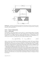
16.8.3 Corner Compensation
16.8.3.1 Underetching
Underetching of a mask which contains no convex corners, i.e., corners turning outside in, in principle
stems from mask misalignment and/or from a finite etching of the {111} planes. Peeters measured
the widening of {111}-walled V-grooves in a (100) Si wafer after etching in 7 M KOH at 80 ± 1° over
24 hours as 9 ± 0.5
µm [Peeters, 1994]. The sidewall slopes of the V-groove are a well-defined 54.74°,
and the actual etch rate R
111
is related to the rate of V-groove widening R
v
through:
(16.41)
with R
111
the etch rate in nm/min and R
v
the groove widening, also in nm/min. The V-groove widening
experiment then results in a R
111
of 2.55 ± 0.15 nm/min. In practice, this etch rate implies a mask
underetching of only 0.9
µm for an etch depth of 360 µm. For a 1-mm-long V-groove and a 1° misalign-
ment angle, a total underetching of 18
µm is theoretically expected, with 95% due to misalignment and
only 5% due to etching of the {111} sidewalls [Peeters, 1994]. The total underetching will almost always
be determined by misalignment, rather than by etching of {111} walls.
Mask underetching with masks that do include convex corners is usually much larger than the underetch-
ing just described, as the etchant tends to circumscribe the mask opening with {111} walled cavities. This
is usually called undercutting rather than underetching. It is advisable to avoid mask layouts with convex
corners. Often mesa-type structures are essential, though, and in that case there are two possible ways to
reduce the undercutting. One is by chemical additives, reducing the undercut at the expense of a reduced
anisotropy ratio, and the other is by a special mask compensating the undercut at the expense of more
lost real estate.
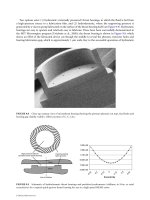
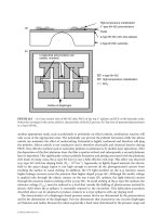
FIGURE 16.59 Comparison of conventional and SFB processes. The SFB process results in a chip which is at least
50% smaller than the conventional chip. (From Bryzek, J. et al., Silicon Sensors and Microstructures, Novasensor,
Fremont, CA, 1990. With permission.)
R
111
1
2
(54.74°)R
v
or R
111
sin 0.408 R
v
⋅==
© 2002 by CRC Press LLC
16.8.3 Corner Compensation
16.8.3.1 Underetching
Underetching of a mask which contains no convex corners, i.e., corners turning outside in, in principle
stems from mask misalignment and/or from a finite etching of the {111} planes. Peeters measured
the widening of {111}-walled V-grooves in a (100) Si wafer after etching in 7 M KOH at 80 ± 1° over
24 hours as 9 ± 0.5
µm [Peeters, 1994]. The sidewall slopes of the V-groove are a well-defined 54.74°,
and the actual etch rate R
111
is related to the rate of V-groove widening R
v
through:
(16.41)
with R
111
the etch rate in nm/min and R
v
the groove widening, also in nm/min. The V-groove widening
experiment then results in a R
111
of 2.55 ± 0.15 nm/min. In practice, this etch rate implies a mask
underetching of only 0.9
µm for an etch depth of 360 µm. For a 1-mm-long V-groove and a 1° misalign-
ment angle, a total underetching of 18
µm is theoretically expected, with 95% due to misalignment and
only 5% due to etching of the {111} sidewalls [Peeters, 1994]. The total underetching will almost always
be determined by misalignment, rather than by etching of {111} walls.
Mask underetching with masks that do include convex corners is usually much larger than the underetch-
ing just described, as the etchant tends to circumscribe the mask opening with {111} walled cavities. This
is usually called undercutting rather than underetching. It is advisable to avoid mask layouts with convex
corners. Often mesa-type structures are essential, though, and in that case there are two possible ways to
reduce the undercutting. One is by chemical additives, reducing the undercut at the expense of a reduced
anisotropy ratio, and the other is by a special mask compensating the undercut at the expense of more
lost real estate.
FIGURE 16.59 Comparison of conventional and SFB processes. The SFB process results in a chip which is at least
50% smaller than the conventional chip. (From Bryzek, J. et al., Silicon Sensors and Microstructures, Novasensor,
Fremont, CA, 1990. With permission.)
R
111
1
2
(54.74°)R
v
or R
111
sin 0.408 R
v
⋅==
© 2002 by CRC Press LLC
planes was confirmed by Seidel (1986); at the wafer surface, the sectional line of a (411) and a (111)
plane point in the <410> direction, forming an angle of 30.96
°
with the <110> direction, and it was in
this direction that he found a maximum in the etch rate. In KOH and EDP etchants Bean (1978) identified
the fast undercutting planes as {331} planes. Puers and Sansen (1990), for alkali/alcohol/water, identified
the fast underetching planes as {331} planes, as well. Mayer et al. (1990), working with pure KOH, could
not confirm the occurrence of such planes. Lee indicated that in hydrazine-water the fastest underetching
planes are {211} planes [Lee, 1969]. Abu-Zeid (1984) reported that the main beveling planes are {212}
planes in ethylene-diamine-water solution (no added pyrocatechol). Wv and Ko (1989) found the main
beveling planes at undercut corners to be {212} planes whether using KOH, hydrazine, or EPW solutions
are used. In view of our earlier remarks on the sensitivity of etching rates of higher index rates on a wide
variety of parameters (temperature, concentration, etching size, stirring, cation effect, alcohol addition,
complexing agent, etc.) these contradictory results are not too surprising. Along the same line, Wu and
Ko (1989) and Peurs et al. (1990) have suggested triangles to compensate for underetching, but Mayer
et al. (1997) found them to lead to rugged surfaces at the convex corner. Combining a chemical etchant
with more limited undercutting (IPA in KOH) with Sandmaier’s reduced compensation structure schemes
could further decrease the required size of the compensation features while retaining an acceptable
anisotropy.
Corner compensation for <110>-oriented Si was explored by Ciarlo [1987]. Ciarlo comments that
both corner compensation and corner rounding can be minimized by etching from both surfaces so as
to minimize the etch time required to achieve the desired features. This requires accurate front-to-back
alignment and double-sided polished wafers.
Employing corner compensation offers access to completely new applications such as rectangular
solids, orbiting V-grooves, truncated pyramids with low cross-sections on the wafer surface, bellow
structures for decoupling mechanical stresses between micromechanical devices and their packaging, etc.
[Sandmaier et al., 1991].
16.9 Wet Bulk Micromachining Examples
Example 1. Dissolved Wafer Process
Figure 16.65 illustrates the dissolved wafer process Cho is optimizing for the commercial production
of low-cost inertial instruments [Cho, 1995]. This process, also in use by Draper Laboratory [Greiff,
1995; Weinberg et al., 1996] for the same application, involves a sandwich of a silicon sensor anodically
bonded to a glass substrate. The preparation of the silicon part requires only two masks and three
processing steps. A recess is KOH-etched into a p-type (100) silicon wafer (step 1 with mask 1), followed
by a high-temperature boron diffusion (step 2 with no mask). In step one RIE may be used as well.
Cho claims that by maintaining a high-temperature uniformity in the KOH etching bath (
±
0.1
°
C),
the accuracy and absolute variation of the etch across the wafer, wafer-to-wafer, and lot-to-lot, can be
maintained to
<
0.1
µ
m using pre-mixed, 45 wt% KOH. Cho is also using low-defect oxidation techniques
(e.g., nitrogen annealing and dry oxidation) to form defect-free silicon surfaces. In the boron diffusion
the key is optimizing the oxygen content. In general, the optimal flow of oxygen is on the order of 3 to
5% of the nitrogen flow, in which case the doping uniformity is on the order of
±
0.2
µ
m. Varying the
KOH etch depth and the shallow boron diffusion time, a wide variety of operating ranges and
sensitivities for sensors can be obtained. Next, the silicon is patterned for a reactive ion etching (RIE)
etch (step 3 with mask 2). Aspect ratios above 10 are accessible. Using some of the newest dry etching
techniques depths in excess of 500
µ
m at rates above 4
µ
m/min (with a SF
6
chemistry) are now possible
[Craven and Pandhumsporn, 1995]. The glass substrate (#7740 Corning glass) preparation involves
etching a recess, depositing and in a one-mask step patterning a multi-metal system of Ti/Pt/Au. The
electrostatic bonding of glass to silicon takes place at 335
°
C with a potential of 1000 V applied between
the two parts (electrostatic or anodic bonding is explained in detail in Madou [1997, chap. 8]).
Commercial bonders have alignment accuracies on the order of <1
µ
m. The lightly doped silicon is
dissolved in an EDP solution at 95
°
C. The keys to uniform EDP etching are temperature uniformity