The MEMS Handbook (1st Ed) - M. Gad el Hak Part 11 doc
Bạn đang xem bản rút gọn của tài liệu. Xem và tải ngay bản đầy đủ của tài liệu tại đây (216.2 KB, 5 trang )
© 2002 by CRC Press LLC
another appropriate mask, such as polyimide or polyimide on silicon nitride, anodization reaction will
only occur at the appropriate areas. The polyimide can prevent the pinhole formation while the silicon
nitride can minimize the effect of undercutting. Polyimide is highly conformal and therefore will plug
the pinholes. Silicon nitride is not conductive and is therefore electrically and chemical inactive during
PECE. One effective method used to neutralize pinholes in platinum is by double-layer deposition. After
the deposition of the first platinum layer, the film is sputter-etched, and subsequently a second platinum
layer is deposited. This significantly reduces pinhole formation and pitting associated with the platinum
etch mask. In many cases, the p-type SiC layer is not a fully effective etch-stop. This effect was observed
in p-type SiC with low doping levels (N
a
∼
10
18
cm
−
3
). Apparently, in lightly doped material, the electric
field in the space-charge region is not high enough to prevent all the photogenerated carriers from
reaching the surface to cause etching. In addition, the UV light incident on the n–p junction causes
higher leakage currents across the junction than higher doped p-type SiC. Although the anodic voltage
is applied only through the ohmic contact on the top n-type SiC epilayer, the light-induced current
through the junction leads to etching of the p-type SiC. To avoid etching of the p-type SiC epilayer, the
reference voltage (V
SCE
) must be reduced to a level that curtails the drifting of photocarriers assisted by
electric field when the p-epilayer is eventually exposed to the electrolyte. This fabrication procedure
described above can be adopted to produce resistors in n-type epilayers with any doping level.
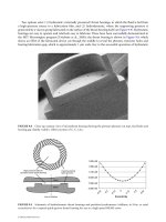
The characteristics of a diaphragm-based pressure sensor device are determined by the piezoresistors
and by the dimensions of the diaphragm. Two key dimensions that characterize any circular diaphragm
are thickness and radius. Because the radius is generally a fixed value determined by the pressure range and
FIGURE 20.3
(a) Cross-section view of 6H-SiC after PECS of the top n
+
-epilayer and ECE of the backside cavity.
Notice the curvature in the cavity, which is characteristic of the ECE process. (b) Top view of patterned piezoresistors
in n-type 6H-SiC.
p-type 6H-SiC etch-stop epilayer
n
+
-type 6H-SiC piezoresistors
n-type 6H-SiC substrate
High-temperature metallization
Oxide
(a)
© 2002 by CRC Press LLC
another appropriate mask, such as polyimide or polyimide on silicon nitride, anodization reaction will
only occur at the appropriate areas. The polyimide can prevent the pinhole formation while the silicon
nitride can minimize the effect of undercutting. Polyimide is highly conformal and therefore will plug
the pinholes. Silicon nitride is not conductive and is therefore electrically and chemical inactive during
PECE. One effective method used to neutralize pinholes in platinum is by double-layer deposition. After
the deposition of the first platinum layer, the film is sputter-etched, and subsequently a second platinum
layer is deposited. This significantly reduces pinhole formation and pitting associated with the platinum
etch mask. In many cases, the p-type SiC layer is not a fully effective etch-stop. This effect was observed
in p-type SiC with low doping levels (N
a
∼
10
18
cm
−
3
). Apparently, in lightly doped material, the electric
field in the space-charge region is not high enough to prevent all the photogenerated carriers from
reaching the surface to cause etching. In addition, the UV light incident on the n–p junction causes
higher leakage currents across the junction than higher doped p-type SiC. Although the anodic voltage
is applied only through the ohmic contact on the top n-type SiC epilayer, the light-induced current
through the junction leads to etching of the p-type SiC. To avoid etching of the p-type SiC epilayer, the
reference voltage (V
SCE
) must be reduced to a level that curtails the drifting of photocarriers assisted by
electric field when the p-epilayer is eventually exposed to the electrolyte. This fabrication procedure
described above can be adopted to produce resistors in n-type epilayers with any doping level.
The characteristics of a diaphragm-based pressure sensor device are determined by the piezoresistors
and by the dimensions of the diaphragm. Two key dimensions that characterize any circular diaphragm
are thickness and radius. Because the radius is generally a fixed value determined by the pressure range and
FIGURE 20.3
(a) Cross-section view of 6H-SiC after PECS of the top n
+
-epilayer and ECE of the backside cavity.
Notice the curvature in the cavity, which is characteristic of the ECE process. (b) Top view of patterned piezoresistors
in n-type 6H-SiC.
p-type 6H-SiC etch-stop epilayer
n
+
-type 6H-SiC piezoresistors
n-type 6H-SiC substrate
High-temperature metallization
Oxide
(a)
© 2002 by CRC Press LLC
21
Deep Reactive Ion
Etching for Bulk
Micromachining
of Silicon Carbide
21.1 Introduction
21.2 Fundamentals of High-Density Plasma Etching
21.3 Fundamentals of SiC Etching Using
Fluorine Plasmas
21.4 Applications of SiC DRIE: Review
21.5 Applications of SiC DRIE: Experimental Results
21.6 Applications of SiC DRIE: Fabrication
of a Bulk Micromachined SiC Pressure Sensor
21.7 Summary
21.1 Introduction
It is often desired to insert microsensors and other microelectromechanical systems (MEMS) into harsh
(e.g., hot or corrosive) environments. Silicon carbide (SiC) offers considerable promise for such appli-
cations, because SiC can be used to fabricate both high-temperature electronics and extremely durable
microstructures. One of the attractive characteristics of SiC is the compatibility of its process technologies
with those of silicon, which allows for the co-fabrication of SiC and silicon MEMS. However, a very
important difference in the processing of these semiconductors arises from the chemical inertness of SiC,
a characteristic that makes it attractive for use in corrosive environments but also makes it very difficult
to micromachine.
Realization of the full potential of SiC MEMS will require the development of a set of micromachining
tools for SiC comparable to the tool set available for silicon. Micromachining methods are generally
classified as bulk, in which the wafer is etched, or surface, in which deposited surface layers are patterned.
Surface micromachining methods for deposited SiC layers have been developed to a high level [Mehregany
et al., 1998]. Silicon carbide can be readily etched to the required depths of just several microns using
reactive ion etching (RIE) processes [Yih et al., 1997]. Further work remains to be done, however, in
developing RIE processes with greater selectivity for SiC. Current RIE processes lack the selectivity
needed to etch a SiC layer entirely through while minimally modifying an underlying silicon or silicon
dioxide layer. This limitation has motivated the development of a micromolding method in which SiC
is deposited into molds formed by RIE of silicon or silicon dioxide [Yasseen et al., 1999].
The emphasis here is bulk micromachining of SiC, for the fabrication of SiC microstructures with
vertical dimensions from approximately 10
µ
m to several hundred microns. Three methods for bulk
Glenn M. Beheim
NASA Glenn Research Center
© 2002 by CRC Press LLC
22
Microfabricated
Chemical Sensors for
Aerospace Applications
22.1 Introduction
22.2 Aerospace Applications
Leak Detection • Fire Safety Monitoring • Engine
Emission Monitoring
22.3 Sensor FabricationTechnologies
Microfabrication and Micromachining
Technology • Nanomaterials • SiC-Based
High-Temperature Electronics
22.4 Chemical Sensor Development
Si-Based Hydrogen Sensor Technology • Nanocrystalline
Tin Oxide Thin Films for NO
x
and CO
Detection • Electrochemical Cell Oxygen Detection • SiC-
Based Hydrogen and Hydrocarbon Detection • NASICON-
Based CO
2
Detection
22.5 Future Directions, Sensor Arrays
and Commercialization
High-Selectivity Gas Sensors Based on Ceramic
Membranes • Leak-Detection Array • High-Temperature
Electronic Nose
22.6 Commercial Applications
22.7 Summary
Acknowledgments
22.1 Introduction
The advent of microelectromechanical systems (MEMS) technology is important in the development
and use of chemical sensor technology for a range of applications, especially those that include operation
in harsh environments or effect safety. As will be discussed in this chapter, chemical microsensors can
provide unique information that can significantly improve safety and reliability while decreasing costs
of a system or process. Such information can also be used to improve a system’s performance and reduce
its effect on the environment. Chemical sensor data also can complement data derived from physical
measurements such as temperature, pressure, heat flux etc., further improving overall knowledge of a
system and expanding its capabilities.
However, the application of even traditional macrosized chemical sensor technology can be problematic.
Chemical sensors often need to be specifically designed (or tailored) to operate in a given environment.
It is often the case that a chemical sensor that meets the needs of one application will not function
Gary W. Hunter
NASA Glenn Research Center
Chung-Chiun Liu
Case Western Reserve University
Darby B. Makel
Makel Engineering, Inc.
© 2002 by CRC Press LLC
23
Packaging of
Harsh-Environment
MEMS Devices
23.1 Introduction
23.2 Material Requirements for Packaging
Harsh-Environment MEMS
Substrates • Metallization/Electrical Interconnection
System • Die-Attach • Hermetic Sealing
23.3 High-Temperature Electrical Interconnection
System
Thick-Film Metallization • Thick-Film-Based
Wirebond • Conductive Die-Attach
23.4 Thermomechanical Properties of Die-Attach
Governing Equations and Material
Properties • Thermomechanical Simulation of Die-Attach
23.5 Discussion
Innovative Materials • Innovative Structures • Innovative
Processes
Acknowledgments
23.1 Introduction
Microelectromechanical system (MEMS) devices, as they are defined, are both electrical and mechanical
devices. Via microlevel mechanical operation, MEMS devices, as sensors, transform mechanical, chem-
ical, optical, magnetic and other nonelectrical parameters to electrical/electronic signals; as actuators,
MEMS devices transform electrical/electronic signal to nonelectrical/electronic operations. Therefore,
MEMS devices very often interact with the environment electrically, magnetically, optically, chemically
and mechanically. In order to support these nonconventional device operations (i.e., the device mechan-
ical operation and the nonelectrical interactions between the device and their environments), new
packaging capabilities beyond those provided by conventional integrated circuit (IC) packaging technol-
ogy are required [Madou, 1997]. A chemically inert, optically dark and electromagnetically “quiet”
environment for packaging conventional ICs, provided by hermetic sealing and electromagnetic screen-
ing, is no longer suitable for packaging most MEMS devices. Because MEMS devices have very specific
requirements for their immediate packaging environment, it is expected that the design of MEMS
packaging will be very device dependent. This is in contradiction to the conventional IC packaging
practice in which a universal package design can accommodate many different ICs. Compared to con-
ventional IC packaging, the most distinct issue of MEMS packaging is to meet the requirements imposed
by the mechanical operability and reliability of MEMS devices.
Liang-Yu Chen
NASA Glenn Research Center
Jih-Fen Lei
NASA Glenn Research Center