The MEMS Handbook Introduction & Fundamentals (2nd Ed) - M. Gad el Hak Part 2 doc
Bạn đang xem bản rút gọn của tài liệu. Xem và tải ngay bản đầy đủ của tài liệu tại đây (1.65 MB, 30 trang )
could be rotated about an axis perpendicular to the grid. This caused all of the specimens to buckle, each
a different amount than its neighbor. When the grip moved, each specimen in turn was straightened and
pulled. The recorded force-displacement record enabled measurement of modulus and strength.
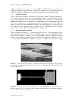
3.3.5.1 Specimen in Frame
Read and Dally (1992) introduced a very effective way of handling thin-film specimens in 1992. The ten-
sile specimen is patterned onto the surface of a wafer, and then a window is etched in the back of the wafer
to expose the gauge section. The result is a specimen suspended across a rectangular frame, which can be
handled easily and placed into a test machine. The two larger ends of the frame are fastened to grips, and
the two narrower sides are cut to completely free the specimen. This is an extension of the much earlier
approach by Neugebauer (1960) and has been adopted by others [Cunningham et al., 1995; Emery et al.,
1997; Ogawa et al., 1997; Sharpe et al., 1997c; Cornella et al., 1998; Yi and Kim, 1999b]. A SEM photo-
graph of such a specimen while still in the frame is shown in Figure 3.2.
3.3.5.2 Specimen Fixed at One End
Tsuchiya introduced the concept of a tensile specimen fixed to the die at one end and gripped with an
electrostatic probe at the other end [Tsuchiya et al., 1998]. This approach has been adopted by this author
and his students [Sharpe et al., 1998a]; Figure 3.3 is a photograph of this type of specimen. The gauge
section is 3.5 µm thick, 50 µm wide, and 2 mm long. The fixed end is topped with a gold layer for electri-
cal contact. The grip end is filled with etch holes, as are the two curved transition regions from the grips
Mechanical Properties of MEMS Materials 3-7
35x
285 µm
FIGURE 3.2 Scanning electron micrograph of a polysilicon tensile specimen in a supporting single-crystal silicon
frame. (Reprinted with permission from Sharpe, W.N., Jr., Yuan, B., Vaidyanathan, R., and Edwards, R.L. [1996]
Proc. SPIE 2880, pp. 78–91.)
FIGURE 3.3 A tensile specimen fixed at the left end with a free grip end at the right end. (Reprinted with permis-
sion from Sharpe, W.N., Jr., and Jackson, K. [2000] Microscale Systems: Mechanics and Measurements Symposium,
Society for Experimental Mechanics, pp. ix–xiv.)
© 2006 by Taylor & Francis Group, LLC
to the gauge section. The large grip end is held in place during the etch-release process by four anchor
straps, which are broken before testing.
Chasiotis and Knauss (2000) have developed procedures for gluing the grip end of a similar specimen
to a force/displacement transducer, which enables application of larger forces. A different approach is to
fabricate the grip end in the shape of a ring and insert a pin into it to make the connection to the test sys-
tem. Greek et al. (1995) originated this with a custom-made setup, and LaVan et al. (2000a) use the probe
of a nanoindenter for the same purpose.
It is possible to build the deforming mechanism onto or into the wafer, although getting an accurate
measure of the forces and deflections can be difficult. Biebl and von Philipsborn (1995) stretched poly-
silicon specimens in tension with residual stresses in the structure. Yoshioka et al. (1996) etched a hinged
paddle in the silicon wafer, which could be deflected to pull a thin single-crystal specimen. Nieva et al.
(1998) produced a framed specimen and heated the frame to pull the specimen, as did Kapels et al. (2000).
3.3.5.3 Separate Specimen
The challenge of picking up a tensile specimen only a few microns thick and placing it into a test machine
is formidable. However, if the specimens are on the order of tens or hundreds of microns thick, as they
are for LIGA-deposited materials, doing so is perfectly possible. This author and his students developed
techniques to test steel microspecimens having submillimeter dimensions [Sharpe et al., 1998b]. The steel
dog-biscuit-shaped specimens were obtained by cutting thin slices from the bulk material and then cut-
ting out the specimens with a small CNC mill. Electroplated nickel specimens can be patterned into a
similar shape in LIGA molds as shown in Figure 3.4. These specimens are released from the substrate by
etching, picked up, and put into grips with inserts that match the wedge-shaped ends [Sharpe et al., 1997e].
McAleavey et al. (1998) used the same sort of specimen to test SU-8 polymer specimens. Mazza et al.
(1996b) prepared nickel specimens of similar size in the gauge section but with much larger grip ends.
Christenson et al. (1998) fabricated LIGA nickel specimens of a more conventional shape; they
were approximately 2 cm long with flat grip ends, large enough to test in a commercial table-top
electrohydraulic test machine.
3.3.5.4 Smaller Specimens
All of the above methods may appear impressive to the materials test engineer accustomed to common
structural materials, but there is a continuing push toward smaller structural components at the
nanoscale. Yu et al. (2000) have successfully attached the ends of carbon nanotubes as small as 20 nm in
3-8 MEMS: Introduction and Fundamentals
FIGURE 3.4 Nickel microspecimen produced by the LIGA method. The overall length is 3.1 mm, and the width of
the specimen at the center is 200 mm. (Reprinted with permission from Sharpe, W.N., Jr., et al. [1997] Proc. Int. Solid
State Sensors and Actuators Conf. — Transducers ’97, pp. 607–10. © 1997 IEEE.)
© 2006 by Taylor & Francis Group, LLC
diameter and a few microns long to atomic force microscopy (AFM) probes. As the probes are moved
apart inside a SEM, their deflections are measured and used to extract both the force in the tube and its
overall elongation. They report strengths up to 63 GPa and modulus values up to 950 GPa.
3.3.6 Bend Tests
Three arrangements are also used in bend tests of structural films: out-of-plane bending of cantilever
beams, beams fastened at both ends, and in-plane bending of beams. Larger specimens, which can be
individually handled, can also be tested in bending fixtures similar to those used for ceramics.
3.3.6.1 Out-of-Plane Bending
The approach here is simple. The process patterns long, narrow, and thin beams of the test material onto
a substrate and then etches away the material underneath to leave a cantilever beam hanging over the
edge. By measuring the force vs. deflection at or near the end of the beam, one can extract Young’s mod-
ulus via the formula in section 3.3. However, this is difficult because if the beams are long and thin, the deflec-
tions can be large, but the forces are small. The converse is true if the beam is short and thick, but then
the applicability of simple beam theory comes into question. If the beam is narrow enough, Poisson’s ratio
does not enter the formula; otherwise, beams of different geometries must be tested to determine it.
Weihs et al. (1988) introduced this method in 1988 by measuring the force and deflection with a
nanoindenter having a force resolution of 0.25 µN and a displacement resolution of 0.3 nm. Typical spec-
imens had a thickness, width, and length of 1.0, 20, and 30µm, respectively. Figure 3.5 shows a cantilever
beam deflected by a nanoindenter tip in a later investigation [Hollman et al., 1995].
Biebl et al. (1995a) attracted the end of a cantilever down to the substrate with electrostatic forces and
recorded the capacitance change as the voltage was increased to pull more of the beam into contact.
Fitting these measurements to an analytical model permitted a determination of Young’s modulus.
Krulevitch (1996) proposed a technique for measuring Poisson’s ratio of thin films fabricated in the
shapes of beams and plates by comparing the measured curvatures. These were two-layer composite
Mechanical Properties of MEMS Materials 3-9
1 mm
FIGURE 3.5 A cantilever microbeam deflected out of plane by a diamond stylus. The beam was cut from a free-
standing diamond film. (Reprinted with permission from Hollman, P., et al. (1995) “Residual Stress, Young’s Modulus
and Fracture Stress of Hot Flame Deposited Diamond,” Thin Solid Films 270, pp. 137–42.)
© 2006 by Taylor & Francis Group, LLC
structures, so the properties of the substrate must be known. Kraft et al. (1998) also tested composite
beams by measuring the force-deflection response with a nanoindenter. Bilayer cantilever beams have
been tested by Tada et al. (1998), who heated the substrate and measured the curvature.
More sensitive measurements of force and displacement on smaller cantilever beams can be made by
using an AFM probe, as shown by Serre et al. (1998), Namazu et al. (2000), Comella and Scanlon (2000),
and Kazinczi et al. (2000). A specially designed test machine using an electromagnetic actuator has been
developed by Komai et al. (1998).
3.3.6.2 Beams with Fixed Ends
Working with a beam that is fixed at both ends is somewhat easier; the beam is stiffer and more robust.
Tai and Muller (1990) used a surface profilometer to trace the shapes of fixed-fixed beams at various load
settings. By comparing measured traces and using a finite element analysis of the structure, they were able
to determine Young’s modulus.
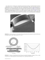
A promising on-chip test structure has been developed over the years by Senturia and his students; it is
shown schematically in Figure 3.6.A voltage is applied between the conductive polysilicon beam and the sub-
strate to pull the beam down, and the voltage that causes the beam to make contact is a measure of its stiff-
ness. This concept was introduced early on by Petersen and Guarnieri (1979) and further developed by Gupta
et al. (1996). A similar approach and analysis were described by Zou et al. (1995). The considerable advantage
here is that the measurements can be made entirely with electrical probing in a manner similar to that used
to check microelectronic circuits. This opens the opportunity for process monitoring and quality control.
The fixed ends clearly exert a major influence on the stiffness of the test structure. Kobrinsky et al.
(1999) have thoroughly examined this effect and shown its importance. The problem is that a particular
manufacturing process, or even variations within the same process, may etch the substrate slightly
differently and change the rigidity of the ends. Nevertheless, this is a potentially very useful method for
monitoring the consistency of MEMS materials and processes.
Zhang et al. (2000) recently conducted a thorough study of silicon nitride in which microbridges
(fixed–fixed beams) were deflected using a nanoindenter with a wedge-shaped indenter. By fitting the meas-
ured force-deflection records to their analytical model,they extracted both Young’s modulus and residual stress.
3.3.6.3 In-Plane Bending
In-plane bending may be a more appropriate test method in that the structural supports of MEMS accelerom-
eters are subjected to that mode of deformation. Jaecklin et al. (1994) pushed long, thin cantilever beams
with a probe until they broke; optical micrographs gave the maximum deflections, from which the fracture
3-10 MEMS: Introduction and Fundamentals
(a)
(b)
y
x
H
L
FIGURE 3.6 Schematic of a fixed-fixed beam. (Reprinted with permission from Kobrinsky, M. et al. [1999]
“Influence of Support Compliance and Residual Stress on the Shape of Doubly-Supported Surface Micromachined
Beams,” MEMS Microelectromechanical Systems 1, pp. 3–10, ASME, New York.)
© 2006 by Taylor & Francis Group, LLC
strain was determined. Jones et al. (1996) constructed a test structure consisting of cantilever beams of
different lengths fastened to a movable shuttle. As the shuttle was pushed, the beams contacted fixed stops
on the substrate; the deformed shape was videotaped and the fracture strain determined. Figure 3.7 is a
photograph of one of their deformed specimens.
Kahn et al. (1996) developed a double cantilever beam arrangement to measure the fracture toughness
of polysilicon and used the measured displacement between the two beams to determine Young’s modu-
lus via a finite element model. The beams were separated by forcing a mechanical probe between them
and pushing it toward the notched end. Fitzgerald et al. (1998) have taken a similar approach to measure
crack growth and fracture toughness in single-crystal silicon, but they use a clever structure that permits
opening the beams by compression of cantilever extensions.
3.3.6.4 Bending of Larger Specimens
Microelectromechanical technology is not restricted to thin-film structures, although they are far-and-
away predominant. Materials fabricated with thicknesses on the order of tens or hundreds of microns are
of current interest and likely to become more important in the future.
Ruther et al. (1995) manufactured a microtesting system using the LIGA process to test electroplated
copper. The interesting feature is that the in-plane cantilever beam and the test system are fabricated
together on the die; however, this requires a rather complex assembly. Stephens et al. (1998) fabricated rows
of LIGA nickel beams sticking up from the substrate and then measured the force applied near the upper
tip of the beam while displacing the substrate. The resulting force-displacement curve permitted extraction
of Young’s modulus, and the recorded maximum force gave a modulus of rupture.
Mechanical Properties of MEMS Materials 3-11
FIGURE 3.7 A polysilicon cantilever beam subjected to in-plane bending. The beam is 2.8 mm wide, and the verti-
cal distance between the fixed end at the bottom and the deflected end at the top is 70 mm. (Reprinted with permis-
sion from Sharpe, W.N., Jr., et al. [1998] “Round-Robin Tests of Modulus and Strength of Polysilicon,”
Microelectromechanical Structures for Materials Research Symposium, pp. 56–65.)
© 2006 by Taylor & Francis Group, LLC
Larger structures, such as the microengine under development at the Massachusetts Institute of
Technology, have thicknesses on the order of several millimeters. It then becomes necessary to test specimens
of similar sizes in what is sometimes called the mesocale region, whose dimensions generally range from
0.1 mm to 1 cm. Single-crystal silicon is the material of interest for initial versions, and Chen et al. (1998)
have developed a method for bend testing square plates simply supported over a circular hole and record-
ing the force as a small steel ball is pushed into the center of the plate. Fracture strengths are obtained,
and this efficient arrangement permits study of the effects of various manufacturing processes on the
load-carrying capability of the material.
3.3.7 Resonant Structure Tests
Frequency and changes in frequency can be measured precisely, and elastic properties of modeled struc-
tures can be determined. The microstructures can be very small and excited by capacitive comb-drives,
which require only electrical contact. This makes this approach suitable for on-chip testing; in fact, the
MUMPs process at Cronos includes a resonant structure on each die. That microstructure moves paral-
lel to the substrate, but others vibrate perpendicularly.
Petersen and Guarnieri (1979) introduced the resonant structure concept in 1979 by fabricating arrays of
thin, narrow cantilever beams of various lengths extending over an anisotropically etched pit in the substrate.
The die containing the beams was excited by variable frequency electrostatic attraction between the substrate
and the beams, and the vibration perpendicular to the substrate was measured by reflection from an incident
laser beam, as shown by the schematic in Figure 3.8. Yang and Fujita (1997) used a similar approach to study
the effect of resistive heating on U-shaped beams. Commercial AFM cantilevers were tested in a similar man-
ner by Hoummady et al. (1997), who measured the higher resonant modes of a cantilever beam with a mass
on the end. Zhang et al. (1991) measured vibrations of a beam fixed at both ends by using laser interferom-
etry. Michalicek et al. (1995) developed an elaborate and carefully modeled micromirror that was excited by
electrostatic attraction. Deflection was also measured by laser interferometry, and experiments determined
Young’s modulus over a range of temperatures as well as validating the model.
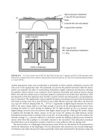
Microstructures that vibrate parallel to the plane of the substrate require less processing because the
substrate does not have to be removed. Biebl et al. (1995b) introduced this concept, and Kahn et al. (1998)
have used a more recent version to study the effects of heating on the Young’s modulus of films sputtered
3-12 MEMS: Introduction and Fundamentals
CW
He Ne
laser
Detector
Silicon substrate
Variable
frequency
oscillator
FIGURE 3.8 Schematic of the resonant structure system of Petersen and Guarnieri (1979). (Reprinted with per-
mission from Petersen, K.E., and Guarnieri, C.R. [1979] “Young’s Modulus Measurements of Thin Films Using
Micromechanics,” J. Appl. Phys. 50, pp. 6761–66.)
© 2006 by Taylor & Francis Group, LLC
onto the structure. Figure 3.9 is a SEM image of their structure, which is easy to model. Pads A, B, C,
and D are fixed to the substrate; the rest of the structure is free. Electrostatic comb-drives excite the
two symmetrical substructures, which consist of four flexural springs and a rigid mass. The resonant
frequency of this device is around 47 kHz. Brown et al. (1997) have developed a different approach
in which a small notched specimen is fabricated as part of a large resonant fan-shaped component. This
resonant structure, shown in Figure 3.10, has been used primarily for fatigue and crack growth studies,
Mechanical Properties of MEMS Materials 3-13
120 µm
FIGURE 3.9 Scanning electron micrograph of the in-plane resonant structure of Kahn et al. (1998). (Reprinted with
permission from Kahn, H. et al. [1998] “Heating Effects on the Young’s Modulus of Films Sputtered onto
Micromachined Resonators,” Microelectromechanical Structures for Materials Research Symposium, pp. 33–38.)
120 µm
FIGURE 3.10 Scanning electron micrograph of the in-plane resonant structure of Brown et al. (1997). (Reprinted
with permission from Brown, S.B. et al. [1997] “Materials Reliability in MEMS Devices,” Proc. Int. Solid-State Sensors
and Actuators Conf. — Transducers ’97, pp. 591–93. © 1997 IEEE.)
© 2006 by Taylor & Francis Group, LLC
but Young’s modulus of polysilicon has been extracted from its finite element model [Sharpe
et al., 1998c].
3.3.8 Membrane Tests
It is relatively easy to fabricate a thin membrane of test material by etching away the substrate; the mem-
brane is then pressurized and the measured deflection can be used to determine the biaxial modulus. An
advantage of this approach is that tensile residual stress in the membrane can be measured, but the value
of Poisson’s ratio must be assumed. This method, often called bulge testing, was first introduced by Beams
(1959), who tested thin films of gold and silver and measured the center deflection of the circular mem-
brane as a function of applied pressure. Jacodine and Schlegel (1966) used this approach to measure
Young’s modulus of silicon oxide. Tabata et al. (1989) tested rectangular membranes whose deflections
were measured by observations of Newton’s rings, as did Maier-Schneider et al. (1995). The variation of
Hong et al. (1990) used circular membranes with force deflection measured at the center with a nanoin-
denter. Pressurized square membranes with the deflection measured by a stage-mounted microscope
were tested by Walker et al. (1990) to study the effect of hydrofluoric acid exposure on polysilicon; a sim-
ilar approach to determine biaxial modulus, residual stress, and strength was used by Cardinale and
Tustison (1992). Vlassak and Nix (1992) eliminated the need to assume a value of Poisson’s ratio by test-
ing rectangular silicon nitride films with different aspect ratios. More recently, Jayaraman et al. (1998)
used this same approach to measure Young’s modulus and Poisson’s ratio of polysilicon.
3.3.9 Indentation Tests
A nanoindenter is, in the fewest words, simply a miniature and highly sensitive hardness tester. It measures
both force and displacement, and modulus and strength can be obtained from the resulting plot. Penetration
depths can be very small (a few nanometers), and automated machines permit multiple measurements to
enhance confidence in the results and also to scan small areas for variations in properties.
Weihs et al. (1989) measured the Young’s modulus of an amorphous silicon oxide film and a nontex-
tured gold film with a nanoindenter and obtained only limited agreement with their microbeam deflec-
tion experiments. The modulus measured by indentation was consistently higher, and the large pressure
of the indenter tip was the probable cause. Taylor (1991) used nanoindenter measurements restricted to
penetrations of 200 nm into silicon nitride films 1 µm thick to study the effects of processing on mechan-
ical properties. Young’s modulus decreased with decreasing density of the films.
Bhushan and Li (1997) have studied the tribological properties of MEMS materials, and Li and Bhusan
(1999) used a nanoindenter to measure the modulus and a microhardness tester to measure the fracture
toughness of thin films. Measurements of Young’s modulus of polysilicon showed a wide scatter. Bucheit
et al. (1999) examined the mechanical properties of LIGA-fabricated nickel and copper by using a
nanoindenter as one of the tools. In most cases, Young’s modulus from nanoindenter measurements were
higher than from tension tests, but the nanoindenter does allow looking at both sides of the thin film as
well as at sectioned areas.
3.3.10 Other Test Methods
The readily observed buckling of a column-like structure under compression can be used to measure
forces in specimens; if the specimen breaks, the fracture strength can be estimated. Tai and Muller (1988)
fabricated long, thin polysilicon specimens with one end fixed and the other enclosed in slides. The mov-
able end was pushed with a micromanipulator, and its displacement when the structure buckled was used
to determine the strain (not stress) at fracture. Ziebart and colleagues have analyzed thin films with var-
ious boundary conditions ranging from fixed along two sides [Ziebart et al., 1997] to fixed on all four
sides [Ziebart et al., 1999]. The first arrangement permitted the measurement of Poisson’s ratio when the
side supports were compressed, and the second determined prestrains induced by processing. Beautiful
patterns are obtained, but the analysis and the specimen preparation can be time consuming.
3-14 MEMS: Introduction and Fundamentals
© 2006 by Taylor & Francis Group, LLC
Another clever approach based on buckling is described by Cho et al. (1997). They etched away the silicon
substrate under an overhanging strip of diamond-like carbon film and used the buckled pattern to deter-
mine the residual stress in the film. A more traditional creep test was used by Teh et al. (1999) to study
creep in 2 ϫ 2ϫ 100 µm polysilicon strips fixed at each end. As current passed through the specimens,
they heated up, and their buckled deflection over time at a constant current was used to extract a strain-
vs time creep curve. This approach is complicated by the nonuniformity of the strain in the specimen.
Although torsion is an important mode of deformation in certain MEMS, such as digital mirrors, few
test methods have been developed. Saif and MacDonald (1996) introduced a system to twist very small
(10 µm long and 1 µm on a side) pillars of single-crystal silicon and measure both the force and deflec-
tion. Larger (300 µm long with side dimensions varying from 30 to 180 µm) of both silicon and LIGA
nickel were tested by Schiltges et al. (1998). Emphasis was on the elastic properties only with the shear
modulus values agreeing with expected bulk values.
Nondestructive measurements of elastic properties of thin films can be accomplished with laser-
induced ultrasonic surface waves. A laser pulse generates an impulse in the film, and a piezoelectric trans-
ducer senses the surface wave. In principle, Young’s modulus, density, and thickness can be determined,
but this cannot be achieved for all combinations of film and substrate materials. Schneider and Tucker
(1996) describe this test method and present results for a wide range of films; the Young’s modulus
values generally agree with other thin-film measurements. A drawback here is the planar size of the film;
the input and output must be several millimeters apart. A related technique uses Brillouin scattering
as described in Monteiro et al. (1996).
3.3.11 Fracture Tests
Single-crystal silicon and polysilicon are both brittle materials, and it is therefore natural to want to
measure their fracture toughness. This is even more difficult than measuring their fracture strength
because of the need for a crack with a tip radius that is small relative to the specimen dimensions.
Photolithography processes for typical thin films have a minimum feature radius of approximately
1 mm. Fan et al. (1990), Sharpe et al. (1997f) and Tsuchiya et al. (1998) have tested polysilicon films in
tension using edge cracks, center cracks, and edge cracks, respectively. Kahn et al. (1999) modeled a
double-cantilever specimen with a long crack and wedged it open with an electrostatic actuator.
Fitzgerald et al. (1999) prepared sharp cracks in double-cantilever silicon crystal specimens by etch-
ing, and Suwito et al. (1997) modeled the sharp corner of a tensile specimen to measure the fracture
toughness. Van Arsdell and Brown (1999) introduced cracks at notches in polysilicon with a diamond
indenter. A promising new approach using a focused ion beam (FIB) can prepare cracks with tip radii of
30 nm according to K. Jackson (pers. comm.).
3.3.12 Fatigue Tests
Many MEMS operate for billions of cycles, but that kind of testing is conducted on microdevices, such as
digital mirrors instead of the more basic reversed bending or push–pull tests so familiar to the metal
fatigue community. Brown and his colleagues have developed a fan-shaped, electrostatically driven
notched specimen that has been used for fatigue and crack growth studies [Brown et al., 1993, 1997; Van
Arsdell and Brown, 1999]. Minoshima et al. (1999) have tested single-crystal silicon in bending fatigue,
and Sharpe et al. (1999) reported some preliminary tension–tension tests on polysilicon. As noted earlier,
fatigue data are reported as stress-vs life plots, and Kapels et al. (2000) present a plot that looks much
like one would expect for a metal; the allowable applied stress decreases from 2.9 GPa for a monotonic
test to 2.2 GPa at one million cycles.
3.3.13 Creep Tests
Some MEMS are thermally actuated, so the possibility of creep failure exists. No techniques similar to the
familiar dead-weight loading to produce strain-vs time curves exist. Teh et al. (1999) have observed the
buckling of heated fixed-end polysilicon strips.
Mechanical Properties of MEMS Materials 3-15
© 2006 by Taylor & Francis Group, LLC
3.3.14 Round-Robin Tests
Mechanical testing of MEMS materials presents unique challenges as the above review shows.
Convergence of test methods into a standard is still far in the future, but progress in that direction usu-
ally begins with a round-robin program in which a common material is tested by the method-of-choice
in participating laboratories. That first step was taken in 1997/1998 with the results reported at the Spring
1998 meeting of the Materials Research Society [Sharpe et al., 1998c]. Polysilicon from the MUMPs 19
and 21 runs of Cronos were tested in bending (Figure 3.7), resonance (Figure 3.10), and tension (Figure
3.3). Young’s modulus was measured as 174 Ϯ 20GPa in bending, 137 Ϯ 5GPa in resonance, and
139 Ϯ 20 GPa in tension. Strengths in bending were 2.8 Ϯ 0.5GPa, in resonance 2.7 Ϯ 0.2 GPa, and in
tension 1.3 Ϯ 0.2 GPa. These variations were alarming but in retrospect perhaps not too surprising given
the newness of the test methods at that time.
A more recent interlaboratory study of the fracture strength of polysilicon manufactured at Sandia has
been arranged by LaVan et al. (2000b).Strengths measured on similar tensile specimens by Tsuchiya in Japan
and at Johns Hopkins were 3.23 Ϯ 0.25 and 2.85 Ϯ 0.40GPa respectively. LaVan tested in tension with a dif-
ferent approach and obtained 4.27 Ϯ 0.61 GPa. It seems clear that more effort needs to be devoted to the
development of test methods that can be used in a standardized manner by anyone who is interested.
3.4 Mechanical Properties
This section lists in tabular form the results of measurements of mechanical properties of materials used
in MEMS structural components. Its intent is not only to provide values of mechanical properties but also
to supply references on materials and test methods of interest. Because as yet no standard test method
exists and such a wide variety in the values is obtained for supposedly identical materials, readers with a
strong interest in the mechanical behavior of a particular material can use the tables to identify pertinent
references.
Almost all the data listed comes from experiments directly related to free-standing structural films. The
only exceptions are the results from ultrasonic measurements by Schneider and Tucker (1996) because
they tested a number of materials of interest. Including information on the processing conditions for each
reference proved too cumbersome, but the short comments in the tables should be useful. Many of the
results are average values of multiple replications, and the standard deviations are included when they are
available. Most of the materials used in MEMS are ceramics and show linear and brittle behavior, in
which case only the fracture strength is listed. The tables for ductile materials show both yield and ulti-
mate strengths. Also note that the values in the tables are edited from a larger list. Some of the same val-
ues have been presented in two different venues (e.g., aconference publication and a journal paper), in
which case the more archival version was referenced. A limited number of studies have been conducted
on the effects of environment (temperature, hydrofluoric acid, saltwater, etc.) on MEMS materials, but
that area of research is in its infancy and is not included.
First, typical stress–strain curves are plotted in Figure 3.11 to compare the mechanical behavior
of MEMS materials with a common structural steel, A533-B, which is moderately strong (yield strength
of 440 MPa) but ductile and tough. Polysilicon is linear and brittle and much stronger. LIGA nickel is
ductile and considerably stronger than bulk pure nickel. One must test materials as they are produced
for MEMS instead of relying on bulk material values.
The microstructure of these MEMS materials is also different from that of bulk materials. The physics of
the thin-film deposition process cause the grains to be columnar in a direction perpendicular to the film as
shown in Figure 3.12. The result is similar to the cross-section of a piece of bamboo or wood, and the mate-
rial is transversely isotropic. Test methods are not sensitive enough to measure the anisotropic constants.
Table 3.1 lists metal films tested in a free-standing manner such as would be appropriate for use in
MEMS. Only aluminum is currently used in that fashion, but the other materials are commonly used in
the electronics industry and may be of interest. Note that all of the materials are ductile; the complete
stress–strain curves are included in many of the references. The values of Young’s modulus as measured
for pure bulk materials are listed for reference.
3-16 MEMS: Introduction and Fundamentals
© 2006 by Taylor & Francis Group, LLC
Mechanical Properties of MEMS Materials 3-17
0
0.2
0.4
0.6
0.8
1
1.2
1.4
–0.5 0.50 1.51
2
Strain (%)
Stress (GPa)
Polysilicon
Polysilicon
Steel
Nickel
FIGURE 3.11 Representative stress–strain curves of polysilicon, electroplated nickel, and A-533B steel. These are
from microspecimens tested in the author’s laboratory.
20 µm
(a)
(
b
)
FIGURE 3.12 Microstructure of two common MEMS materials. Note the columnar grain structure perpendicular to the
plane of the film. (a) Polysilicon deposited in two layers; the bottom layer is 2.0µm thick and the top one is 1.5µm thick.
(Reprinted with permission from Sharpe et al. [1998c] “Round-Robin Tests of Modulus and Strength of Polysilicon,” in
Microelectromechanical Structures for Materials Research, Materials Research Society Symposium 518, pp. 56–65, 15–16
April, Francisco. © 1998 IEEE.) (b) Nickel electroplated into LIGA molds. (Reprinted with permission from Sharpe et al.
[1997d] “Measurements of Young’s Modulus, Poisson’s Ratio,and Tensile Strength of Polysilicon,” Proc. IEEE Tenth Annual
Int. Workshop on Micro Electro Mechanical Systems, pp. 424–29, 26–30 January, Nagoya, Japan. © 1998 IEEE.)
© 2006 by Taylor & Francis Group, LLC
Carbon can be deposited to form an amorphous or crystalline structure that is often referred to as
diamond-like carbon, (DLC). Diamond itself has a very high stiffness and strength as well as a low coef-
ficient of friction; for these reasons DLC offers exciting possibilities in MEMS. The very limited results to
date, shown in Table 3.2, support this line of reasoning although they are far too sparse to be conclusive.
Electroplated nickel and nickel–iron MEMS, usually manufactured via the LIGA process, offer the pos-
sibility of larger and stronger actuators and connectors. The microstructure and mechanical properties of
an electroplated material are highly dependent upon the composition of the plating bath and on the
current and temperature. Similarly, the composition of a nickel–iron alloy significantly affects its charac-
teristics. Young’s modulus and strength values are listed in Tables 3.3 and 3.4 for nickel and nickel–iron
respectively. The modulus of bulk nickel is around 200 GPa, and the yield strength of pure fine-grained
nickel is approximately 60 MPa [ASM, 1990]. Table 3.3 shows that the modulus of nickel is generally
somewhat lower and the strength considerably higher. Nickel–iron has a smaller modulus, as expected,
but can be a very strong material as seen from the limited results in Table 3.4.
3-18 MEMS: Introduction and Fundamentals
TABLE 3.1 Metals
Young’s Yield Ultimate
Modulus Strength Strength
Metals (GPa) (GPa) (GPa) Method Comments Ref.
Aluminum 8–38 — 0.04–0.31 Te nsion 110–160 µm thick Hoffman (1989)
modulus of bulk 40 — 0.15 Te nsion 1.0 µm thick Ogawa et al. (1996)
material ϭ 69 GPa
69–85 —— Bending Var ious lengths Comella and
Scanlon (2000)
Copper 86–137 0.12–0.24 0.33–0.38 Tension Plated; annealed Buchheit et al.
(1999)
modulus of bulk 108–145 —— Indentation Var ious locations Buchheit et al.
material ϭ 117 GPa (1999)
98 Ϯ 4— — Tension Laser speckle Anwander et al.
(2000)
Gold 40–80 — 0.2–0.4 Te nsion 0.06–16 µm thick Neugebauer (1960)
modulus of bulk 57 0.26 —Bending ϳ1 µm thick Weihs et al. (1988)
material ϭ 74 GPa
74 —— Indentation ϳ1 µm thick Weihs et al. (1988)
82 — 0.33–0.36 Tension 0.8 µm thick Emery et al. (1997)
—— 0.22–0.27 Bending Composite beam Kraft et al. (1998)
Titanium
modulus of bulk 96 Ϯ 12 — 0.95 Ϯ 0.15 Te nsion 0.5µm thick Ogawa et al. (1997)
material ϭ 110 GPa
Ti–Al–Ti — 0.07–0.12 0.14–0.19 Tension Composite film Read and Dally
(1992)
TABLE 3.2 Diamond-Like Carbon
Young’s Fracture
Modulus (GPa) Strength (GPa) Method Comments Ref.
600–1100 0.8–1.8 Bending Hot flame deposited Hollman et al. (1995)
800–1140 — Ultrasonic CVD diamond Schneider and Tucker (1996)
150–800 — Ultrasonic Laser arc deposited Schneider and Tucker (1996)
580 — Brillouin CVD diamond Monteiro et al. (1996)
94–128 — Buckling Poisson’s ratio ϭ 0.22 Cho et al. (1998)
— 8.5 Ϯ 1.4 Tension Amorphous diamond LaVan et al. (2000a)
© 2006 by Taylor & Francis Group, LLC
The most common MEMS material, polysilicon, is also the most tested, as Table 3.5 demonstrates. The
stiffness coefficients of single-crystal silicon are well established, and the modulus in different directions
can vary from 125 to 180 GPa [Sato et al., 1997]. Aggregate theories predict that randomly oriented poly-
crystalline silicon should have a Young’s modulus between 163 and 166 GPa [Guo et al., 1992; Jayaraman
et al., 1999]. Most of the modulus values in Table 3.5 are near or within this range, but some vary widely,
especially when a test method is first used. An estimate of what the fracture strength should be is more
difficult as it depends on the flaws in the material. Even though strength is easier to measure than mod-
ulus (one needs to measure only force), there are fewer entries. This is because many of the bending, res-
onance, and bulge tests do not lead to failure in the specimen.
Single-crystal silicon has also been studied extensively, as Table 3.6 shows. The modulus values are
measured along particular crystallographic directions, so they should not be expected to compare with
the polysilicon values.
Silicon carbide holds promise for MEMS because of its expected high stiffness, strength, and chemical
and temperature stability; and Sarro (2000) provides a thorough overview of its potential. Bulk silicon
carbide is commonly available, but manufacturing processes for thin, free-standing films are still in devel-
opment. Table 3.7 lists results from the few tests to date; note that no strength values appear.
Mechanical Properties of MEMS Materials 3-19
TABLE 3.3 Nickel
Young’s Yield Ultimate
Modulus Strength Strength
(GPa) (GPa) (GPa) Method Comments Ref.
202 0.40 0.78 Te nsion Vibration for modulus Mazza et al. (1996b)
ϳ200 —— Ultrasonic 3–75 µm thick Schneider and Tucker (1996)
168–182 0.1 Ϯ 0.01 — FE Model Microgrippers Basrour et al. (1997)
205 —— Resonance Also fatigue Dual et al. (1997)
68* —— Torsion *Shear modulus Dual et al. (1997)
176 Ϯ 30 0.32 Ϯ 0.03 0.55 Te nsion ϳ200 µm thick Sharpe et al. (1997e)
131–160 0.28–0.44 0.46–0.76 Te nsion Var ied current Christenson et al. (1998)
231 Ϯ 12 1.55 Ϯ 05 2.47 Ϯ 0.07 Te nsion 6 µm thick Greek and Ericson (1998)
180 Ϯ 12 —— Resonance Film on resonator Kahn et al. (1998)
181 Ϯ 36 0.33 Ϯ 0.03 0.44 Ϯ 0.04 Te nsion LIGA 3 films Sharpe and McAleavey (1998)
158 Ϯ 22 0.32 Ϯ 0.02 0.52 Ϯ 0.02 Te nsion LIGA 4 films Sharpe and McAleavey (1998)
182 Ϯ 22 0.42 Ϯ 0.02 0.60 Ϯ 0.01 Te nsion HI-MEMS films Sharpe and McAleavey (1998)
153 Ϯ 14 — 1.28 Ϯ 0.24* Bending *Modulus of rupture Stephens et al. (1998)
156 Ϯ 9 0.44 Ϯ 0.03 —Tension Current ϭ 20 ma/cm
2
Buchheit et al. (1999)
92 0.06/0.16* —*Tension/ Annealed Buchheit et al. (1999)
compression
160 Ϯ 1 0.28/0.27* —*Tension/ Current ϭ 50 ma/cm
2
Buchheit et al. (1999)
compression
146–184 — — Indentation Various locations Buchheit et al. (1999)
194 — — Tension Laser speckle Anwander et al. (2000)
TABLE 3.4 Nickel–Iron
Young’s Yield Ultimate
Modulus Strength Strength
(GPa) (GPa) (GPa) Method Comments Ref.
65 — — Fixed ends 80% Ni–20% Fe Chung and Allen (1996)
119 0.73 1.62 Tension 50% Ni–50% Fe Dual et al. (1997)
115 — — Resonance 50% Ni–50% Fe Dual et al. (1997)
15–54* — — Torsion *Shear modulus Dual et al. (1997)
155 — 2.26 Tension Electroplated Greek and Ericson (1998)
— 1.83–2.20 2.26–2.49 Tension HI-MEMS films Sharpe and McAleavey (1998)
© 2006 by Taylor & Francis Group, LLC
Silicon nitride commonly appears in both MEMS and in microelectronics as an insulating layer, and
interest in its use as a structural material is growing. Table 3.8 lists its properties. Silicon oxide is also typ-
ically included in a MEMS or microelectronics process, but it is less likely to be used as a structural com-
ponent because of its low stiffness and strength, as shown in Table 3.9.
To date, the main application of the polymer SU-8 is as a mask material for thicker electroplated metal
MEMS. Its use as a structural component is possible, but the values of stiffness and strength in Table 3.10
are very low.
Fracture toughness values have been measured for polysilicon; Table 3.11 lists the results. Note that this
is not the plane-strain fracture toughness that is a materials property; care is needed, as some authors list
this value as KIc.
3-20 MEMS: Introduction and Fundamentals
TABLE 3.5 Polysilicon
Young’s Fracture
Modulus (GPa) Strength (GPa) Method Comments Ref.
160 — Bulge Obtains residual stress Tabata et al. (1989)
123 — Fixed ends Heavily doped Tai and Muller (1990)
190–240 — Bulge Various etches Walker et al. (1990)
164–176 2.86–3.37 Tension Varied grain size Koskinen et al. (1993)
— 2.11–2.77 Bending CMOS process Biebl et al. (1995a)
147 Ϯ 6 — Resonance Temperature effects Biebl et al. (1995b)
170 — Bending Varied doping Biebl and Philipsborn (1995)
— 0.57-0.77 Tension Weibull analysis Greek et al. (1995)
151–162 — Bulge Various anneals Maier-Schneider et al. (1995)
163 — Resonance Temperature effects Michalicek et al. (1995)
171–176 — Fixed ends Pull-in voltage Zou et al. (1995)
149 Ϯ 10 — Fixed ends Pull-in voltage Gupta et al. (1996)
150 Ϯ 30 — Resonance 10 µm thick Kahn et al. (1996)
140* 0.70 Tension *Approximate Read and Marshall (1996)
152–171 — Ultrasonic 0.4 µm thick Schneider and Tucker (1996)
176–201 — Indentation Different depths Bhushan and Li (1997)
160–167 1.08–1.25 Tension Weibull analysis Greek and Johansson (1997)
178 Ϯ 3 — Fixed ends Ph.D. thesis Gupta (1997)
169 Ϯ 6 1.20 Ϯ 0.15 Tension Poisson’s ratio ϭ 0.22 Ϯ .01 Sharpe et al. (1997d)
174 Ϯ 20 2.8 Ϯ 0.5 Bending Tested by Jones et al. Sharpe et al. (1998c)
132 — Tension Tested by Chasiotis et al. Sharpe et al. (1998c)
137 Ϯ 5 2.7 Ϯ 0.2 Resonance Tested by Brown et al. Sharpe et al. (1998c)
140 Ϯ 14 1.3 Ϯ 0.1 Tension Tested by Sharpe et al. Sharpe et al. (1998c)
172 Ϯ 7 1.76 Tension 10 µm thick Greek and Ericson (1998)
162 Ϯ 4 — Bulge Poisson’s ratio ϭ 0.19 Ϯ .03 Jayaraman et al. (1998)
168 Ϯ 4 — Resonance 0.45–0.9 µm thick Kahn et al. (1998)
135 Ϯ 10 — Bending AFM Serre et al. (1998)
95–167 — Indentation Also wear tests Sundararajan and Bhushan
(1998)
167 2.0–2.7 Tension Modulus from bulge; P-doped Tsuchiya et al. (1998a)
163 2.0–2.8 Tension Modulus from bulge; Tsuchiya et al. (1998a)
undoped
— 1.8–3.7 Tension Different sizes and anneals Tsuchiya et al. (1998b)
95/175 — Indentation Doped and undoped Li and Bhushan (1998)
198 — Bending Capacitive device Que et al. (1999)
166 Ϯ 5 1.0 Ϯ 0.1 Tension Force-displacement Chasiotis and Knauss (2000)
— 4.27 Ϯ 0.61 Tension By LaVan et al. LaVan et al. (2000b)
— 2.85 Ϯ 0.40 Tension By Sharpe et al. LaVan et al. (2000b)
— 3.23 Ϯ 0.25 Tension By Tsuchiya et al. LaVan et al. (2000b)
158 Ϯ 8 1.56 Ϯ 0.25 Tension Size effects Sharpe and Jackson (2000)
159 and 169 — Tension Two specimens from Sharpe Yi (pers. comm.)
— 3.2 Ϯ 0.3 Bending Assumed E ϭ 160 GPa Jones et al. (2000)
— 2.9 Ϯ 0.5 Tension 4 µm thick Kapels et al. (2000)
— 3.4 Ϯ 0.5 Bending 4 µm thick Kapels et al. (2000)
© 2006 by Taylor & Francis Group, LLC
Poisson’s ratio is an important materials property when the stress state is biaxial, but only a very lim-
ited number of measurements have been made. Those are listed in the comments columns of the tables.
The question of the effect of size on the strength of MEMS materials often arises. This is because
MEMS structural components can be on the same size scale as fine single-crystal “whiskers” of materials,
which can have very high strengths, the premise being that they have fewer imperfections. However, there
are no dramatic increases in strength because the materials still have fine grains relative to the specimen
size. Tsuchiya et al. (1998) found an increase in the tensile strength of polysilicon specimens 2.0µm thick
as their length increased from 30 to 300 µm, but the gain was only 30%. Recent results show that the mod-
ulus of polysilicon does not vary with specimen size, but the strength increases from 1.21 to 1.65 GPa with
decreasing specimen size [Sharpe et al., 2001]. From a practical point of view, the effect of size on strength
for common MEMS structural components is not a concern.
On the other hand, Namazu et al. (2000) tested silicon crystal beams ranging in width from 0.2 to
1.04 mm, in thickness from 0.25 to 0.52 mm and in length from 6 to 9.85 mm. The beams were prepared
by anisotropic etching; the smallest were tested using an atomic force microscope, and the largest with a
Mechanical Properties of MEMS Materials 3-21
TABLE 3.6 Silicon Crystals
Young’s Modulus (GPa) Fracture Strength (GPa) Method Comments Ref.
177 Ϯ 18 2.0–4.3 Bending ͗110͘ Johansson et al. (1988)
188 — Indentation Weihs et al. (1989)
163 Ͼ3.4 Bending ͗110͘ Weihs et al. (1989)
122 Ϯ 2 — Bending ͗110͘ Ding et al. (1989)
125 Ϯ 1 — Resonance ͗110͘ Ding et al. (1989)
131 — Resonance Zhang et al. (1991)
173 Ϯ 13 — Bending ͗110͘ Osterberg et al. (1994)
147 0.26–0.82 Tension ͗110͘ Cunningham et al. (1995)
— 8.5–20 Torsion Shear and normal Saif and MacDonald (1996)
60–200 — Indentation Various doping Bhushan and Li (1997)
130 — Resonance ͗100͘ Dual et al. (1997)
75 — Torsion Shear modulus Dual et al. (1997)
125–180 1.3–2.1 Tension Three orientations Sato et al. (1997)
— 9.5–26.4 Bending Various etches Chen et al. (1998)
— 0.7–3.0 Bending Measured roughness Chen et al. (1999)
142 Ϯ 9 1.73 Tension ͗100͘ Greek and Ericson (1998)
165 Ϯ 20 2–8 Bending Fatigue tests also Komai et al. (1998)
168 — Indentation ͗100͘ Li and Bhushan (1999)
— 0.59 Ϯ 0.02 Tension ͗100͘ Mazza and Dual (1999)
— 2–6 Bending Fatigue also Minoshima et al. (1999)
169.2 Ϯ 3.5 0.6–1.2 Tension Various etches Yi and Kim (1999b)
115–191 — Tension Three orientations Yi and Kim (1999c)
164.9 Ϯ 4 — Tension Laser speckle Anwander et al. (2000)
169.9 0.5–17 Bending Various sizes Namazu et al. (2000)
TABLE 3.7 Silicon Carbide
Young’s Fracture
Modulus (GPa) Strength (GPa) Method Comments Ref.
394 — Bulge 3C–SiC Tong and Mehregany (1992)
88 Ϯ 10 to — Bulge + indentation Amorphous SiC El Khakani et al. (1993)
242 Ϯ 30
694 — Resonance 3C–SiC Su and Wettig (1995)
100–150 — Ultrasonic 0.2–0.3 µm thick Schneider and Tucker (1996)
331 — Bulge 3C–SiC; assumed Mehregany et al. (1997)
n ϭ 0.25 196 — Acoustic microscopy Amorphous SiC Cros et al. (1997)
and 273
395 — Indentation 3C–SiC Sundararajan and Bhushan (1998)
470 Ϯ 10 — Bending 3C–SiC Serre et al. (1999)
© 2006 by Taylor & Francis Group, LLC
microhardness tester. The mean bending strengths covered an astonishing range from 0.47 to 17.5 GPa —
a factor of 37.
3.5 Initial Design Values
If the manufacturing and testing technology for materials used in MEMS were as fully developed as those
associated with common structural materials, such as aluminum, for example, then this entire chapter
3-22 MEMS: Introduction and Fundamentals
TABLE 3.8 Silicon Nitride
Young’s Fracture
Modulus (GPa) Strength (GPa) Method Comments Ref.
130–146 Ϯ 20% — Resonance ϳ0.3 µm thick Petersen and Guarnieri (1979)
230 and 330 — Bulge Different processing Hong et al. (1990)
373 — Fixed ends Low stress Tai and Muller (1990)
101–251* — Indentation *Assume Poisson’s ratio ϭ 0.27 Taylor (1991)
110 and 160* 0.39–0.42 Bulge *Biaxial modulus Cardinale and Tustison (1991)
222 Ϯ 3 — Bulge Poisson’s ratio ϭ 0.28 Ϯ 0.05 Vlassak and Nix (1992)
216 Ϯ 10 — Indentation Vlassak and Nix (1992)
230–265 — Ultrasonic 0.2–0.3 µm thick Schneider and Tucker (1996)
192 — Resonance Buchaillot et al. (1997)
194.25 Ϯ 1% — Resonance Hoummady et al. (1997)
130 — Buckling Ziebart et al. (1999)
290 7.0 Ϯ 0.9 Bending Kuhn et al. (2000)
202.57 Ϯ 15.80 12.26 Ϯ 1.69* Fixed ends *Bending strength Zhang et al. (2000)
255 Ϯ 3 6.4 Ϯ 1.1 Tension Poisson’s ratio ϭ 0.23 Ϯ 0.01 G. Coles (pers. comm.)
TABLE 3.9 Silicon Oxide
Young’s Modulus (GPa) Fracture Strength (GPa) Method Comments Ref.
66* — Bulge *Assumed n ϭ 0.18 Jaccodine and Schlegel (1966)
57–92 Ϯ 20% — Resonance Various depositions Petersen and Guarnieri (1979)
64 Ͼ0.6 Indentation Weihs et al. (1988)
83 — Bending Weihs et al. (1988)
— 0.6–1.9 Tension In vacuum and in air Tsushiya et al. (1999)
TABLE 3.10 SU-8
Young’s Yield Strength
modulus (GPa) (GPa) Ultimate Strength (GPa) Method Comments Ref.
ϳ3 — 0.12–0.13 Tension McAleavey et al. (1998)
1.5–3.1 0.03–0.05 0.05–0.08 Tension Strain by SIEM Chang et al. (2000)
TABLE 3.11 Fracture Toughness Values
Fracture Toughness
(MPa-m1/2) Test Method Material Ref.
1.8 Ϯ 0.3 Tension; edge crack Silicon nitride; two kinds Fan et al. (1990)
1.2 Indentation Silicon crystal DeBoer et al. (1993)
0.96–1.65 Double cantilever Silicon crystal Fitzgerald et al. (1999)
1.4 Ϯ 0.6 Tension; center crack Polysilicon Sharpe et al. (1997f)
1.9–4.5 Tension; edge crack Polysilicon Tsuchiya et al. (1997)
3.5–5.0 Notched specimen Polysilicon; various dopings Ballarini et al. (1998)
1.1–2.7 Notched specimen Polysilicon; various dopings Kahn et al. (1999)
1.2 Ϯ 0.3 Sharp precrack Polysilicon Kahn et al. (2000)
1.6 Ϯ 0.3 Tension; corner Polysilicon K. Jackson (pers. comm.)
1.0 Ϯ 0.1 Surface crack Polysilicon J. Bagdahn (pers. comm.)
© 2006 by Taylor & Francis Group, LLC
could have been reduced to a one-page table. However, that is not the case; the materials themselves are
new, and the test methods are still in their infancy. It may be useful to list “best guesses” at the material
properties of MEMS materials to be used in an initial design, and Table 3.12 does that. These are only esti-
mates, and the actual properties resulting from a particular manufacturing process may be quite differ-
ent from these nominal values.
Aluminum, copper, and gold have essentially the same modulus values as the bulk materials, but the
ultimate strengths are slightly higher than those found for commercially pure materials. Young’s modu-
lus for thin-film nickel can vary depending upon the deposition parameters, but it is conservative to
assume that it will be lower (at 180 GPa) than the 200 GPa expected for bulk pure nickel. There are fewer
results for nickel–iron, so the modulus of 120 GPa is only a rough estimate. However, it is clear that thin-
film nickel and nickel–iron alloys are quite a bit stronger than one would expect from knowledge of bulk
behavior.
The values listed for diamond-like carbon are only an optimistic guide. There are many variations of
this material, and very few test results. These properties are included because such a material would be
very attractive if it could be realized.
Polysilicon has certainly been thoroughly tested and is widely used, but there still is no “standard”value —
at least for Young’s modulus. The explanation for this is, of course, the difficulty in testing at this size scale,
but there is a clear trend toward a modulus in the neighborhood of 160GPa. An assumption of that num-
ber Ϯ10GPa can be used with confidence in the initial design of a microdevice. It is also clear that the
strength can vary depending upon the manufacturing process but will fall in the range of 1.2 to 3.0 GPa.
Single-crystal silicon has been thoroughly characterized to the point that it has been used as a
“standard material” to validate test systems. The modulus depends on orientation, and the strength range
is enormous with some extremely high values being reported.
Silicon carbide is widely promoted as a MEMS material, but conclusive measurements of its modulus
have yet to be made, and there are no measurements of strength. One should use the modulus value with
caution. The situation is better for silicon nitride, as it has been more widely used and tested.
Although Table 3.12 lists numbers to three significant figures, the reader will surely appreciate their
unreliability and wonder as to their value. But many other uncertainties occur between the initial design
and the product. Dimensions may not result as specified, and that can have a profound effect on the stiff-
nesses of small components. Boundary conditions may not be as specified either, due to variations in etch
release processes. Nevertheless, the values in Table 3.12 offer a starting point. Users should certainly refer
to the more detailed information in the other tables and probably should consult the appropriate references.
Acknowledgments
The author is grateful for the interactions with students and colleagues over the past five years that have
provided the background for this chapter. Vanessa Coleman’s assistance with preparation is appreciated.
Mechanical Properties of MEMS Materials 3-23
TABLE 3.12 Initial Design Values
Young’s Poisson’s Yield Ultimate or Fracture
Material Modulus (GPa) Ratio Strength (GPa) Strength (GPa)
Aluminum 70 — — 0.15
Copper 120 — 0.15 0.35
Gold 70 — — 0.30
Nickel 180 — 0.30 0.50
Nickel–iron 120 — 0.70 1.60
Diamond-like carbon 800 0.22 — 8.0
Polysilicon 160 0.22 — 1.2–3.0
Silicon crystal 125–180 — — Ͼ1.0
Silicon carbide 400 0.25 — —
Silicon nitride 250 0.23 — 6.0
Silicon oxide 70 — — 1.0
© 2006 by Taylor & Francis Group, LLC
The effort was sponsored by the Defense Advanced Research Projects Agency (DARPA) and Air Force
Research Laboratory, Air Force Materiel Command, USAF, under agreement number F30602-99-2-0553.
The U.S. government is authorized to reproduce and distribute reprints for governmental purposes
notwithstanding any copyright annotation thereon.
References
Amimoto, S.T., Chang, D.J., and Birkitt, A. (1998) “Stress Measurements in MEMS Using Raman
Spectroscopy,” Proc. SPIE 3512, pp. 123–29.
Anwander, M., Kaindl, G., Klein, M., and Weiss, B. (2000) “Noncontacting Laser Based Techniques for the
Determination of Elastic Constants of Thin Foils,” Micromat 2000, pp. 1100–3, 17–19 April, Berlin,
Germany.
ASM (1990) Metals Handbook, 10th ed., vol. 2, ASM International, Materials Park, OH, p. 1143.
ASTM (1970) Review of Developments in Plane Strain Fracture Toughness Testing, STP 463, American
Society for Testing and Materials, New York.
ASTM (2000a) Metals: Mechanical Testing; Elevated and Low-Temperature Tests; Metallography, vol. 03.01,
Annual Book of ASTM Standards, American Society for Testing and Materials, New York.
ASTM (2000b) Refractories: Carbon and Graphite Products; Activated Carbon, vol. 15.01, Annual Book of
ASTM Standards, American Society for Testing and Materials, New York.
Ballarini, R. (1998) “The Role of Mechanics in Microelectromechanical Systems (MEMS) Technology,”
AFRL-ML-WP-TR-1998-4209, Air Force Research Laboratory, Wright-Patterson Air Force Base, OH.
Ballarini, R., Mullen, R.L., Kahn, H., and Heuer, A.H. (1998) “The Fracture Toughness of Polysilicon
Microdevices,” in Microelectromechanical Structures for Materials Research, Materials Research
Society Symposium 518, pp. 137–42, 15–16 April, San Francisco.
Basrour, S., Robert, L., Ballandras, S., and Hauden, D. (1997) “Mechanical Characterization of
Microgrippers Realized by LIGA Technique,” in Proc. Int. Solid-State Sensors and Actuators Conf. —
Transducers ’97, pp. 599–602, 16–19 June, Chicago.
Beams, J.W. (1959) “Mechanical Properties of Thin Films of Gold and Silver,” in Proc. Int. Conf. Sponsored
by Air Force Office of Scientific Research, Air Research and Development Command and The General
Electric Research Laboratory ’59, pp. 183–92, 9–11 September, Bolton Landing, NY.
Benrakkad, M.S., Benitex, M.A., Esteve, J., Lopez-Villegas, J.M., Samitier, J., and Morante, J.R. (1995)
“Stress Measurement by Microraman Spectroscopy of Polycrystalline Silicon Structures,” J.
Micromech. Microeng. 5, pp. 132–35.
Bhushan, B., and Li, X. (1997) “Micromechanical and Tribological Characterization of Doped Single-
Crystal Silicon and Polysilicon Films for Microelectromechanical Systems Devices,” J. Mater. Res.
12, pp. 54–63.
Biebl, M., and von Philipsborn, H. (1995) “Fracture Strength of Doped and Undoped Polysilicon,”in Proc.
Int. Solid-State Sensors and Actuators Conf. — Transducers ’95, pp. 72–75, 25–29 June, Stockholm.
Biebl, M., Brandl, G., and Howe, R.T. (1995a) “Young’s Modulus of In-Situ Phosphorus-Doped Silicon,”
in Proc. Int. Solid-State Sensors and Actuators Conf. — Transducers ’95, pp. 80–83, 25–29 June,
Stockholm.
Biebl, M., Scheiter, T., Hierold, C., Philipsborn, H., and Klose, H. (1995b) “Micromechanics Compatible
with an 0.8 µm CMOS Process,” Sensor. Actuator. A (Phys.) 46–47, pp. 593–97.
Brown, S.B., Povirk, G., and Connally, J. (1993) “Measurement of Slow Crack Growth in Silicon and
Nickel Mechanical Devices,” in Proc. IEEE Micro Electro Mechanical Systems, pp. 99–104, 7–10
February, Fort Lauderdale.
Brown, S.B., Van Arsdell, W., and Muhlstein, C.L. (1997) “Materials Reliability in MEMS Devices,” in Proc.
Int. Solid-State Sensors and Actuators Conf. — Transducers ’97, pp. 591–93, 16–19 June, Chicago.
Buchaillot, L., Farnault, E., Hoummady, M., and Fujita, H. (1997) “Silcon Nitride Thin Films Young’s
Modulus Determination by an Optical Non Destructive Method,” Jpn. J. Appl. Phys., part 2 (Lett.)
36, pp. L794–L797.
3-24 MEMS: Introduction and Fundamentals
© 2006 by Taylor & Francis Group, LLC
Buchheit, T.E., Christenson, T.R., Schmale, D.T., and Lavan, D.A. (1999) “Understanding and Tailoring
the Mechanical Properties of LIGA Fabricated Materials,” in Materials Science of
Microelectromechanical Systems (MEMS) Devices, Materials Research Society Symposium 546, pp.
121–126, 1–2 December, Boston.
Cardinale, G.F., and Tustison, R.W. (1992) “Fracture Strength and Biaxial Modulus Measurement of
Plasma Silicon Nitride Films,” Thin Solid Films 207, pp. 126–30.
Chang, D.J., and Sharpe, W.N., Jr. (1999) “Mechanical Analysis and Properties of MEMS Materials,”
Microengineering for Aerospace Systems, The Aerospace Press of the Aerospace Corporation, El
Segundo, CA, pp. 73–118.
Chang, S., Warren, J., and Chiang, F.P. (2000) “Mechanical Testing of EPON SU-8 with SIEM,” in
Microscale Systems: Mechanics and Measurements Symposium,” Society for Experimental
Mechanics, pp. 46–49, 8 June, Orlando.
Chasiotis, I., and Knauss, W.G. (1998) “Mechanical Properties of Thin Polysilicon Films by Means of
Probe Microscopy,” Proc. SPIE 3512, pp. 66–75.
Chasiotis, I., and Knauss, W.G. (2000) “Instrumentation Requirements in Mechanical Testing of MEMS
Materials,” in Microscale Systems: Mechanics and Measurements Symposium, Society for
Experimental Mechanics, pp. 56–61, 8 June, Orlando.
Chen, K.S., Ayon, A., and Spearing, M. (1998) “Silicon Strength Testing for Mesoscale Structural
Applications,” in Microelectromechanical Structures for Materials Research, Materials Research
Society Symposium 518, pp. 123–30, 15–16 April, San Francisco.
Chen, K.S., Ayon, A., Lohner, K.A., Kepets, M.A., Melconian, T.K., and Spearing, S.M. (1999)
“Dependence of Silicon Fracture Strength and Surface Morphology on Deep Reactive Ion Etching
Parameters,” in Materials Science of Microelectromechanical Systems (MEMS) Devices, Materials
Research Society Symposium 546, pp. 21–26, 1–2 December, Boston.
Cho, S.J., Lee, K.R., Eun, K.Y., Han, J.H., and Ko, D.H. (1997) “A Method for Independent Measurement of
Elastic Modulus and Poisson’s Ratio of Diamond-Like Carbon Films,” in Thin-Films-Stresses and
Mechanical Properties VII, Materials Research Society Symposium 505, pp. 33–38, 1–5 December, Boston.
Cho, S.J., Kwang-Ryeol, L., Eun, K.Y., and Ko, D.H. (1998) “Measurement of Elastic Modulus and
Poisson’s Ratio of Diamond-Like Carbon Films,” in Microelectromechanical Structures for Materials
Research, Materials Research Society Symposium 518, pp. 203–8, 15–16 April, San Francisco.
Christenson, T.R., Buchheit, T.E., Schmale, D.T., and Bourcier, R.J. (1998) “Mechanical and
Metallographic Characterization of LIGA Fabricated Nickel and 80%Ni-20%Fe Permalloy,” in
Microelectromechanical Structures for Materials Research, Materials Research Society Symposium 518,
pp. 185–190, 15–16 April, San Francisco.
Chung, C.C., and Allen, M.G. (1996) “Measurement of Mechanical Properties of Electroplated
Nickel–Iron Alloys,” ASME Dynamic Syst. Contr. Div. DSC 59, pp. 453–457.
Comella, B.T., and Scanlon, M.R. (2000) “The Determination of the Elastic Modulus of Microcantilever
Beams Using Atomic Force Microscopy,” J. Mater. Sci. 35, pp. 567–72.
Connally, J.A., and Brown, S.B. (1993) “Micromechanical Fatigue Testing,” Exp. Mech. 33, pp. 81–90.
Cornella, G., Vinci, R.P., Iyer, R.S., and Dauskardt, R.H. (1998) “Observations of Low-Cycle Fatigue of Al
Thin Films for MEMS Applications,” in Microelectromechanical Structures for Materials Research,
Materials Research Society Symposium 518, pp. 81–86, 15–16 April, San Francisco.
Cros, B., Gat, E., and Saurel, J. (1997) “Characterization of the Elastic Properties of Amorphous Silicon
Carbide Thin Films by Acoustic Microscopy,” J. Non-Crystalline Solids 209, pp. 273–82.
Cunningham, S.J., Wan, S., and Read, D.T. (1995) “Tensile Testing of Epitaxial Silicon Films,” in Proc. Int.
Solid-State Sensors and Actuators Conf. — Transducers ’95, pp. 96–99, 25–29 June, Stockholm.
Dally, J.W., and Read, D.T. (1993) “Electron Beam Moire,” Exp. Mech. 33, pp. 270–77.
DeBoer, M.P., Huang, H., Nelson, J.C., Jiang, Z.P., and Gerberich, W. (1993) “Fracture Toughness of
Silicon and Thin Film Micro Structures by Wedge Indentation,” in Microelectromechanical
Structures for Materials Research, Materials Research Society Symposium 308, pp. 647–52, 30
November–2 December, Boston.
Mechanical Properties of MEMS Materials 3-25
© 2006 by Taylor & Francis Group, LLC
Ding, X., Ko, W.H., and Mansour, J.M. (1989) “Residual Stress and Mechanical Properties of Boron-
Doped-Silicon Films,” in 5th Int. Conf. on Solid-State Sensors and Actuators and Eurosensors III, pp.
866–71, 25–30 June, Montreux, Switzerland.
Dual, J., Mazza, E., Schiltges, G., and Schlums, D. (1997) “Mechanical Properties of Microstructures:
Experiments and Theory,” Proc. SPIE 3225, pp. 12–22.
El Khakani, M.A., Chaker, M., Jean, A., Boily, S., and Kieffer, J.C. (1993) “Hardness and Young’s Modulus
of Amorphous a-SiC Thin Films Determined by Nanoindentation and Bulge Tests,” J. Mater. Res.
9, pp. 96–103.
Emery, R.D., Lenshek, D.X., Behin, B., Gherasimova, M., and Povrik, G.L. (1997) “Tensile Behavior of
Free-Standing Gold Films,” in Thin-Films-Stresses and Mechanical Properties VII, Materials Research
Society Symposium 505, pp. 361–66, New Haven.
Fan, L.S., Howe, R.T., and Muller, R.S. (1990) “Fracture Toughness Characterization of Brittle Thin
Films,” Sensor. Actuator. A21–A23, pp. 872–74.
Fitzgerald, A.M., Iyer, R.S., Dauskart, R.H., and Kenny, T.W. (1998) “Fracture and Sub-Critical Crack
Growth Behavior of Micromachined Single Crystal Silicon Structures,” ASME Dynamic System
Contr. Div. DSC 66, pp. 395–99.
Fitzgerald, A.M., Iyer, R.S., Dauskardt, R.H., and Kenny, T.W. (1999) “Fracture Toughness and Crack
Growth Phenomena of Plasma-Etched Single Crystal Silicon,” in Transducers ’99: 10th Int. Conf. on
Solid-State Sensors and Actuators, pp. 194–99, 7–10 June, Sendai, Japan.
Greek, S., and Ericson, F. (1998) “Young’s Modulus, Yield Strength, and Fracture Strength of
Microelements Determined by Tensile Testing,” in Microelectromechanical Structures for Materials
Research, Materials Research Society Symposium 518, pp. 51–56, 15–16 April, San Francisco.
Greek, S., and Johansson, S. (1997) “Tensile Testing of Thin Film Microstructures,” Proc. SPIE 3224, pp.
344–51.
Greek, S., Ericson, F., Johansson, S., and Schweitz, J. (1995) “In Situ Tensile Strength Measurement of
Thick-Film and Thin-Film Micromachined Structures,” in Proc. Int. Solid-State Sensors and
Actuators Conf. — Transducers ’95, pp. 56–59, 25–29 June, Stockholm.
Guo, S., Daowen, Z., and Wang, W. (1992) “Theoretical Calculation for the Young’s Modulus of Poly-Si
and a-Si Films,” in Smart Materials Fabrication, Materials Research Society Symposium 276, pp.
233–38, 28–30 April, San Francisco.
Gupta, R. (1997) Electrosatic Pull-In Test Structure Design for In-Situ Mechanical Property
Measurements of Microelectromechanical Systems (MEMS), Ph.D. thesis, Massachusetts Institute
of Technology.
Gupta, R.K., Osterberg, P.M., and Senturia, S.D. (1996) “Material Property Measurements of
Micromechanical Polysilicon Beams,” Proc. SPIE 2880, pp. 39–45.
Hoffman, R.W. (1989) “Nanomechanics of Thin Films: Emphasis, Tensile Properties,” in Thin Films:
Stresses and Mechanical Properties Symposium, Materials Research Society Symposium 130, pp.
295–307, 28–30 November, Boston.
Hollman, P., Alahelisten, A., Olsson, M., and Hogmark, S. (1995) “Residual Stress, Young’s Modulus and
Fracture Stress of Hot Flame Deposited Diamond,” Thin Solid Films 270, pp. 137–42.
Hong, S., Weihs, T.P., Bravman, J.C., and Nix, W.D. (1990) “Measuring Stiffnesses and Residual Stresses of
Silicon Nitride Thin Films,” J. Electron. Mater. 19, pp. 903–9.
Hoummady, M., Farnault, E., Kawakatsu, H., and Masuzawa, T. (1997) “Applications of Dynamic
Techniques for Accurate Determination of Silicon Nitride Young’s Moduli,” in Proc. Int. Solid-State
Sensors and Actuators Conf. — Transducers ’97, pp. 615–18, 16–19 June, Chicago.
Howard, L.P., and Fu, J. (1997) “Accurate Force Measurements for Miniature Mechanical Systems: A
Review of Progress,” Proc. SPIE 3225, pp. 2–11.
Jaccodine, R.J., and Schlegel, W.A. (1966) “Measurement of Strains at Si-O2 Interface,” J. Appl. Phys. 37,
pp. 2429–34.
Jaecklin, V.P., Linder, C., Brugger, J., and deRooij, N.F. (1994) “Mechanical and Optical Properties of
Surface Micromachined Torsional Mirrors in Silicon, Polysilicon, and Aluminum,”Sensor. Actuator.
A (Phys.) 43, pp. 269–75.
3-26 MEMS: Introduction and Fundamentals
© 2006 by Taylor & Francis Group, LLC
Jayaraman, S., Edwards, R.L., and Hemker, K. (1998) “Determination of the Mechanical Properties of
Polysilicon Thin Films Using Bulge Testing: Thin-Films-Stresses and Mechanical Properties VII,” in
Microelectromechanical Structures for Materials Research, Materials Research Society Symposium 505,
pp. 623–28, 1–5 December, Boston.
Jayaraman, S., Edwards, R.L., and Hemker, K. (1999) “Relating Mechanical Testing and Microstructural
Features of Polysilicon Thin Films,” J. Mater. Res. 14, pp. 688–97.
Johansson, S., Schweitz, J.A., Tenerz, L., and Tiren, J. (1988) “Fracture Testing of Silicon Microelements In
Situ in a Scanning Electron Microscope,” J. Appl. Phys. 63, pp. 4799–803.
Johnson, G.C., Jones, P.T., and Howe, R.T. (1999) “Materials Characterization for MEMS: A Comparison
of Uniaxial and Bending Tests,” Proc. SPIE 3874, pp. 94–101.
Jones, P.T., Johnson, G.C., and Howe, R.T. (1996) “Micromechanical Structures for Fracture Testing of
Brittle Thin Films,” ASME Dynamic System Contr. Div. DSC 59, pp. 325–30.
Jones, P.T., Johnson, G.C., and Howe, R.T. (2000) “Statistical Characterization of Fracture of Brittle
MEMS Materials,” in Proc. SPIE 3880, pp. 20–29.
Kahn, H., Stemmer, S., Nandakumar, K., Heuer, A.H., Mullen, R.L., Ballarini, R., and Huff, M.A. (1996)
“Mechanical Properties of Thick, Surface Micromachined Polysilicon Films,” in Proc. Ninth Int.
Workshop on Micro Electromechanical Systems, pp. 343–48, 11–15 February, San Diego.
Kahn, H., Huff, M.A., and Heuer, A.H. (1998) “Heating Effects on the Young’s Modulus of Films
Sputtered onto Micromachined Resonators,” in Microelectromechanical Structures for Materials
Research, Materials Research Society Symposium 518, pp. 33–38, 15–16 April, San Francisco.
Kahn, H., Ballarini, R., Mullen, R.L., and Heuer, A.H. (1999) “Electrostatically Actuated Failure of
Microfabricated Polysilicon Fracture Mechanics Specimens,” in Proc. R. Soc. London, Ser. A 455, pp.
3807–23.
Kahn, H., Tayebi, N., Ballarina, R., Mullen, R.L., and Heur,A.H. (2000) “Fracture Toughness of Polysilicon
MEMS Devices,” Sensor. Actuator. A (Phys.) 82, pp. 274–80.
Kapels, H., Aigner, R., and Binder, J. (2000) “Fracture Strength and Fatigue of Polysilicon Determined by
a Novel Thermal Actuator,” IEEE Trans. Electron Devices 47, pp. 1522–28.
Kazinczi, R., Mollinger, J.R., and Bossche, A. (2000) “Versatile Tool for Characterising Long-Term Stability
and Reliability of Micromechanical Structures,” Sensor. Actuator. A (Phys.) 85, pp. 84–89.
Kobrinsky, M., Deutsch, E., and Senturia S. (1999) “Influence of Support Compliance and Residual Stress
on the Shape of Doubly-Supported Surface Micromachined Beams,” MEMS Microelectromech. Syst.
1, pp. 3–10.
Komai, K., Minoshima, K., and Inoue, S. (1998) “Fracture and Fatigue Behavior of Single Crystal Silicon
Microelements and Nanoscopic AFM Damage Evaluation,” Microsyst. Technol. 5, pp. 30–7.
Koskinen, J., Steinwall, J.E., Soave, R., and Johnson, H.H. (1993) “Microtensile Testing of Free-Standing
Polysilicon Fibers of Various Grain Sizes.” J. Micromech. Microeng. 3, pp. 13–17.
Kraft, O., Schwaiger, R., and Nix, W.D. (1998) “Measurement of Mechanical Properties in Small
Dimensions by Microbeam Deflection,” in Microelectromechanical Structures for Materials Research,
Materials Research Society Symposium 518, pp. 39–44, 15–16 April, San Francisco.
Krulevitch, P. (1996) “Technique for Determining the Poisson’s Ratio of Thin Films,” ASME Dynamic
Syst. Contr. Div. DSC 59, pp. 319–23.
Kuhn, J., Fettig, R.K., Moseley, S.H., Kutyrev, A.S., and Orloff, J. (2000) “Fracture Tests of Etched
Components Using a Focused Ion Beam Machine,” NASA/Goddard Space Flight Center, Greenbelt,
MD (prepublication report).
LaVan, D.A., Bucheit, T. E., and Kotula, P.G. (2000a) “Mechanical and Microstructural Characterization
of Critical Features of MEMS Materials,” in Microscale Systems: Mechanics and Measurements
Symposium, Society for Experimental Mechanics, pp. 41–45.
LaVan, D.A., Tsuchiya, T., and Coles, G. (2000b) “Cross Comparison of Direct Tensile Testing Techniques
on Summit Polysilicon Films,” in Mechanical Properties of Structural Films, ASTM STP 1413,
American Society for Testing and Materials, submitted for publication.
Li, X., and Bhushan, B. (1998) “Measurement of Fracture Toughness of Ultra-Thin Amorphous Carbon
Films,” Thin Solid Films 315, pp. 214–21.
Mechanical Properties of MEMS Materials 3-27
© 2006 by Taylor & Francis Group, LLC
Li, X., and Bhushan, B. (1999) “Micro/Nanomechanical Characterization of Ceramic Films for
Microdevices,” Thin Solid Films 340, pp. 210–17.
Maier-Schneider, D., Maibach, J., Obemeier, E., and Schneider, D. (1995) “Variations in Young’s Modulus
and Intrinsic Stress of LPCVD-Polysilicon Due to High-Temperature Annealing,” J. Micromech.
Microeng. 5, pp. 121–24.
Mazza, E., and Dual, J. (1999) “Mechanical Behaviour of a mm-Sized Single Crystal Silicon Structure with
Sharp Notches,” J. Mech. Phys. Solids 47, pp. 1795–821.
Mazza, E., Danuser, G., and Dual, J. (1996a) “Light Optical Deformation Measurements in Microbars
with Nanometer Resolution,” Microsyst. Technol. 2, pp. 83–91.
Mazza, E., Abel, S., and Dual, J. (1996b) “Experimental Determination of Mechanical Properties of Ni and
Ni-Fe Microbars,” Microsyst. Technol. 2, pp. 197–202.
McAleavey, A., Coles, G., Edwards, R.L., and Sharpe, W.N. (1998) “Mechanical Properties of SU-8,” in
Microelectromechanical Structures for Microelectromechanical Structures for Materials Research,
Materials Research Society Symposium 546, pp. 213–18, 1–2 December, Boston.
Mehregany, M., Tong, L., Matus, L.G., and Larkin, D.J. (1997) “Internal Stress and Elastic Modulus
Measurements on Micromachined 3C-SiC Thin Films,” IEEE Trans. Electron. Devices 44, pp. 74–79.
Menter, J.W., and Pashley, D.W. (1959) “The Microstructure and Mechanical Properties of Thin Films,”
in Proc. Int. Conf. Sponsored by Air Force Office of Scientific Research, Air Research and Development
Command and The General Electric Research Laboratory ’59, pp. 111–50, 9–11 September, Bolton
Landing, NY.
Michalicek, A.M., Sene, D.E., and Bright, V.M. (1995) “Advanced Modeling of Micromirror Devices,” in
Proc. Int. Conf. Integrated Micro/Nanotechnology for Space Applications, pp. 214–29, 30 October–3
November, Houston.
Minoshima, K., Inoue, S., Terada, T., and Komai, K. (1999) “Influence of Specimen Size and Sub-Micron
Notch on the Fracture Behavior of Single Crystal Silicon Microelements and Nanoscopic AFM
Damage Evaluation,” in Microelectromechanical Structures for Materials Research, Materials
Research Society Symposium 546, pp. 15–20, 1–2 December, Boston.
Monteiro, O.R., Brown, I.G., Sooryakumar, R., and Chirita, M. (1996) “Elastic Properties of Diamond
Like Carbon Thin Films: A Brillouin Scattering Study,” in Microelectromechanical Structures
for Materials Research, Materials Research Society Symposium 444, pp. 93–98, 4–5 December,
Boston.
Muller, R.S. (1990) “Microdynamics,” Sensor. Actuator. A (Phys.) A21–A23, pp. 1–8.
Muller, R.S. (1997) Microelectromechanical Systems, National Academy of Sciences, Washington, D.C.
Namazu, T., Isono, Y., and Tanaka, T. (2000) “Nano-Scale Bending Test of Si Beam for MEMS,” in Proc.
IEEE Thirteenth Annual Int. Conf. on Micro Electro Mechanical Systems, pp. 205–10, 23–27 January,
Miyazaki, Japan.
Neugebauer, G. (1960). “Tensile Properties of Thin, Evaporated Gold Films,” J. Appl. Phys. 31, pp. 1096–101.
Nieva, P., Tada, H., Zavracky, P., Adams, G., Miaoulis, I., and Wong, P. (1998) “Mechanical and
Thermophysical Properties of Silicon Nitride Thin Films at High Temperatures Using In Situ
MEMS Temperature Sensors,” in Microelectromechanical Structures for Materials Research,
Materials Research Society Symposium 546, pp. 97–102, 1–2 December, Boston.
Obermeier, E. (1996) “Mechanical and Thermophysical Properties of Thin Film Materials for MEMS:
Techniques and Devices,” in Microelectromechanical Structures for Materials Research, Materials
Research Society Symposium 444, pp. 39–57, 4–5 December, Boston.
Ogawa, H., Ishikawa, Y., and Kitahara, T. (1996) “Measurements of Stress–Strain Diagrams of Thin Films
by a Developed Tensile Machine,” Proc. SPIE 2880, pp. 272–79.
Ogawa, H., and Suzuki, K. et al. (1997) “Measurements of Mechanical Properties of Microfabricated Thin
Films,” in Proc. IEEE Tenth Annual Int. Workshop on Micro Electro Mechanical Syst., pp. 430–35,
26–30 January, Nagoya, Japan.
Osterberg, P.M., Gupta, R.K., Gilbert, J.R., and Senturia, S.D. (1994) “Quantitative Models for the
Measurement of Residual Stress, Poisson Ratio and Young’s Modulus Using Electrostatic Pull-In of
3-28 MEMS: Introduction and Fundamentals
© 2006 by Taylor & Francis Group, LLC
Beams and Diaphragms,” in Technical Digest Solid-State Sensor and Actuator Workshop, pp. 184–88,
13–16 June, Hilton Head Island, SC.
Pan, C.S., and Hsu, W. (1999) “A Microstructure for In Situ Determination of Residual Strain,”
J. Microelectromech. Syst. 8, pp. 200–7.
Petersen, K.E., and Guarnieri, C.R. (1979) “Young’s Modulus Measurements of Thin Films Using
Micromechanics,” J. Appl. Phys. 50, pp. 6761–66.
Pinardi, K., Jain, S.C., Maes, H.E., Van Overstraeten, R., Willander, M., and Atkinson, A. (1997)
“Measurement of Nonuniform Stresses in Semiconductors by the Micro-Raman Method,” in
Microelectromechanical Structures for Materials Research, Materials Research Society Symposium 505,
pp. 507–12, 1–5 December, Boston.
Que, L., Li, L., Chu, L., and Gianchandani, Y.B. (1999) “A Micromachined Strain Sensor with Differential
Capacitive Readout,” in Proc. 12th Int. Workshop on Micro Electro Mechanical Syst. pp. 552–57,
17–21 January, Orlando.
Read, D.T., and Dally, J.W. (1992). “A New Method for Measuring the Constitutive Properties of Thin
Films,” J. Mater. Res. 8, pp. 1542–49.
Read, D.T., and Marshall, R.C. (1996) “Measurements of Fracture Strength and Young’s Modulus of
Surface-Micromachined Polysilicon,” Proc. SPIE 2880, pp. 56–63.
Ruther, P., Bacher, W., Feit, K., and Menz, W. (1995) “Microtesting System Made by the LIGA Process to
Measure the Young’s Modulus in Cantilever Microbeams,” ASME Dynamic Syst. Contr. Div. DSC
57–2, pp. 963–67.
Saif, M.T.A., and MacDonald, N.C. (1996) “Micro Mechanical Single Crystal Silicon Fracture Studies:
Torsion and Bending,” in Ninth Annual Int. Workshop on Micro Electro Mechanical Syst.,
pp. 105–109, 11–15 February, San Diego.
Saif, T., and MacDonald, N.C. (1998) “Failure of Micron Scale Single Crystal Silicon Bars Due to Torsion
Developed by MEMS Micro Instruments,” in Microelectromechanical Structures for Materials
Research, Materials Research Society Symposium 518, pp. 45–49, San Francisco.
Sarro, P. (2000) “Silicon Carbide as a New MEMS Technology,” Sensor. Actuator. A (Phys.) 82,
pp. 210–18.
Sato, K., Shikida, M., Yoshioka, T., Ando, T., and Kawbata, T. (1997) “Micro Tensile-Test of Silicon Film
Having Different Crystallographic Orientations,” in Proc. Int. Solid-State Sensors and Actuators
Conf. — Transducers ’97, pp. 595–98, 16–19 June 1997, Chicago.
Schiltges, G., Gsell, D., and Jual, J. (1998) “Torsional Tests on Microstructures: Two Methods to Determine
Shear-Moduli,” Microsyst. Technol. 5, pp. 22–29.
Schneider, D., and Tucker, M.D. (1996) “Non-Destructive Characterization and Evaluation of Thin Films
by Laser Induced Ultrasonic Surface Waves,” Thin Solid Films 290–291, pp. 305–11.
Schweitz, J.A., and Ericson, F. (1999) “Evaluation of Mechanical Materials Properites by Means of Surface
Micromachined Structures,” Sensor. Actuator. A (Phys.) 74, pp. 126–33.
Senturia, S.D. (1998) “CAD Challengers for Microsensors, Microactuators, and Microsystems,” Proc. IEEE
86, pp. 1611–26.
Serre, C., Gorostiza, P., Perez-Rodriquez, A., Sanz, F., and Morante, J.R. (1998) “Measurement of
Micromechanical Properties of Polysilicon Microstructures with an Atomic Force Microscope,”
Sensor. Actuator. A (Phys.) 67, pp. 215–19.
Serre, C., Perez-Rodriguez, A., Romano-Rodriquez, A., Morante, J.R., Esteve, J., and Acero, M.C. (1999)
“Test Microstructures for Measurement of SiC Thin Film Mechanical Properties,” J. Micromech.
Microeng. 9, pp. 190–93.
Sharpe, W.N., Jr. (1999) “Fatigue Testing of Materials Used in Microelectromechanical Systems,” in
Fatigue ’99: Proc. Seventh Int. Fatigue Congress, pp. 1837–44, 8–12 June, Beijing.
Sharpe, W.N., Jr., and Jackson, K. (2000) “Tensile Testing of MEMS Materials,” in Microscale Systems:
Mechanics and Measurements Symposium, Society for Experimental Mechanics, pp. ix–xiv, 8 June,
Orlando.
Sharpe, W.N., Jr., and McAleavey, A. (1998) “Tensile Properties of LIGA Nickel,”Proc. SPIE 3512, pp. 30–137.
Mechanical Properties of MEMS Materials 3-29
© 2006 by Taylor & Francis Group, LLC
Sharpe,W.N., Jr., Yuan, B.,Vaidyanathan, R., and Edwards, R.L. (1996) “New Test Structures and Techniques
for Measurement of Mechanical Properties of MEMS Materials,” Proc. SPIE 2880, pp. 78–91.
Sharpe, W.N., Jr., LaVan, D.A., and McAleavey, A. (1997a) “Mechanical Testing of Thicker MEMS
Materials,” ASME Dynamic Syst. Contr. Div. DSC 62, pp. 93–97.
Sharpe, W.N., Jr., Yuan, B., and Edwards, R.L. (1997b) “Variations in Mechanical Properties of
Polysilicon,” in 43rd Int. Symp. Instrumentation Society of America, pp. 179–88, 4–8 May, Orlando.
Sharpe, W.N., Jr., Yuan, B., and Edwards, R.L. (1997c) “A New Technique for Measuring the Mechanical
Properties of Thin Films,” J. Microelectromech. Syst. 6, pp. 193–99.
Sharpe, W.N., Jr., Yuan, B., and Vaidyanathan, R. (1997d) “Measurements of Young’s Modulus, Poisson’s
Ratio, and Tensile Strength of Polysilicon,” Proc. IEEE Tenth Annual Int. Workshop on Micro Electro
Mechanical Systems, pp. 424–29, 26–30 January, Nagoya, Japan.
Sharpe, W.N., Jr., LaVan, D.A., and Edwards, R.L. (1997e) “Mechanical Properties of LIGA-Deposited
Nickel for MEMS Transducers,” Proc. Int. Solid-State Sensors and Actuators Conf. — Transducers ’97,
pp. 607–10, 16–19 June, Chicago.
Sharpe, W.N., Jr., Yuan, B., and Edwards, R.L. (1997f) “Fracture Tests of Polysilicon Film,” in
Microelectromechanical Structures for Materials Research, Materials Research Society Symposium 505,
pp. 51–56, 1–5 December, Boston.
Sharpe, W.N., Jr., Turner, K., and Edwards, R.L. (1998a) “Polysilicon Tensile Testing with Electrostatic
Gripping,” in Microelectromechanical Structures for Materials Research, Materials Research Society
Symposium 518, pp. 191–96, 15–16 April, San Francisco.
Sharpe, W.N., Jr., Danley, D., and LaVan, D.A. (1998b) “Microspecimen Tensile Tests of A533-B Steel,” in
Small Specimen Test Techniques, ASTM STP 1329, American Society of Testing and Materials
(ASTM), pp. 497–512, 13–14 January, 1997, New Orleans.
Sharpe, W.N., Jr., Brown, S., Johnson, G.C., and Knauss, W. (1998c) “Round-Robin Tests of Modulus and
Strength of Polysilicon,” in Microelectromechanical Structures for Materials Research, Materials
Research Society Symposium 518, pp. 56–65, 15–16 April, Francisco.
Sharpe, W.N., Jr., Turner, K.T., and Edwards, R.L. (1999) “Tensile Testing of Polysilicon,” Exp. Mech. 39,
pp. 162–70.
Sharpe, W.N., Jr., Jackson, K.M., Hemker, K.J., and Xie, Z. (2001) “Effect of Specimen Size on Young’s
Modulus and Strength of Polysilicon,” J. Microelectromech. Syst. 10, pp. 317–26.
Spearing, S.M. (2000) “Materials Issues in Microelectromechanical Systems (MEMS),” Acta Mater. 48,
pp. 179–96.
Stephens, L.S., Kelly, K.W., Meletis, E.I., and Simhadri, S. (1998) “Mechanical Property Evaluation of
Electroplated High Aspect Ratio Microstructures,” in Microelectromechanical Structures for Materials
Research, Materials Research Society Symposium 518, pp. 173–78, 15–16 April, San Francisco.
Su, C.M., and Wuttig, M. (1995) “Elastic and Anelastic Properties of Chemical Vapor Deposited Epitaxial
3C-SiC,” J. Appl. Phys. 77, pp. 5611–15.
Sundararajan, S., and B. Bhushan (1998) “Micro/Nanotribological Studies of Polysilicon and SiC films for
MEMS Applications,” Wear 217, pp. 251–61.
Suwito, W., Dunn, M.L., and Cunningham, S. (1997) “Strength and Fracture of Micromachined Silicon
Structures,” ASME Dynamic Syst. Contr. Div. DSC 62, pp. 99–104.
Tabata, O., Kawahata, K., Sugiyama, S., and Igarashi, I. (1989) “Mechanical Property Measurements of Thin
Films Using Load-Deflection of Composite Rectangular Membranes,” Sensor. Actuator. 20, pp. 135–41.
Tada, H., Nieva, P., Zavracky, P., Miaoulis, N., and Wong, P.Y. (1998) “Determining the High-Temperature
Properties of Thin Films Using Bilayered Cantilevers,” in Microelectromechanical Structures for
Materials Research, Materials Research Society Symposium 546, pp. 39–44, 1–2 December, Boston.
Tai, Y.C., and Muller, R.S. (1988) “Fracture Strain of LPCVD Polysilicon,” in 1988 Sensor and Actuator
Workshop, pp. 88–91, 6–9 June, Hilton Head Island, SC.
Tai, Y.C., and Muller, R.S. (1990) “Measurement of Young’s Modulus on Microfabricated Structures Using
a Surface Profiler,” in IEEE Micro Electro Mechanical Systems, pp. 147–52, 11–14 February, Napa
Valley, CA.
3-30 MEMS: Introduction and Fundamentals
© 2006 by Taylor & Francis Group, LLC
Taylor, J.A. (1991).“The Mechanical Properties and Microstructure of Plasma Enhanced Chemical Vapor
Deposited Silicon Nitride Thin Films,” J. Vac. Sci. Technol. A 9, pp. 2464–68.
Teh, K.S., Lin, L., and Chiao, M. (1999) “The Creep Behavior of Polysilicon Microstructures,” in
Transducers ’99, pp. 508–11, 7–10 June, Sendai, Japan.
Tong, L., and Mehregany, M. (1992) “Mechanical Properties of 3C Silicon Carbide,” Appl. Phys. Lett. 60,
pp. 2992–94.
Tsuchiya, T., Tabata, O., Sakata, J., and Taga, Y. (1998a) “Specimen Size Effect on Tensile Strength of
Surface Micromachined Polycrystalline Silicon Thin Films,” J. Microelectromech. Syst. pp. 106–13.
Tsuchiya, T., Sakata, J., and Taga, Y. (1998b) “Tensile Strength and Fracture Toughness of Surface
Micromachined Polycrystalline Silicon Thin Films Prepared Under Various Conditions,” in
Microelectromechanical Structures for Materials Research, Materials Research Society Symposium 505,
pp. 285–90, 1–5 December, Boston.
Tsuchiya, T., Inoue, A., and Sakata, J. (1999) “Tensile Testing of Insulating Thin Films: Humidity Effect on
Tensile Strength of SiO
2
Films,” in Proc. 10th Int. Conf. on Solid-State Sensors and Actuators —
Transducers ’99, pp. 488–91, 7–10 June, Sendai, Japan.
Van Arsdell, W.W., and Brown, S.B. (1999) “Subcritical Crack Growth in Silicon MEMS,”
J. Microelectromech. Syst. 8, pp. 319–27.
Vlassak, J.J., and Nix, W.D. (1992). “A New Bulge Test Technique for the Determination of Young’s
Modulus and Poisson’s Ratio of Thin Films,” J. Mater. Res. 7, pp. 3242–49.
Walker, J.A., Gabriel, K.J., and Mehregany, M. (1990) “Mechanical Integrity of Polysilicon Films Exposed
to Hydrofluoric Acid Solutions,” J. Electron. Mater. 20, pp. 665–70.
Weihs, T.P., Hong, S., Bravman, J.C., and Nix, W.D. (1988) “Mechanical Deflection of Cantilever
Microbeams: A New Technique for Testing the Mechanical Properties of Thin Films,” J. Mater. Res.
3, pp. 931–42.
Weihs, T.P., Hong, S., Bravman, J.C., and Nix, W.D. (1989) “Measuring the Strength and Stiffness of Thin
Film Materials by Mechanically Deflecting Cantilever Microbeams,” in Thin Films: Stresses and
Mechanical Properties Symposium, Microelectromechanical Structures for Materials Research,
Materials Research Society Symposium 402, pp. 87–92, 28–30 November, Boston.
Yang, E.H., and Fujita, H. (1997) “Fabrication and Characterization of U-Shaped Beams for the
Determination of Young’s Modulus Modification Due to Joule Heating of Polysilicon
Microstructures,” in Proc. Int. Solid-State Sensors and Actuators Conf. — Transducers ’97, pp. 603–6,
16–19 June, Chicago.
Yi, T., and Kim, C.J. (1999a) “Measurement of Mechanical Properties for MEMS Materials,” Meas. Sci.
Technol. 10, pp. 706–16.
Yi, T., and Kim, C.J. (1999b) “Microscale Material Testing: Etchant Effect on the Tensile Strength,” in
Transducers ’99, pp. 518–21, 7–10 June, Sendai, Japan.
Yi, T., and Kim, C.J. (1999c) “Tension Test with Single Crystalline Silicon Microspecimen,” MEMS
Microelectromech. Syst. 1, pp. 81–86.
Yoshioka, T., Yamasaki, M., Shikida, M., and Sato, K. (1996) “Tensile Testing of Thin-Film Materials on a
Silicon Chip,” in MHS ’96 Proc. Seventh Int. Symp. on Micro Machine and Human Science, pp. 111–17,
2–4 October, Nagoya, Japan.
Yu, M.F., Lourie, O., Dyer, M.J., Moloni, K., Kelly, T.F., and Ruoff, R.S. (2000) “Strength and Breaking
Mechanism of Multiwalled Carbon Nanotubes Under Tensile Load,” Science 287, pp. 637–40.
Zhang, L.M., Uttamchandani, D., and Culshaw, B. (1991) “Measurement of the Mechanical Properties of
Silicon Microresonators,” Sensor. Actuator. A (Phys.) 29, pp. 79–84.
Zhang, X., Zhang, T.Y., Wong, M., and Zohar, Y. (1997) “Effects of High-Temperature Rapid
Thermal Annealing on the Residual Stress of LPCVD-Polysilicon Thin Films,” in Proc. IEEE Tenth
Annual Int. Workshop on Micro Electro Mechanical Systems, pp. 535–40, 26–30 January, Nagoya,
Japan.
Zhang, T.Y., Su, Y.J., Qian, C.F., Zhao, M.H., and Chen, L.Q. (2000) “Microbridge Testing of Silicon
Nitride Thin Films Deposited on Silicon Wafers,” Acta Mater. 48, pp. 2843–57.
Mechanical Properties of MEMS Materials 3-31
© 2006 by Taylor & Francis Group, LLC