Understanding And Applying Machine Vision Part 8 potx
Bạn đang xem bản rút gọn của tài liệu. Xem và tải ngay bản đầy đủ của tài liệu tại đây (263.12 KB, 25 trang )
References
Image Processing
Alekeander, I., Artificial Vision for Robots, Methuen, London, 1984.
Ankeney, L. A., "On a Mathematical Structure for an Image Algebra," National Technical Information Service,
Document AD-AI50228.
Ballard, D. H., and Brown, C. M., Computer Vision, Prentice-Hall, Englewood Cliffs, NJ, 1982.
Barrow, H. G., and Tenenbaum, J. M., "Computational Vision," Proceedings of the Institute of Electric and Electronics
Engineers, May, 1981.
Batchelor, B. G., et al., Automated Visual Inspection, IFS Publications, Bedford, England, 1984.
Baxes, G. A., "Vision and the Computer: An Overview," Robotics Age, March 1985.
Becher, W. D., "Cytocomputer, A General Purpose Image Processor," ASEE 1982, North Central Section Conference,
April 1982.
Brady, M., "Computational Approaches to Image Understanding," National Technical Information Service, Document
AD-AI08191.
Brady, M., "Seeing Machines: Current Industrial Applications, "Mechanical Engineering, November, 1981.
Cambier, J. L., et al., "Advanced Pattern Recognition," National Technical Information Service, Document AD-
AI32229.
Casasent, D. P., and Hall, E. P., "Rovisec 3 Conference Proceedings," SPIE, November 1983.
Chen, M., et al., "Artificial Intelligence in Vision Systems for Future Factories," Test and Measurement World,
December 1985.
Page 218
Cobb, J., "Machine Vision: Solving Automation Problems," Laser Focus/ElectroOptics, March 1985.
Corby, N. R., Jr., "Machine Vision for Robotics," IEEE Transactions on Industrial Electronics, Vol. IE-30, No. 3,
August 1983.
Crowley, J. L., "A Computational Paradigm for Three-Dimensional Scene Analysis," Workshop on Computer Vision:
Representation and Control, IEEE Computer Society, April 1984.
Crowley, J. L., "Machine Vision: Three Generations of Commercial Systems," The Robotics Institute, Carnegie-
Mellon University, January 25, 1984.
Eggleston, Peter, "Exploring Image Processing Software Techniques," Vision Systems Design, May, 1998.
Eggleston, Peter, "Understanding Image Enhancement," Vision Systems Design, July, 1998.
Eggleston, Peter, "Understanding Image Enhancement, Part 2," Vision Systems Design, August, 1998.
Faugeras, O. D., Ed., Fundamentals in Computer Vision, Cambridge University Press, 1983.
Fu, K. S., "The Theoretical Background of Pattern Recognition as Applicable to Industrial Control," Learning Systems
and Pattern Recognition in Industrial Control, Proceedings of the Ninth Annual Advanced Control Conference,
Sponsored by Control Engineering and the Purdue Laboratory for Applied Industrial Control, September 19–21, 1983.
Fu, K. S., "Robot Vision for Machine Part Recognition," SPIE Robotics and Robot Sensing Systems Conference,
August 1983.
Fu, K. S., Ed., Digital Pattern Recognition, Springer-Verlag, 1976.
Funk, J. L., "The Potential Societal Benefits From Developing Flexible Assembly Technologies," Dissertation,
Carnegie-Mellon University, December 1984.
Gevarter, W. B., "Machine Vision: A Report on the State of the Art," Computers in Mechanical Engineering, April,
1983.
Gonzalez, R. C., "Visual Sensing for Robot Control," Conference on Robotics and Robot Control, National Technical
Information Service, Document AD-A134852.
Gonzalez, R. C., et al., "Digital Image Processing: An Introduction," Digital Design, March 25, 1986.
Grimson, W. E. L., From Images to Surfaces, A Computational Study of the Human Early Visual System, MIT Press,
Cambridge, MA, 1981.
Grogan, T. A., and Mitchell, 0. R., "Shape Recognition and Description: A Comparative Study," National Technical
Information Service, Document ADA132842.
Heiginbotham, W. B., "Machine Vision: I See, Said The Robot," Assembly Engineering, October 1983.
Page 219
Holderby, W., "Approaches to Computerized Vision," Computer Design, December 1981.
Hollingum, J., "Machine Vision: The Eyes of Automation, A Manager's Practical Guide," IFS Publications, Bedford,
England, Springer-Verlag, 1984.
Jackson, C., "Array Processors Usher in High Speed Image Processing," Photomethods, January 1985.
Kanade, R., "Visual Sensing and Interpretation: The Image Understanding Point of View," Computers in Mechanical
Engineering, April, 1983.
Kent, E. W., and Schneier, M. O., "Eyes for Automation," IEEE Spectrum, March 1986.
Kinnucan, P., "Machines That See," High Technology, April 1983.
Krueger, R. P., "A Technical and Economic Assessment of Computer Vision for Industrial Inspection and Robotic
Assembly," Proceedings of the Institute of Electrical and Electronics Engineers, December 1981.
Lapidus, S. N., "Advanced Gray Scale Techniques Improve Machine Vision Inspection," Robotics Engineering, June
1986.
Lapidus, S. N., "Advanced Gray Scale Techniques Improve Machine Vision Inspection," Robotics Engineering, June
1986.
Lapidus, S. N., and Englander, A. C., "Understandings How Images Are Digitized," Vision 85 Conference
Proceedings, Machine Vision Association of the Society of Manufacturing Engineers, March 25–28, 1985.
Lerner, E. J., "Computer Vision Research Looks to the Brain," High Technology, May 1980.
Lougheed, R. M. and McCubbrey, D. L., "The Cytocomputer: A Practical Pipelined Image Processor," Proceedings of
the 7
th
Annual International Symposium on Computer Architecture, 1980.
Marr, D. "Vision - A Computational Investigation into the Human Representation and Processing of Visual
information," W. H. Freeman & Co., New York, 1982.
Mayo, W. T., Jr., "On-Line Analyzers Help Machines See," Instruments and Control Systems, August 1982.
McFarland, W. D., "Problems in Three-Dimensional Imaging," SPIE Rovisec 3, November 1983.
Murray, L. A., "Intelligent Vision Systems: Today and Tomorrow," Test and Measurement World, February 1985.
Nevatia, R., Machine Perception, Prentice-Hall, Englewood Cliffs, NJ, 1982.
Newman, T., "A Survey of Automated Visual Inspection," Computer Vision and Image Understanding, Vol. 61, No. 2,
March, 1995.
Novini, A, "Before You Buy a Vision System," Manufacturing Engineering, March, 1985.
Pryor, T. R., and North, W., Ed., Applying Automated Inspection, Society of Manufacturing Engineers, Dearborn, MI,
1985.
Page 220
Pugh, A., Robot Vision, IFS Publications, Bedford, England, 1983.
Rosenfeld, A., "Machine Vision for Industry: Concepts and Techniques," Robotics Today, December 1985.
Rutledge, G. J., "An Introduction to Gray Scale Vision Machine Vision," Vision 85 Conference Proceedings, Machine
Vision Association of the Society of Manufacturing Engineers, March 25–28, 1985.
Sanderson, R. J., "A Survey of the Robotics Vision Industry," Robotics World, February 1983.
Schaeffer, G., "Machine Vision: A Sense for CIM," American Machinist, June 1984.
Serra, J., Image Analysis and Mathematical Morphology, Academic, New York, 1982.
Silver, W. M., "True Gray Level Processing Provides Superior Performance in Practical Machine Vision Systems,
"Electronic Imaging Conference, Morgan Grampian, 1984.
Sternberg, S. R., "Language and Architecture for Parallel Image Processing," Proceedings of the Conference on Pattern
Recognition in Practice, Amsterdam, The Netherlands, May 21–30, North-Holland Publishing Company, 1980.
Sternberg, S. R., "Architectures for Neighborhood Processing," IEEE Pattern Recognition and Image Processing
Conference, August 3–5, 1981.
Strand, T. C., "Optics for Machine Vision," SPIE Proceedings Optical Computing, Vol. 456, January 1984.
Warring, R. H., Robots and Robotology, TAB Books Inc., Blue Ridge Summit, PA, 1984.
Wells, R. D., "Image Filtering with Boolean and Statistical Operations," National Technical Information Service,
Document AD-AI38421.
West, P., "Overview of Machine Vision," Seminar Notes Associated with SME/MVA Clinics.
Page 221
9—
Three-Dimensional Machine Vision Techniques
A scene is a three-dimensional setting composed of physical objects. Modeling a three-dimensional scene is a process
of constructing a description for the surfaces of the objects of which the scene is composed. The overall problem is to
develop algorithms and data structures that enable a program to locate, identify, and/or otherwise operate on the
physical objects in a scene from two-dimensional images that have a gray scale character.
What are the approaches to three-dimensional machine vision available commercially today? The following represent
some "brute-force" approaches: (1) two-dimensional plus autofocusing used in off-line dimensional machine vision
systems; (2) 2D×2D×2D, that is, multiple cameras each viewing a separate two-dimensional plane; (3) laser pointer
profile probes and triangulation techniques; and (4) acoustics.
Several approaches have emerged, and these are sometimes classified based on triangulation calculations:
1. Stereoscopy
A. Passive
1. Binary
a. Point
b. Edge
Page 222
c. Area
2. Gray scale
a. Point
b. Edge
c. Area
d. Template
3. Color
B. Active, using projected bars and processing techniques associated with A.1 and A.2
C. Passive/active, based on laser scanner techniques, sometimes referred to as based on signal processing
2. Controlled illumination
A. Structured light
1. Sheet
2. Bar
3. Other
B. Photometric stereo
Another class of approaches emerging and largely fostered by projects affiliated with the autonomous guided vehicle
programs of the military are based on time of flight: (a) time of arrival and (b) phase shift.
In addition, research is being conducted into three-dimensional systems based on shape from texture, shading, and
motion as well as laser holography. At this time, however, the three most popular methods of acquiring the third
dimension of data are (1) stereo views, (2) range images, and (3) structured light projections (Figure 9.1).
Figure 9.1
Various approaches to obtaining three-dimensional data.
Page 223
Methods 1 and 2 rely on triangulation principles, as may some ranging techniques. These systems can be further
classified as active or passive systems. In active systems, data derived from a camera(s) are based on the reflection of
the light source off the scene. Most ranging techniques are active. Passive systems utilize the available lighting of the
scene.
It has been suggested that the most complicated and costly three-dimensional image acquisition system is the active
nontriangulation type, but the computer system itself for such a system may be the simplest and least costly. On the
other hand, the simplest image acquisition system, passive nontriangulation (monocular), requires the most complex
computer processing of the image data to obtain the equivalent three-dimensional information.
9.1—
Stereo
An example of a passive stereo triangulation technique, depicted in Figure 9.2, is the Partracking system developed by
Automatix (now part of RVSI). They overcome the massive correspondence dilemma by restricting examination to
areas with specific features. Essentially, two cameras are focused to view the same feature (or features) on an object
from two angles (Figure 9.3). Trigonometrically the feature is located in space.
The algorithm assumes a "pinhole" model of the camera optics; that is, all rays reaching the camera focal plane have
traveled through a common point referred to as the optics pinhole. Hence, a focal plane location together with the
pinhole location determines a unique line in space. A point imaged by a pair of
Figure 9.2
Triangulation from object position as practiced in Automatix
partracking system.
Page 224
Figure 9.3
Stereo views of object in space.
Figure 9.4
Use of stereo vision in welding. Vision locates
edges of slot and welding robot arc welds wear
plate to larger assembly (train wheel).
Page 225
cameras determines a pair of lines in space, which intersect in space at the original object point. Figure 9.4 depicts this
triangulation of the object's position. To compensate for noise and deviations from pinhole optics, point location is
done in a least-squares sense - the point is chosen that minimizes the sum of the squares of the normal distances to
each of the triangulation lines.
The further apart are the two cameras, the more accurate the disparity depth calculation, but the more likely it is to
miss the feature and the smaller the field of view overlap. The displacement between the two cameras is inversely
proportional to depth. This displacement in the image plane of both cameras is measured with respect to the central
axis; if focal length and the distance between cameras are fixed, the distance to the feature can be calculated.
In general, the difficulty with this approach is that in order to calculate the distance from the image plane to the points
in the scene accurately, a large correspondence or matching process must be achieved. Points in one image must be
matched with the corresponding points in the other image. This problem is complicated because certain surfaces visible
from one camera could be occluded to the second camera. Also, lighting effects as viewed from different angles may
result in the same surface having different image characteristics in the two views. Furthermore, a shadow present in
one view may not be present in the other. Moreover, the process of correspondence must logically be limited to the
overlapping area of the two fields of view. Another problem is the trade-off of the accuracy of the disparity range
measurement (depends on camera separation) and the size of the overlap (smaller areas of overlap with which to work).
As shown in Figure 9.4, a pair of images are processed for the features of interest. Features can be based on edges, gray
scale, or shape. Ideally the region examined for the features to be matched should be ''busy." The use of edges
generally fulfills the criteria for visual busyness for reliable correlation matching and at the same time generally
requires the least in computational cost. The actual features are application dependent and require the writing of
application-specific code. The image pair may be generated by two rigidly mounted cameras, by two cameras mounted
on a robot arm, or by a single camera mounted on a robot arm and moved to two positions. Presenting the data to the
robot (in the cases where interaction with a robot takes place) in usable form is done during setup. During production
operation, offset data can be calculated and fed back to a robot for correction of a previously taught action path. The
Automatix Partracker is shown in Figure 9.4.
A key limitation to this approach is the accuracy of the image coordinates used in the calculation; this accuracy is
affected in two ways: (1) by the inherent resolution of the image sensor and (2) by the accuracy with which a point can
be uniquely identified in the two stereoscopic images. The latter constraint is the key element.
Page 226
9.2—
Stereopsis
A paper given by Automatic Vision Corporation at the Third Annual Conference on Robot Vision and Sensory
Controls (SPIE, Vol. 449) described an extension of photogrammetric techniques to stereo viewing suitable for
feedback control of robots.
The approach is based on essential differences in shape between the images of a stereo pair arising out of their different
points of view. The process is simplified when two images are scanned exactly synchronized and in a direction
precisely parallel to the base line. Under these conditions the distance to any point visible in the workspace is uniquely
determined by the time difference -dt - between the scanning of homologous image points in the left and right cameras.
Unlike outline processing, stereopsis depends upon the detailed low contrast surface irregularities of tone that
constitute the input data for the process. All the point pairs in the image are located as a set, and the corresponding
XYZ coordinates of the entire scene are made available continuously. The function required to transform the images
into congruence is the Z dimension matrix of all points in the workspace visible to the local scaling of the XY scanning
signals.
Figure 9.5
Robot stereopsis system
(courtesy of Automatic Vision, Inc.).
Page 227
A block diagram of the system is shown in Figure 9.5. The XY signals for the synchronous scanning of the two images
are produced by scanning generator and delivered to the camera array drivers simultaneously. The video processors
contain A/D converters and contrast enhancement circuits. The stereo correlator receives image data in the form of two
processed video signals and delivers dimensional data in the form of the dx signal that is proportional to 1/Z. The
output computer converts the dx signal into XYZ coordinates of the model space.
This approach relies on a change from the domain of brightness to the domain of time, which in turn becomes the
domain of length in image space.
9.3—
Active Imaging
Active imaging involves active interaction with the environment, a projection and a camera system. This technique is
often referred to as structured illumination. A pattern of light is projected on the surface of the object. Many different
patterns (pencils, planes, or grid patterns) can be used. The camera system operates on the effect of the object on the
projected pattern (a computationally less complex problem), and the system performs the necessary calculations to
interpret the image for analysis. The intersections of the light with the part surface, when viewed from specific
perspectives, produces two-dimensional images that can be processed to retrieve the underlying surface shape in three
dimensions (Figure 9.6).
The Consight system developed by General Motors is one such system. It uses a linear array camera and two projected
light lines (Figure 9.7) focused as one line on a conveyor belt. The camera detects and tracks silhouettes of passing
objects by displacing the line on the belt. The displacements along a line are proportional to depth. A kink indicates a
change of plane, and a discontinuity in the line indicates a physical gap between surfaces.
Figure 9.6
Light stripe technique. Distortion of
image of straight line projected onto
three-dimensional scene provides
range data.
Page 228
Figure 9.7
The General Motors Consight uses two
planes of light to determine bounding
contour of object to finesse shadowing
problem depicted. If only the first light
source is available, light plane is intercepted
by the object position A. Program
interpreting scan line will conclude
incorrectly that there is an object at
position B.
The National Institute of Standards and Technology also developed a system that used a line of light to determine the
position and orientation of a part on a table. By scanning this line of light across an object, surface points as well as
edges can be detected.
When a rectangular grid pattern is projected onto a curved surface from one angle and viewed from another direction,
the grid pattern appears as a distorted image. The geometric distortion of the grid pattern characterizes the shape of the
surface. By analyzing changes in this pattern (compared to its appearance without an object in the field), a three-
dimensional profile of the object is obtained. Sharp discontinuities in the grid indicate object edges. Location and
orientation data can be obtained with this approach.
Another active imaging approach relies on optical interference phenomena. Moire interference fringes can be caused to
occur on the surfaces of three-dimensional objects. Specifically, structured illumination sources when paired with
suitably structured sensors cause surface energy patterns that vary with local gradient. The fringes that occur represent
contours of constant range on the object. The fringe spacing is proportional to the gradient of the surface. The
challenge of this method is processing the contour fringe centerline data into nonambiguous contour lines in an
automatic manner. Figure 9.8a depicts a Moire fringe pattern generated by an EOIS scanner.
9.4—
Simple Triangulation Range Finding
9.4.1—
Range from Focusing
This technique senses the relative position of the plane of focus by analyzing the image phase shift that occurs when a
picture is out of focus. Knowledge of the focal length and focal plane to image plane distances permits evaluation of
focal
Page 229
Figure 9.8
(a) Fringe pattern generated by an EOIS miniscanner.
(b) EOIS miniscanner mounted on Faro Technology
arm to capture 3D data.
plane to object distance (range) for components in a three-dimensional scene in sharp focus. The sharpness of focus
needs to be measured on windows on the image over a range of lens positions to determine the range of corresponding
components in the scene. Analysis of the light intensity in these windows allows a microcomputer to calculate the
distance to an object. Such a technique can be used to detect an object's edge, for example, and feed that data back to a
robot previously trained to follow a procedure based on the edge as a starting point.
Page 230
9.4.2—
Active Triangulation Range Finder
A brute-force approach for absolute range finding is to use simple, one-spot-at-a-time triangulation. This does not use
image analysis techniques. Rather, the image of a small spot of light is focused onto a light detector. A narrow beam of
light (displaced from the detector) can be swept in one direction or even in two dimensions over the scene. The known
directions associated with source and detector orientation at the instant the detector senses the light spot on the scene
are sufficient to recover range if displacement between the detector and the source is fixed and known. This approach
costs time to scan an entire object. It is suitable, however, for making measurements at selected points on an object,
especially where the head can be delivered by a robot to a family of regions on an object where such measurements
must be made. This is described further in Chapter 14.
9.4.3—
Time-of-Flight Range Finders
Direct ranging can be accomplished by means of collinear sources and detectors to directly measure the time it takes a
signal to propagate from source to target and back. The main two approaches are based on acoustic or laser techniques:
speed of sound or speed of light. No image analysis is involved with these approaches and assumptions concerning the
planar or other properties of the objects in the scene are not relevant.
The time-of-flight approach can be accomplished in two ways: (1) time of flight is directly obtained as an elapsed time
when an impulse source is used (Figures 9.9 and 9.10) and (2) a continuous-wave (CW) source signal is modulated and
the return signal is matched against the source to measure phase differences (Figures 9.11 and 9.12). These phase
differences are interpreted as range measurements.
Figure 9.9
Time-of-flight principle. Pulse traveling with known velocity v is transmitted from
detector plane, travels to object, and returns to detector. Distance is determined from
elapsed time, ∆t.
Page 231
Figure 9.10
Time-of-flight laser range finder schematic.
Figure 9.11
Interferometry principle. Signal beam with known wavelength is reflected off
object and allowed to interface with reference beam or local oscillator.
Page 232
Figure 9.12
Phase detection laser range finder block diagram.
While acoustic approaches represent an approach, they do not have the resolution required for scenes containing hard
objects with surfaces whose normals are in arbitrary directions. Most work conducted with this approach has been
based on laser techniques. In these imaging laser scanner approaches, a laser source is used in a pulsed or CW mode to
illuminate the object. In the pulsed mode, time-of-flight range gating is employed; in the CW mode, phase modulation
with heterodyne detection is used for ranging. While the CW technique is more difficult to implement, it is potentially
capable of greater range resolution.
Several advantages cited for this type of system are as follows:
1. No triangulation calculations are required; there is no correspondence problem.
2. No missing-points problem exists when two scenes differ due to occlusion or nonoverlapping areas.
3. The error does not increase with range.
4. Range images are easily generated.
5. There are no shadows (transmitter and receiver are coaxial).
6. Registered intensity images are also available.
Page 233
On the other hand, some problems include the following:
1. It is not practical for mirror-like surfaces.
2. The system must accommodate a large dynamic range of the reflected beam over the surfaces.
3. Reflectance properties can be a challenge.
4. Noise effects exist.
5. There is inherent variation of the path length and scanning velocity as the scanning mirror rotates. This causes a
problem obtaining range values equally spaced along each line of the raster.
9.5—
Surface Measurement Using Shading Data
Three-dimensional data can be obtained by inferring the surface shape properties based on the analysis of a luminance
image. Physical shapes and shape changes usually manifest themselves as luminance changes. This technique assigns
an intensity or color to every picture element in the image that accurately simulates the viewing situation. The shading
of a surface point depends upon the surface reflection characteristics, surface geometry, and lighting conditions, each
of which must be considered in the development of a surface-shading model.
Surface geometry can be depicted as the surface normal vector at the point of interest. Surface reflection is the
composite of spectral reflectance (how surface reflects light of specific wavelengths), surface texture (determines the
diffusivity and specularity components), and surface transparency (determines amount of light that is refracted by the
surface rather than reflected). Various models have been developed for simulating these properties and are utilized to
obtain three-dimensional information that represents surface shape by examining the observed intensity of a set of
surface points. The intensity of a surface point identifies the solution space for the normal vector to the surface at that
point if the viewing geometry and lighting conditions are known.
The ability to perform this task with sufficient accuracy depends on the ability to select an appropriate shading model
(models that combine specular and diffuse models) that closely approximate the reflection characteristics of the surface
material. One problem with this approach is the requirement for a new set of calibration parameters for every surface to
be examined.
If this technique can be effectively implemented, its advantage is that it does not require a high-resolution image to
obtain a sufficient number of sample points for surface modeling. A shortcoming is that only an object's shape can be
inferred. Other types of analysis and procedures must be applied to derive absolute size, orientation, and location.
A similar approach that employs active lighting uses photometric stereo and reflectance mapping techniques to
compute the surface orientations of Lambertian workpieces. If three images of an object are obtained using a single
stationary camera, by varying the direction of illumination, the local surface gradients can be determined from the
point of intersection of reflectance maps corresponding to
Page 234
those light sources. The limitations of this technique are the assumptions of Lambertian reflection and point source
illumination.
9.6—
Depth from Texture Gradient
Texture gradient refers to the increasing fuzziness of visual texture with depth observed when viewing a two-
dimensional image of a three-dimensional scene containing approximately uniformly textured planes or objects.
Changes in texture "coarseness" provides cues about surface slant and relative range; the direction in which coarseness
is changing most rapidly corresponds, for a uniformly textured surface, to the slant direction, while an abrupt change in
coarseness indicates the possibility of an occluding edge.
Some challenges of these techniques are the following:
1. The regions of the image over which texture features are to be extracted must be uniformly textured in the three-
dimensional sense.
2. Prior segmentation is required.
3. Application is restricted to highly textured scenes.
4. Computational cost is high.
Most of the work in this field has dealt with texture as an image property and has been primarily concerned with
uniformly textured regions, such as might arise from nonperspective views of uniformly textured surfaces. Practical
applications of this technique require a good deal more research.
9.7—
Applications
One of the earliest industries adopting 3-D machine vision techniques was the wood products industry. Three-
dimensional volume measurements are in widespread use in sawmills today. The measurements are used to adjust
sawing to obtain the most yield and/or value out of the wood. Applications of these optimizing techniques include
bucking, primary breakdown, cant, edger and trimmer operations.
In the semiconductor industry the single biggest application for a 3D ASMV system has been for co-planarity
measurements on leaded IC packages. Co-planarity is an issue with multi-leaded active SMD's. Both 2-D and 3-D
measurements should be made - co-planarity (3-D) and lead alignment (2-D). Co-planarity is also a consideration
associated with solder bumps on wafers where high density interconnects are required. Accuracies on the order of +/-
0.00025" are required.
In the electronic industry stand-alone three-dimensional solder paste inspection systems are in widespread use to
measure the volume of the solder paste after screen-printing and before component placement. Three-dimensional
systems are also being used to measure board warpage as solder joint quality can be impacted where components with
high density interconnects are used.
Page 235
In the automotive industry 3-D systems are used for gap and flushness measurements of sheet metal assemblies.
Another 3-D ASMV system senses part position in spot welding fixtures to provide positional feedback information to
optimize welding spot location.
In the food industry 3-D-based ASMV systems have emerged to support the needs of water-jet-based portioning
systems. Based on the volume of a fish fillet, chicken fillet, beef or pork, these systems are able to determine where to
cut the product for a given weight portion.
Structured light machine vision techniques are used to find and track the weld seam slightly in advance of the arc. The
environment is brutal. There are many variations on the same theme with optional technique a function of application
specifics: MIG, TIG, etc.; thin, thick, butt, lap, etc.; corners, curves, etc. Requirement can also call for determination of
volume of seam.
In addition to these application-specific implementations of 3-D-machine vision systems there are systems of a more
general-purpose nature. These are used to provide input to CAD systems for surface rendering and reverse engineering
applications or even for comparison to actual dimensional data.
References
Barrow, H. G., and Tenenbaum, J. M., ''Computational Vision," Proceedings of the IEEE, Vol. 69, No. 5, May 1981,
pp. 572–595.
Braggins, D., "3-D Inspection and Measurement: Solid Choices for Industrial Vision," Advanced Imaging, October,
1994.
Boissonat, J. D., and Germain, T., "A New Approach to the Problem of Acquiring Randomly Oriented Workpieces in a
Bin," Proceedings IJCAI-81, August 1981, pp. 796–802.
Brady, M., "Seeing Machines: Current Industrial Applications," Mechanical Engineering, November 1981, pp. 52–59.
Corby, N. R. Jr., "Machine Vision for Robotics," IEEE Transaction on Industrial Electronics, Vol. IE-30, No. 3,
August 1983.
Edson, D., "Bin-Picking Robots Punch In," High Technology, June 1984, pp. 57–61.
Geo-Centers, "A Review of Three Dimensional Vision for Robotics," ARPA Contract No. DNA-001-79-C-0208, May
1982.
Harding, Kevin, "Improved Optical Design for Light Stripe Gages," SME Sensors Conference, 1986.
Henderson, T. C., "Efficient 3-D Object Representations for Industrial Vision Systems," IEEE PAMI, Vol. 5, No. 6,
November 1983, pp. 609–618.
Jarvis, R. A., "A Perspective on Range Finding Techniques for Computer Vision," IEEE PAMI, Vol. 5, No. 2, March
1983, pp. 122–139.
Kanade, T., "Visual Sensing and Interpretation: The Image Understanding Point of View," Computers in Mechanical
Engineering, April 1983, pp. 59–69.
Page 236
Lees, D. E. B., and Trepagnier, P., "Stereo Vision Guided Robotics," Electronic Imaging, February 1984, pp. 61–64.
Ray, R., "Practical Determination of Surface Orientation by Radiometry," Society of Manufacturing Engineers, MS82-
181, Report from Applied Machine Vision Conference, April 1982.
Rosenfeld, A., "Computer Vision," DARPA Report DAAG-53-76C-0138, April 1982.
Strand, T. C., "Optics for Machine Vision," SPIE Proceedings-Optical Computing-Critical Review of Technology, Vol.
456, January 1984.
Papers from Third International Conference on Robot Vision and Sensory Controls, November 1983, Spie
Proceedings, Vol. 449.
Band, M., "A Computer Vision Data Base for the Industrial Bin of Parts Problem," General Motors Research
Publication, GMR-2502, August 1977.
Chiang, Min Ching, Tio, James B. K., and Hall, Ernest L., "Robot Vision Using a Projection Method."
Hobrough, T., and Hobrough, G., "Stereopsis for Robots by Iterative Stereo Matching.
McFarland, W. D., and McLaren, R. W., "Problems in 3-D Imaging."
McPherson, C. A., "Three-Dimensional Robot Vision."
Page 237
10—
Applications of Machine Vision in Leading User Industries
10.1—
Semiconductor Industry
The semiconductor manufacturing process is inspection intensive. Inspection is performed not only as a means of
sorting reject conditions but also to provide feedback to process performance. The goal is to optimize yield. In some
fab houses a 1% improvement in yield can add $250,000 per month to the bottom line.
Today much instrumentation exists to: assist inspectors in performing their tasks; automate repetitive tasks, especially
manual tasks such as material handling; enhance the performance of the inspector; replace the inspector entirely; or
perform a task not possible by a person. Some of this instrumentation incorporates machine vision technology either to
enhance performance or replace the inspector.
In addition to inspection, machine vision is embodied in much of the production equipment used in the manufacture of
semiconductors to provide visual servoing - feedback of offset position data for motion control.
The process starts with the design of the IC. This is done generally by CAD systems with the aid of CAE systems that
incorporate design rule checking techniques to convert design to layered geometries. The digitized design geometries
are stored on tape, creating a master database for producing reticles.
The information from the tape is converted to a geometrical image and transferred by electron beam to glass reticle.
1X, 5X or 10X reticle for each de-
Page 238
sign layer is produced for image transfer to photomask or directly to the wafer. The photomask or reticle is compared
with the design data with equipment that compares each 1/2 micron square on the plate to a reformatted set of design
data. Simultaneously, die-to-die comparisons are made. Every difference is highlighted and recorded. The coordinates
of the difference on the photomask or reticle are then sent along to a repair system, where the plate is made perfect.
The optical stepper process reduces each reticle to 1X and repeats the pattern 100 or more times to create a master
photomask. A die-to-die comparison of the photomask is performed at this point. Defects are recorded and the
photomask is sent to the repair station for correction before working photomasks are made. After repair, the "perfect"
photomask is ready for image transfer to the wafer.
Also leading up to the next step in the manufacturing process is the process leading up to the production of the wafer.
These steps include crystal growth using either Czochralski or float zone methods followed by grinding to specific
diameters which are typically measured using laser gaging techniques.
The crystal next is sawed into thin wafers using diamond-edged blades. Thickness and flatness over a "Flatness Quality
Area" (FQA) are checked, in some cases using machine-vision-based interferometry. Roll off from the manufacturing
process at the edge varies, and most flatness-measuring systems provide a means for excluding measurements at the
very edge. Typically up to 5 mm can be excluded in 1-mm increments. However, some instruments optionally permit
measurements to the very edge. This provides insight to the true character of the wafer, which at its actual
circumference can be of interest to the wafer manufacturer. FQA is defined as a SEMI standard. The smaller the FQA,
the more repeatable the measurements become as they are made when the edge discontinuities are excluded.
Flatness is generally defined as the deviation of the wafer surface relative to a reference plane. Because virtually all
advanced technology mask aligners use a vacuum chuck to hold the wafer during exposure, image surface flatness is
usually specified in the "clamped" condition relative to either front or backside referencing. Projection aligners,
generally employ a "global" (i.e., with respect to the entire wafer surface) front side reference, for which the wafer is
gimbaled and tilted so as to remove the effects of linear thickness variation and to minimize wafer surface deviation
above and below the plane of the aligner. The exposure cycle is either one time in a single cycle or scanned in smaller
sectional areas. Projection aligners usually specify image plane tolerances relative to a global focal plane. Focal depths
are on the order of +/- 4 or 6 microns.
Applications for flatness measurements include:
1. As-cut saw areas: saw set-up, saw qualification, SPC of saws
2. Lap and etch: equipment qualification, SPC
3. Reclaim: material removal monitor, QC of final thickness, sampling
4. Grind and polish: equipment qualification, SPC
Page 239
Some systems targeted at incoming receiving inspection include the ability to measure resistivity as well as thickness
and flatness.
Three approaches to making flatness measurements include acoustical, capacitive and interferometric. Such
instruments can also measure thickness at the same time.
Wafer dimensions may also be checked with machine vision and the border grind area inspected for scratches, etc., as
well as measured. During these operations, machine vision may also be used to detect the location of a small
orientation notch on the wafer. Roundness as well as notch detection has also been performed using laser triangulation
techniques.
Different processes are used to perform the deposition process (chemical, physical and epitaxial). A film of silicon
oxide may be required as a preliminary to a diffusion or implant operation or to cover layers previously placed on the
surface. In any event, where films are involved, instruments exist to measure film thickness using either capacitive or
electro-optical techniques (ellipsometer).
The unpatterned wafer (before and after film deposition steps) is also checked for geometric defects - pitting, scratches,
particulates, etc. Again, either capacitive or electro-optical techniques are used. The electro-optical techniques are
either based on laser scanning and light scattering or machine vision and dark field illumination.
This is essentially a 3-D application. It requires the ability to detect: particulates, pits, scratches, haze, grain uniformity,
mounds, dimples, saw marks, grooves, fractures, slip, epi-spikes, small particles on large grained surfaces, gel slugs,
particles buried in or under film, and film thickness non uniformities. Particles and artifacts as small as 0.1 microns
must be detected. This suggests a z-axis resolution that should 3–10 times better. Systems that use flying spot scanning
approaches are often used for this application.
While implantation and diffusion steps can also be monitored based on electrically measured properties, most of the
following key lithographic or patterning processes (which include spin/bake, align, expose, and etch) can only be
monitored by optical techniques.
To form patterns on a silicon wafer, a photographic process of great precision is used. A thin metal layer on a glass or
quartz plate (the photomask) contains an image of the desired pattern. A layer of photosensitive material (resist) is
spread on the surface of the silicon wafer and dried. It is exposed to ultraviolet light through the mask to cause
chemical changes in certain areas of the resist. The pattern is developed chemically, leaving areas of the wafer covered
with resist while other areas are clear.
For a diffusion or implantation process, the wafer may then be etched to remove silicon dioxide in the clear areas,
following which the remaining resist is stripped away. Doping during diffusion or implantation reaches the silicon only
through the windows in the oxide, but not elsewhere. Or, for implantation of and
Page 240
for metal deposition processes, the resist may be left in place. After the resist is stripped off, it leaves a pattern of
doping from the implant or a pattern of metal from the deposition.
Frequently it is necessary to provide an inorganic coating on the semiconductor wafer to protect it from exterior
influences. This is called a passivation step. The last step involves metallization - evaporation in vacuum of thin metal
films onto selected areas to provide the interconnections required. Non-contact film thickness measuring instruments
are used. These include techniques based on UV refection spectrophotometry and ellipsometers. In addition to
thickness, information based on optical properties and reflectivities enable tighter critical dimension (CD) control as
well as optimization of stepper exposure time.
Etch engineers want to be able to detect thicknesses before and after etch to better control etch rate. Diffusion
engineers map thickness of unpatterned oxide layers as a means to evaluate gate oxide integrity. CVD engineers are
interested in monitoring the refractive index and thickness of nitride and oxynitride films to evaluate film quality. UV
or visible or combination spectrophotometers are used at this point as well as instruments based on ellipsometry. X-
Ray fluorescence-based instruments are used to measure thickness of metal layers. Some of these instruments are
designed as post process inspection devices and some as in-situ instrumentation.
Sample inspection is generally performed after the develop-and-bake cycle and after the etch cycle and before the
diffusion stage. This usually involves a die-to-die and die-to-reference image comparison. Such systems basically
check for both pattern defects and particles, though not all do both.
Also, some can only handle single layers and some are geared for on-line operation versus off-line. Those based on
light scattering techniques are generally in-line and only suitable for finding particles or geometric problems.
Off-line inspection is suitable for statistical quality control and engineering analysis, including verification of reticle
quality and stepper set tip. Instruments inspect single layers on specially prepared wafers. The objective is qualification
of a photolithographic process via the inspection of a resist image on a patterned test wafer that goes through a process
prior to processing product wafers. Significantly, on-line does not necessarily mean a 100% inspection - it, too, may be
on a sample basis especially where imaging is involved. Scanning electron microscopes with review stations are also
used to perform these inspections.
Applications for patterned wafer defect inspection fall into five categories. Image qualification refers to verifying that
exposure equipment images are defectfree. Partitioning/engineering analysis is utilized for process characterization and
the elimination of defect-causing mechanisms. Foreign material monitoring examines contamination levels in process
equipment and process segments. Sector-limited yield uses process monitoring to detect defect density excursions and
to monitor yield in specific portions (sectors) of a process cycle. Develop inspection
Page 241
refers to verification of photoresist pattern integrity prior to wafer etching or implantation.
Where defects are detected, that information is fed to a review station where an operator revisits each site to verify and
classify the condition. The goal is to understand types, locations and distribution of defects and their effects on yield.
Some work has lead to using neural nets to automate the classification step to eliminate inspector subjectivity.
In addition to pattern matching applications there are also instruments that perform critical dimension (CD)
measurements and check for overlay registration. In some cases these capabilities are built into one instrument.
Machine vision techniques have been applied to performing these inspections, too, although in many cases an operator
is very much in the loop, interactively establishing points between which measurements are to be made. Various
products have emerged, such as automatic cursors and edge finders, to make the operator more reliable. More and
more because of the diffraction limits of optics, secondary electron microscopes are being used.
Significantly, CD measurements are only made on a sampling basis on any given wafer. It is also noted that CD SEM
equipment is not particularly well suited for overlay measurements. A trend, however, is the emergence of optical,
dedicated overlay tools to complement the CD SEM equipment. The ultimate in automated metrology will see
measurement tools completely integrated into the lithography line. But this is not yet the case.
Until now, this application has been addressed with 2-D image processing based systems. Given that the conductor
paths are actually 3-D, it may make some sense to address this application with 3-D-based machine vision. That way
detail, such as the line width at the base vs. line width at the top can also be analyzed.
Up until now we have described the process end of semiconductor manufacturing, or the front end. The back end, or
packaging side, of the process starts with the electrical prober that automatically aligns and tests each IC on the wafer
electrically. Ink dots mark the failed circuits. In each tester, machine-vision-based pattern recognition systems are used
to align the wafer.
The next step is the dicing operation that saws the wafer into individual dies. Again machine vision systems are used to
align the wafer before sawing. In some cases they also have the capability to inspect the IC after sawing for chips,
cracks, and evidence of blade wear.
Immediately before die bonding there is a requirement for machine vision to: determine if an ink dot is present
(indicates an IC that is a reject and should not be bonded), and inspect for: metallization issues, saw damage, probe
mark damage, scratch, smears on die surface or other blemishes. The machine vision system used in die bonding will
generally have the ability to inspect for the presence of the die mark and maybe some gross problems as it also
provides alignment data.
At this point there may be other requirements out of a machine vision system besides alignment. In some cases the die
are packaged into "waffle" packs
Page 242
before bonding. Die bonding operation would require more complex 'find' capability (Figure 10.1). Post die bonding
there should be a need for a machine vision system to check for: smears on die, eutectic or epoxy contamination,
wetting, lifted die, missing die, preform melt on die surface, die orientation after bonding. Individual semiconductor
companies are probably adapting general-purpose machine vision platforms for this application as there is no known
turnkey solution.
Figure 10.1
Cognex machine vision system verifies presence/absence and precise
alignment of semiconductor dies bonded to leadframes
(courtesy of IBM Microelectronics).
The next operation is wire bonding. Machine vision pattern recognition systems are integrated into these systems to
provide: chip alignment; outer lead location on chip carriers, leadframes, CERDIPS, hybrid headers, pin alignment and
jumper chip alignment.
The next operation entails packaging. Before packaging it has been suggested that there is a requirement for 'pre-cap'
or '3
rd
op' inspection. This involves checking for: bond location, bond size, bond shape, wire path/position, wire loop/
height, lifted wires/non-stick on die or package, wire separation, wire tail length, wire diameter, crack/tear at bond, and
crossed wires.
Following packaging there is a requirement to check out the package itself (Figure 10.2). This involves inspecting the
package itself, inspecting the markings on the package, and measuring the coplanarity of the leads. Machine vision is
used
Page 243
Figure 10.2
ICOS machine vision system to inspect packaged integrated circuits
for marking, mold, and lead concerns.
to inspect markings and some cosmetic properties (which include things like: chip-outs, cracks, discolorations, etc.).
The markings are verified as correct for the product and checked for print quality and cosmetics. In some cases, the
marking equipment suppliers offer an optional vision system on an OEM basis. Ultrasonic scanners are used for
internal plastic IC package inspection for delaminations, cracks and voids.
Following electrical test the packages may be checked for lead straightness and coplanarity before placing them in
shipping containers. Where the lead density is relatively low, these devices are often placed on tape-based carriers for
subsequent automatic assembly onto printed circuit boards. Consequently, inspection for lead co-planarity takes place
immediately before mounting onto the tape carder. In these cases the manufacturers of these tape/reel arrangements
often offer a machine vision system to check co-planarity. These systems typically employ multiple camera
arrangements to infer 3-D properties of the leads. This measurement approach is referred to as "implied co-planarity."
Page 244
The IC packages with higher lead counts (generally the more expensive components) are generally mounted on PCB
boards manually or with robots. Hence, these are delivered in nested trays. The IC manufacturers want to measure the
true 3-D co-planarity of these leads. This inspection includes: lead count, lead spacing, finishing, lead finish, twisted/
bent leads, debris and coplanarity. Both 2-D and 3-D measurements should be made - coplanarity (3.D) and lead
alignment (2-D).
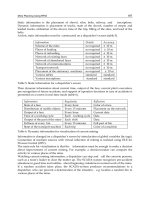
The following are the requirements associated with true 3D co-planarity measurements:
Accuracy Repeatability
Co-planarity (regression plane) 0.0002" 0.0002" 0.0004"
True position error 0.0003" 0.0003"
Pitch 0.0005" 0.0003"
Ball diameter (in the case of BGA pkg) 0.0010" 0.0003"
Board warpage 0.0003" 0.0003"
Height resolution 0.0000625"
These are three sigma-based measurements. The ideal approach should be able to handle all types of IC packages, of
which there are many.
Significantly, as noted throughout the production processes, there is a requirement for alignment. Pattern recognition
systems used are generally purchased under OEM agreements by the equipment builders and embedded in their
machines.
Another major generic application in semiconductor manufacturing is monitoring work in process inventory. This is
done based on OCR or bar-code-reading techniques. In the case of OCR, again general-purpose machine vision
systems are used.
10.2—
Electronic Manufacturing
As in semiconductors, the process begins with the creation of the circuit design using CAD systems. Using the CAD-
generated files, the artwork masters are created by computer-driven photoplotters that design and lay out the conductor
patterns.
Generally, the artwork masters are silver halide film transparencies representing an unmagnified picture of the
conductor line pattern. In some instances, glass is used in place of film where ultra high quality is required. This
practice is consistent with the use of glass reticles in IC manufacture.
The artwork master is inspected to assure it satisfies the design rules, matches the referenced image, is defect-free and
that the dimensions of the conductor paths are correct. Defects would include: mousebites, line breaks, pinholes, or
other blemishes on the conductor pattern that would be reproduced on pho-
Page 245
totools or production boards. Dust, dirt and scratches on the artwork will produce rejects.
Measuring the dimensions of the artwork is sometimes done with machine-vision-based off-line gauging stations. The
phototools or the working artwork films are then produced from the master artwork. The phototools are used to
actually transfer the conductor line circuit print to the PC board. A photographic exposure process makes the transfer.
The phototools are silver halide or diazo transparencies that are prepared by a standard contact printing process from
the artwork master.
Inspection of these phototools is just as extensive and detailed as that of the master artwork. It is of prime importance
because the next step in the process is to transfer the print to the actual board. If defects are made in this sequence, they
must be found before the inner layers are laminated together in the case of multilayer boards. The same equipment that
is used to inspect the master artwork is used to inspect the phototools, again for pattern correctness, dimensions and
defects.
Along a parallel production path the base laminate material is being prepared. The inner layers are actually discrete
sheets of laminate material, the substrate being plastics such as polymide, epoxy/glass or teflon-based laminates,
usually 0.003'', or greater. Any number of products known as web scanners can inspect the substrate materials at their
point of manufacture.
The laminate is generally a continuous coil stock so the first operation is a shearing one to produce the discrete layer.
In some cases, holes are drilled into the substrate and machine-vision-based hole inspection can be done to verify
presence, location and completeness of holes.
A deburring or desmearing operation might follow. Electroless copper is then deposited. The holes are inspected to
assure plating coverage, generally using a microsectioning on a sample basis or magnifying glass.
The next production process is exposure and development. The conductor pattern is transferred to the inner layers.
Once again the pattern should be inspected closely to determine if there are any defects that can be touched up and
repaired.
The substrate may be laminated to a thin copper sheet. The copper clad laminate is overcoated with photoresist and has
the conductor pattern exposed on it. Again, inspection is important at this stage because many defects which may have
been caused by defects that were in the photoresist pattern can be corrected. The same equipment used to inspect the
phototools can be used to perform this inspection as well.
Copper and tin plating operations may be performed at this time and the resist stripped to get rid of excess material. At
this point in the process, the board is acid-etched to create the conductor pattern in the copper. This is a critical
inspection point, because after this inspection the layers will be laminated together and defect correction is difficult if
not impossible.
Page 246
Some time ago it was analyzed that to repair the artwork only costs $.25; to repair the inner layer, about $2.50; to
repair a multilayer board for an inner layer defect, about $25; to repair a populated board for an inner layer defect,
about $250.
Bare board inspection (Figure 10.3) is made for conditions such as: line breaks/opens could be caused by flaking
photoresist or by a scratch in the artwork; short, often caused by underetch or a blob of excess copper; pinhole, often
shows up in a pad and can be caused by a thin area in the copper cladding; overetch, can create narrow conductor lines;
underetch, can create thick conductor lines and leave excess copper; excess copper, can be attached to the circuit
pattern where it can affect the performance of the board, or be separate from the pattern (both should be removed);
mousebite or gouge out of a line, a thin area of line.
Figure 10.3
Bareboard inspection system offered by AOI Systems.
At this stage the inner layers are laminated together (if multilayer). In the case of multilayered boards, the outer layer
of the board is then processed. The same steps as enumerated above are followed: exposure and development etch and
strip. The multilayered boards have pad holes drilled in them so leads of components can be inserted into the boards.
These drilling machines may use X-ray-based imaging systems and machine-vision-based pattern recognition systems
to align the boards to assure correct hole drilling.
It is noted that in some cases X-ray inspection equipment is used in the artwork compensation process, typically when
hole sizes exceed pad size tolerances. This is done on a sample at the beginning of a run. Based on registration
measurements obtained from the 'first piece', a program can be generated that compen-
Page 247
sates the original coordinates with dimensional offsets which are used during subsequent hole drilling.
The holes are through-plated to assure perfect contacts. Again visual inspection is performed and, on a sample basis,
microsectioning is performed to verify reliability of the plating process. Connector fingers may also be plated at this
time. Special machine-vision-based systems have been built to perform some of this inspection.
It is noted that wherever plating is performed, coating thickness can be measured using any number of techniques: X-
ray fluorescence, eddy current, magnetic induction, Beta backscatter, and microresistance.
At this stage, the inspection process is complicated by the presence of holes drilled in the boards, which leads to a
potential defect called "breakout." When holes are drilled in the pads at the end of a conductor line, they leave an
annular ring around the hole. If the line is slightly out of alignment, or slightly short or long, the drill will be off center
and the hole will cut the annular ring causing "breakout."
X-ray systems permit the detection and measurement of: inner-layer shifts, pad registration, breakout measurement,
drill offset, contamination and shorting. Real-time X-ray systems are those that have replaced film with a display
viewed by an operator to provide immediate decision. In some cases the systems can do some image processing to
enhance the images.
At this time, solder reflow and solder mask operations are performed. The solder mask is generally applied using
screen-printing techniques. Next, there is a final inspection and most likely an electrical test. Machine-vision-based
inspection of solder mask has also been offered; however, there may currently be limits to the effectiveness of the
system given the complexity of the appearance variables.
Today automatic optical inspection (AOI) techniques employing machine-vision-based approaches are in widespread
use throughout the bare board manufacturing cycle, especially in the manufacture of high value, multilayered boards.
Specifically, AOI is used after the following operations:
Artwork masters and production phototools
Inner and outer layers after development
Inner layers after etch and strip
Outer layers after reflow
Significantly, after reflow the application is especially challenging for three reasons: 1) the holes make it necessary to
inspect the annular rings for width and breakout; 2) the reflective characteristics of reflowed solder are quite different
from those of bare copper and 3) whereas the copper surface is flat, the reflowed solder surface is curved, making it
difficult to properly gage the width of the conductor using specular reflection. It is noted that after reflow is the last
point at which repairs can be made to the conductor pattern.
Page 248
A final inspection after routing and solder masking may be performed for cosmetic defects primarily. Defects in the
conductor pattern are difficult to find because the solder mask obscures the conductors. Significantly, automating this
visual inspection is difficult because of the wide variations in appearance in the solder mask itself, due to all the
"background noise" stemming from the patterns on the board - conductors and markings.
Preloaded Board Inspection (warpage) - Some companies have suggested a need to determine board warpage and
verify hole presence and completeness. Speeds on the order of 9 square feet/minute are desired. This appears to be
more of a diagnostic tool to assess the effects of board materials and board designs by checking board warpage on a
populated printed circuit board before and after soldering operations. They suggest that this approach permits local
evaluation of board warpage versus global evaluation. This way they can adjust tolerances to be part specific. For
example, a BGA may require a warp spec of 0.5% across the interconnect area. However, to ensure good
interconnection otherwise a 0.5% tolerance may be required across the entire board, whether such flatness is necessary
beyond the BGA or not. With their system a 0.5% tolerance can be set in the BGA area only.
The population or assembly of the printed circuit board is generally performed at a completely different facility
from the one that manufactures the bare board. The requirements for inspection depend on the board design itself - lead
through hole (LTH) components, surface mount device (SMD) components, or mixed (Figure 10.4).
Where companies are producers of lower volumes but high product mixes, robotic-based assembly machines with their
inherent flexibility are used. These generally use machine-vision-based motion servoing.
In the case of LTH, the first inspection is performed after the board has been populated and before soldering.
Inspection is for: presence of lead in correct hole, verification of clinch, and in some cases, lead length.
After soldering, inspection can also be performed by equipment from these same companies or from companies that
use X-ray based approaches for solder joint inspection with automated image processing.
In fabricating SMD boards, solder paste or epoxy must first be applied to the pads. Solder paste is generally applied
using screen-printing techniques. The more automated screen printers employ machine vision servoing based on
monitoring fiducials. In some cases this is an aid in set up. In other cases the capability is embodied in the screen
printer for ongoing correction for screen stretch, etc. While the products that are usually offered for fiducial finding are
used on an OEM basis by the screen printers, a leading supplier of such systems for the screen printer niche is ORS
automation.
Immediately after screen printing, either on-line or off-line, an inspection is performed to verify presence, placement
and, in some cases, volume. While this may be an on-line operation, it is unlikely to be done on a 100% basis because
of