Microsensors, MEMS and Smart Devices - Gardner Varadhan and Awadelkarim Part 5 pdf
Bạn đang xem bản rút gọn của tài liệu. Xem và tải ngay bản đầy đủ của tài liệu tại đây (2.59 MB, 30 trang )
MONOLITHIC MOUNTING
103
Al
or Au
wire
Die or
chip
Die-bond
material
Figure
4.38 Die-
and
wire-bonding
technique
-TAB lead
—
Chip
•
Die-bond
material
Substrate
\
Figure
4.39
Tape-automated
bonding technique
hot
thermode produces
a
faster throughput than wire bonding. Moreover,
the
reduced
inductance
of a
probe means that
the
devices
can be
AC-tested.
The
disadvantages
of TAB
include
the
relatively high cost
of the
process
and the
need
for a
large device footprint. This problem
is
overcome
in flip-chip
mounting.
4.4.3 Flip
TAB
Bonding
In
flip TAB
bonding,
the die is
mounted upside down
on the
substrate,
as
shown
in
Figure 4.40.
The
major advantage
of flip TAB
over regular
TAB
mounting
is
that
the die
can
be
subsequently attached
to a
metal
lid for
better thermal management.
4.4.4 Flip-Chip
Mounting
Finally,
flip-chip
mounting
of the die has a
number
of key
advantages.
It
provides
an
excellent contact between
the die and
substrate
by
eliminating
the
wire
or
beam lead
Chip
Flip
TAB
lead
Support material
Substrate
Figure
4.40
Flip
TAB
technique
104
STANDARD MICROELECTRONIC TECHNOLOGIES
Chip
—
Solder
bumps
""
Substrate
Figure
4.41
Flip-chip
mounting technique
entirely (see Figure
4.41).
Solder bumps
are
placed
on the
substrate
and
then
the die is
mounted
facedown,
and the
solder
is
melted
to
make
the
connection.
The
small
footprint
and
pitch, coupled with short interconnect
of
about
50
urn,
and
hence
low
inductance,
make this
a
very attractive technology
at a
relatively
low
cost.
Full
details
of
these bonding methods
may be
found
in
textbooks such
as
Doane
and
Franzon
(1993).
4.5
PRINTED CIRCUIT BOARD TECHNOLOGIES
Once electronic components have been made
and
packaged, such
as the
monolithic
ICs
described
in
Sections
4.3 and
4.4, they need
to be
connected
with
other components
to
form
a
circuit board.
The
most common
way to do
this
is to
make
a
PCB, which
is
also
known
as a
printed wiring
board
(PWB).
There
are a
number
of
different
PCB
technologies based
on
different
dielectric materials
and
their fabrication
process.
Here,
we
consider
the
three main kinds
of
organic PCBs
-
solid,
flexible, and
moulded;
the
ceramic
PCB is
known
as a
thick
film
hybrid circuit board
and is
discussed
in
Section
4.6.1.
4.5.1 Solid Board
Solid (and
flexible)
PCBs generally consist
of an
organic dielectric material
on top of
which
is a
thin metal layer
-
predominantly
copper.
The
copper layer
is
patterned using
a
photoresist
material
and an
acid
etch
to
define
the
tracks between
the
electronic
compo-
nents.
In the
case
of
surface-mount devices,
a
single-sided organic
PCB can be
used
as
illustrated
in
Figure 4.42(a). Single-sided PCBs
are
simpler
to
make
and are
increasingly
used with
the
greater availability
of
surface-mount components. However,
the
majority
of
organic
PCBs
are
double-sided
with multilayer
boards
used
in
special
cases,
such
as the
need
to
introduce ground planes
and
thereby reduce
the
electrical interference between
high-speed switching logic
and
analogue circuitry (Figure 4.42(b)
and
(c)).
A
double-
sided
PCB has
copper
tracks patterned
on
both
sides
of the
dielectric material. Electrical
connections between
the
layers
are
formed
by
drilling holes through
the
board,
and
this
is
followed
by the
plating
of the
sides
of the
holes. Clearly,
the
metal
will
be
thinner
here,
and
passing large currents down through
holes
can be a
problem. Finally,
a
solder
mask
is
prepared and,
if
required,
a
protective layer
is
patterned, leaving just
the
solder areas
exposed.
In
a
solid
organic PCB,
the
dielectric material consists
of an
organic resin reinforced
with
fibres.
The
fibres
are
either chopped
or
woven into
the
fabric,
and the
liquid
resin
is
added
and
processed using heat
and
pressure
to
form
a
solid sheet.
The
most
PRINTED CIRCUIT BOARD TECHNOLOGIES
105
-
Copper
interconnect
Dielectric
-Plated
through
hole
(b)
L
—Dielectric
Copper
interconnect
Blind
via —\
/-Buried
via
Dielectric-/
Copper interconnect-
(c)
Plated
through
hole
Figure
4.42
Schematic
cross
section
of
three types
of
organic
PCBs:
(a)
single-sided;
(b)
double-sided;
and (c)
multilayered
Table
4.8
Material
properties
of
some
common
fibres
used
in
organic
PCBs
Thermal
expansion
Dielectric constant
at 1 MHz
Dissipation
factor
at 1 MHz
Maximum
elongation
Softening temperature
Specific gravity
Specific
heat capacity
Tensile
strength
Thermal conductivity
Young's modulus
Units
ppm/°C
-
10
–3
%
°c
g/cm
3
J/g.°c
kg/mm
W/m.°C
kg/mm
e-glass
5.0
5.8
1.1
4.8
840
2.54
0.827
350
0.89
7400
s-glass
2.8
4.52
2.6
5.5
975
2.49
0.735
475
0.9
8600
Quartz
0.54
3.5
0.2
5.0
1420
2.20
0.966
200
1.1
7450
Aramid
–5.0
a
4.0
1.0
4.5
300
1.40
1.092
400
0.5
13000
a
Along
axis
of
fibre;
radial
is 60
ppm/°C
commonly
used
fibres
are
paper, e-glass, s-glass,
quartz,
and
aramid.
The
precise choice
of
the
dielectric material depends
on the
technical demands presented
by the
device
and
application proposed,
and the
properties, such
as the
permittivity
and
loss factor,
are
frequently
the
most important. Table
4.8
gives some
of the
properties
of the
fibres
that
are
commonly
used
in
organic PCBs.
4.5.2 Flexible Board
In
flexible
PCBs,
the
resin used
to
make
a
solid dielectric material
is
replaced
by a
thin
flexible
dielectric material
and the
metal
is
replaced
by a
ductile copper foil. Again,
a
106
STANDARD
MICROELECTRONIC
TECHNOLOGIES
Etch
Laminate
Cover
film
Adhesive
|
Etch
Copper
Adhesive
Base
film
Cover film
Adhesive
Copper
Adhesive
Base
film
Adhesive
Copper
Adhesive
Cover film
Cover
film"
Adhesive
Copper
Adhesive
Base
film
Adhesive
Copper
Adhesive
Cover film
Adhesive
Copper
Adhesive
Base film
firm
firm
mm nrm
Single-sided
flex-printed
wiring
:>
nrm
mm mm mm
Y///////////////////////////A
mm
mm mm mm
Y///////////////////////////A
Double-sided
flex-printed
wiring
Etch
Laminate
mm
rmn mm nrm
nrm
mrn rmn mm
mm
mm mm mm
y/////////////////////////zm
Multilayer
flex-printed
wiring
Figure
4.43 Schematic cross section
of
three types
of flexible
PCBs:
(a)
single-sided;
(b)
double-sided;
and (c)
multilayered
Table
4.9
Material properties
of
some resins used
in
organic PCBs
CTE
Dielectric constant
at
1 MHz
Poisson's
ratio
Temperature
Thermal conductivity
a
Young's
modulus
Units
ppm/°C
-
-
°C
W/m.°K
GPa
Epoxy
58
4.5
0.35
130
0.3
3.4
Polyimide
49
4.3
0.33
260
0.3
4.1
Cyanate
ester
55
3.8
0.35
260
0.3
3.4
PTFE
99
2.6
0.46
-
0.3
0.03
a
Approximate values
number
of
different
organic materials
can be
used
to
make
a
flexible wiring board such
as
polyimide (Kapton), polyester terephthalate (Mylar), random
fibre
aramid (Nomex),
Teflon,
and
polyvinyl chloride (PVC).
The
copper
foil
is
processed
as
before
by
optical
lithography,
and
layers
can be
joined together
to
form
multilayer laminates.
The
layers
are
usually
bonded together
using
an
adhesive such
as
acrylic, epoxy, polyester,
and
PRINTED
CIRCUIT
BOARD
TECHNOLOGIES
107
Table
4.10
Material
properties
of
some
dielectric
films
used
in flexible
organic
PCBs
Density
Dielectric
constant
at
1
MHz
Dielectric
strength,
min.
Dimensional
stability,
max.
Dissipation
factor
at
1
MHz
Elongation,
min.
Initial
tear
strength
Tensile
strength,
min.
Volume
resistivity
(damp
heat)
Units
Polyimide
g/cm
3
1.40
4.00
kV/mm
79
%
0.15
10
–3
12
%
40
g
500
MPa 165
Q-cm 10
6
FEP
2.15
2.30
79
0.3
0.7
200
200
17
10
7
Polyester
1.38
3.40
79
0.25
7.0
90
800
138
-
Epoxy
polyester
1.53
-
5.9
0.20
0
15
1700
34
10
5
Aramid
paper
0.65
3.00
15.4
0.30
10
4
-
28
10
6
polytetrafluroethylene
(PTFE). Figure 4.43 shows
the way in
which single-sided, double-
sided,
and
multilayer
flexible
PWBs
are
constructed.
Table
4.9
gives some typical properties
of the
resins used
in flexible
organic PCBs.
Care
is
needed
to
match these properties with those
of the
copper layer
and the
nature
of
the
circuit,
for
example, high frequency
or
high power.
Flexible
PCB
dielectric
and
adhesive
films are now
manufactured
to a
standard,
and
Table 4.10 shows
the
Class
3
properties
of
some dielectric
films
according
to the
standard
IPC-FC-231.
Accordingly, organic
PCB
laminates
can now be
constructed
with
increased
confidence
in
their
performance.
4.5.3
Plastic Moulded
The
most common forms
of PCB - the
organic
PCB and the
ceramic
PCB
(see next
section)
- are
planar, that
is, the
metal interconnects
are
formed
in two
dimensions with
plated through holes joining
one
layer
to
another. However,
it is
possible
to
make
a
three-dimensional
PCB by the
moulding
of a
suitable plastic.
A
three-dimensional
PCB
can
be
made
from
extruded
or
injection-moulded thermoplastic resins with
a
conductive
layer
that
is
selectively applied
on its
surface. However, high-temperature thermoplastics
are
required
to
withstand
the
soldering
process,
and
commonly used materials
are
polyethersulfone, polyetherimide,
and
polysulfone. Plastic moulded PCBs have several
advantages
over organic PCBs, such
as
superior electrical
and
thermal properties
and
the
ability
to
include
in the
design, noncircular holes, connectors, spacers, bosses,
and
so
on.
More
often
than
not,
a
moulded
PCB is in
essence
an IC
chip carrier package.
Plastic
moulded PCBs
may
prove
to be
advantageous
in
microtransducers
and
MEMS
applications,
in
particular,
when
the
assembled microstructure
has an
irregular
structure
or
needs special clips
or
connectors.
The
plastic moulded
IC
package
may
also
be
used
as
part
of a
hybrid MEMS before
full
integration
is
realised.
Future
Micro-moulds
may
be
fabricated
using
microstereolithography (see Chapter
7).
108
STANDARD MICROELECTRONIC TECHNOLOGIES
4.6
HYBRID
AND MCM
TECHNOLOGIES
4.6.1 Thick Film
PCBs
can
also
be
formed
on a
ceramic board,
and
these
may be
referred
to as
ceramic
PCBs.
A
ceramic board, such
as
alumina,
offers
a
number
of
advantages over
organic PCBs, because
a
ceramic board
is
much more rigid, tends
to be
flatter,
has a
lower
dielectric
loss,
and can
withstand higher
process
temperatures.
In
addition, alumina
is a
very inert material
and
hence
is
less prone
to
chemical attack than
an
organic PCB.
Ceramic PCBs
can be
processed
in a
number
of
different
ways, such
as
thick-film, thin-
film,
co-fired,
and
direct-bond copper.
The
most important technology
is
probably
the
thick
film.
Circuit boards have been made
for
more than
twenty
years
using
this technology
and
are
usually referred
to as
hybrid
circuits.
In
thick-film technology,
a
number
of
different
pastes have been developed (known
as
inks),
and
these pastes
can be
screen-printed onto
a
ceramic base
to
produce interconnects,
resistors, inductors,
and
capacitors.
Example:
1.
Artwork
is
generated
to
define
the
screens
or
stencils
for the
wiring layers, vias,
resistive layers,
and
dielectric
layers.
2.
Ceramic substrate
is cut to
size using
laser
drilling,
and
perforations that
act as
snapping
lines
are
included after
the
process
is
complete.
3.
Substrate
is
cleaned using
a
sandblaster,
rinsed in hot
isopropyl alcohols,
and
heated
to 800 to 925 °C to
drive
off
organic contaminants.
4.
Each layer
is
then
in
turn
screen-printed
to
form
the
multilayer structure. Each paste
is
first
dried
at 85 to 150 °C to
remove volatiles
and
then
fired at 400 to
1000
°C.
5. The
last high-temperature process performed
is the
resistive layer (800
to
1000 °C).
6. A
low-temperature glass
can be
printed
and fired at 425 to 525 °C to
form
a
protective
overlayer
or
solder mask.
Thick-film technology
has
some
useful
advantages over other types
of PCB
manufacture.
The
process
is
relatively simple
- it
does
not
require expensive vacuum equipment (like
thin-film
deposition)
- and
hence
is an
inexpensive method
of
making circuit boards.
Figure 4.44 shows
a
photograph
of a
thick-film
PCB
used
to
mount
an
ion-selective
sensor
and the
associated
discrete electronic circuitry (Atkinson
2001).
The
thick-film
process
is
useful
here
not
only because
it is
inexpensive
but
also
because
it
forms
a
robust
and
chemically inert substrate
for the
chemical sensor.
The
principal disadvantage
of
thick-
film
technology
is
that
the
packing density
is
limited
by the
masking accuracy
-
some
hundreds
of
microns. Photolithographically patterned
thin-film
layers
can
overcome this
problem
but
require more sophisticated equipment.
4.6.2 Multichip Modules
Increasingly,
PCB
technologies
are
being used
to
make multichip modules (MCMs).
A
multichip module
is a
series
of
monolithic chips
(often
silicon) that
are
connected
and
HYBRID
AND MCM
TECHNOLOGIES
109
Figure
4.44
ISFET
sensor
and
associated circuitry mounted
on a
ceramic (hybrid) PCB. From
Atkinson
(2001)
250
200
100
50
0
PCB
SMT
brids
50
microns
HDMI
25
microns
HDMI
10
microns
HDMI
0
WSI
50
Silicon
efficiency
(%)
Figure
4.45
Silicon
efficiency rating
and
line width
of
different interconnection
and
substrate
technologies.
After
Ginsberg (1992)
packaged
to
make
a
self-contained
unit.
This module
can
then
be
either connected directly
to
peripheral ports
for
communication
or
plugged into another PCB.
One
important reason
for
using
MCM
instead
of a
conventional die-packaging approach
is
that
the
active silicon
efficiency
rating
is
improved (see Figure
4.45).
In
other words,
the
total area
of the
semiconductor
die is
comparable
to the MCM
substrate area.
As can be
seen
from
the
figure,
conventional
PCB
technologies
and
even
SMT and
hybrid
are
much
poorer
than
the
high-density
MCM
methods.
The
ceramic-based technology
is
referred
to as an
MCM-C
structure; other MCM-C
technologies include high-temperature co-fired ceramic (HTCC)
and
low-temperature
co-
fired
ceramic (LTCC). Table 4.11 lists
the
relative merits
of
different
MCM-C technologies.
110
STANDARD
MICROELECTRONIC TECHNOLOGIES
Table
4.11
Relative merits
of
MCM-C technologies,
with
one
being
the
best
Adapted
from
Doane
and
Franzon
(1993),
Property
Top-layer dimensional
stability
Low K
values
High-conductivity
metallisation
High mechanical strength
High
thermal
conductivity
CTE
matched
to
alumina
or
silicon
Hermeticity
Excellent
dielectric
control
Surface
roughness
Thick-film
1
1
1
2
2
2
2
3
3
HTCC
3
3
3
1
1
3
1
1
2
LTCC
2
1
1
3
3
1
1
1
1
Benefit
Improved wire-bond,
assembly yield stability
Improved high-frequency
performance
Smaller line
and
space
designs
More rugged package
Good thermal characteristics
Capability
of
assembly
Development
of
packages
More consistent electrical
performance
Better high-frequency
performance
Table
4.12
Properties
of
some commonly used MCM-C materials. Adapted
from
Doane
and
Franzon (1993)
Property
Purity
Colour
CTE at 25 to
400°C
Density
Dielectric constant
at
1
MHz
Dielectric
loss
tangent
at
1 MHz
Dielectric strength
Flexural strength
Resistivity
Specific heat capacity
Thermal conductivity
Units
%
-
10-
6
/°C
g/cm
3
-
10
–3
kV/mm
GPa
ft-cm
J/g.°K
W/m.°K
AI
2
O
3
99.5
White
7.6
3.87
9.9
0.1
24
400
10
14
-
20-35
AI
2
O
3
96
White
7.1
3.7
9.5
0.4
26
250
10
14
-
20-35
BeO
99.5
White
9.0
3.01
6.5
0.4
9.5
170-240
10
15
-
250-260
A1N
98-99.8
Dark
grey
4.4
3.255
8.8-8.9
0.7-2.0
10-14
280-320
>10
13
0.74
80-260
The
choice
of
ceramic substrate
is
important
and the >99
percent alumina
has a low
microwave
loss,
good strength
and
thermal conductivity,
and
good
flatness.
However,
it is
expensive
and 96
percent alumina
can be
used
in
most applications.
In
cases
in
which
a
high thermal conductivity
is
required (e.g. power devices), beryllia (BeO)
or
aluminum nitride (A1N)
can be
used, although these involve
a
higher cost. Table 4.12
summarises
the key
properties
of the
ceramic substrates.
In
addition, modules wherein interconnections
are
made
by
thin
films are
classified
as
MCM-D
and
those made
by
plastic (organic) laminate-based technologies
are
classified
as
MCM-L. Table 4.13 shows
a
comparison
of the
typical properties
of the
three main
types
of MCM
interconnection technologies.
HYBRID
AND MCM
TECHNOLOGIES
111
Table
4.13
Comparison
of MCM
interconnection technologies.
(1993)
Property
MCM
class
Dielectric
material:
Dielectric constant
Thickness/layer (um)
Min.
via
diameter (urn)
Conductive
materials:
Thickness
(am)
Line width
(um)
Line pitch
(um)
Bond
pad
pitch
(um)
Maximum
number
of
layers
Electrical
properties:
Line resistance
(£2
-cm)
Sheet resistance (mfi/sq)
Propagation delay
(ps/cm)
Stripline capacitance
of
50 Q
line (pF/cm)
Thick film
MCM-C
Glass-ceramic
6-9
35-65
200
Cu
(Au)
15
100-150
250-350
250-350
5
to 10+
0.2-0.3
3.0
90
4.3
HTCC
MCM-C
Alumina
9.5
100-750
100-200
W(Co)
15
100-125
250-625
200-300
50+
0.8-1
10.0
102
2.1
Adapted
from
Doane
and
Franzon
Thin
film
MCM-D
Polyimide
3.5
25
25
Cu
(Al,
Au)
5
10-25
50-125
100
4-to
10
1.3-3.4
3.4
62
1.25
Laminate
MCM-L
Epoxy-glass
4.8
120
300
Cu
25
75-125
150-250
200
40+
0.06-0.09
0.7
72
1.46
MCM
technology
has
several advantages
for
integrating arrays
of
microtransducers
and
even
MEMS (Jones
and
Harsanyi 1995). First,
the
semiconductor dies
can be
fabricated
by
a
different
process, with some dies being precision analogue (bipolar) components
and
others being digital (CMOS) logic components. Second,
the
cost
of
fabricating
the MCM
substrate
is
often
less expensive than using
a
silicon process,
and the
lower
die
complexity
improves
the
yield. Finally,
the
design
and
fabrication
of a
custom ASIC chip
is a
time-
consuming
and
expensive business.
For
most sensing technologies, there
is a
need
for new
silicon
microstructures, precision analogue circuitry,
and
digital readout. Therefore, fabri-
cating
a
BiCMOS ASIC chip that includes bulk-
or
surface-micromachining techniques
is
an
expensive
option
and
prohibitive
for
many
applications.
Figure
4.46
shows
the
layout
of a
multichip module (MCM-L)
with
the TAB
patterns
shown
to
make
the
interconnections
(Joly
et al.
1995).
This
MCM-L
has
been
designed
for
a
high-speed telecommunications automatic teller machine (ATM) switching module,
which,
with
a
power budget
of 150 W, is a
demanding application.
4.6.3 Ball Grid Array
There
are a
number
of
other specialised packaging technologies that
can be
used
as an
alternative
to the
conventional
PCB or
MCM.
The
main drive
for
these
technologies
is
to
reduce
the
size
of the
device
and
maximise
the
number
of
I/Os.
For
example, there
are
three types
of
ball grid array (BGA) packages. Figure
4.47
shows these three types:
the
plastic
BGA,
ceramic
BGA,
and
tape
BGA.
The
general advantages
of BGA are
the
smaller package size,
low
system cost,
and
ease
of
assembly.
The
relative merits
of
112
STANDARD
MICROELECTRONIC
TECHNOLOGIES
Figure
4.46
Example
of a
high-density
MCM-L
substrate
with
TAB
patterns.
From
Joly
et al.
(1995)
plastic
and
ceramic
PGA
packages
are
similar
to
those already discussed
for
PCBs
and
MCMs.
The
tape
EGA
uses
a
TAB-like
frame
that connects
the die
with
the
next
layer
board.
4.7
PROGRAMMABLE
DEVICES
AND
ASICs
The
microtechnologies described
in
this chapter
are
used
to
make
a
variety
of
different
microelectronic components. Figure 4.48 shows
the
sort
of
devices
that
can be
made
today.
These
are
subdivided into
two
classes
-
standard components, which
are
designed
for
a fixed
application
or
those that
can be
programmed,
and
application-specific
ICs
(ASICs),
which
are
further
subdivided.
The
standard components
that
may be
regarded
as
having
fixed
application
are
discrete devices (e.g. n-p-n transistors), linear devices (e.g.
operational amplifiers),
and IC
logic
families
of TTL and
CMOS (e.g. logic
gates
and
binary
counters, random
access
memory).
The
other types
of
standard component
may be
classified
as
having
the
application defined
by
hardware
or
software programming.
In
hardware programming,
the
application
is
defined
by
masks
in the
process,
and
examples
of
these
devices
include programmable logic arrays (PLAs)
and
read-only
memory
(ROM) chips. There
has
been
a
move
in
recent years
to
make
software
programmable components.
The
most familiar ones
are the
microprocessors (such
as the
Motorola
68 000
series
or
Intel
Pentium)
that
form
the
heart
of a
microcomputer
and its
PROGRAMMABLE
DEVICES
AND
ASICs
113
Figure
4.47
Three
main
types
of
ball
grid
array
packages:
(a)
plastic;
(b)
ceramic;
and (c)
tape-ball
nonvolatile memory.
For
example,
erasable
programmable read-only memory (EPROM)
in
which
the
memory
is
erased
by UV
light
and its
easier-to-use successor, electronically
erasable programmable read-only memory (EEPROM).
In
recent years, there
has
been
a
strong
move toward software programmable array devices; these components
do not
have
the
mathematical capability
of a
microprocessor
but are
able
to
perform simple logical
actions.
As
such,
they
can be
high-speed stand-alone chips
or
glue chips
-
that
is,
chips
that
interface
an
analogue device with
a
microcontroller
or
communication chip. Examples
of
these
are
programmable
logic
devices
(PLDs)
and
PGAs that
may
have several thousand
114
STANDARD
MICROELECTRONIC TECHNOLOGIES
gates
to
define.
The
newest type
of
component
is the
programmable analogue array (PAA)
device,
and
these
may
well become increasingly important
in
sensing applications
in
which
the
design
of an
operational amplifier circuit
can be set and
reset
through
I/O
ports.
It
should
be
noted that this classification
of
devices into hardware
and
software
programming
is not
universally accepted. Sometimes,
it may be
more
useful
to
distinguish
Standard devices
Standard components
Application-specific
ICs
Fixed
Applications
application
by
programming
1
Discrete
Log
fam
n
O
1
1
1
ic
Hardware
Software
lies programming programming
(MASK)
1
"L
PLA
Microprocessor
MOS ROM
EPROM, EEPROM
PLD, PGA,
AA
Semicustom
Full Silicon
custom compilation
ill I
Gate Analogue Master Standard
array
array
slice
cell
Figure 4.48 Manufacturing methods
for
common microelectronic
devices
and ICs
Increasing
risk
Increasing
density
Increasing
time
to
market
Increasing
versatility
Increasing
development
cost
V
Decreasing
cost/gate
Figure
4.49 Diagram showing
the
various trade-offs between
the
different
technologies
adopted
to
make
an
ASIC
chip
PROGRAMMABLE
DEVICES
AND
ASICs
115
between
devices according
to
where they were programmed.
In
this case, devices
may
all be
regarded
as
'electrically'
programmed
and
then they
can be
subdivided into
those
programmed
by the
manufacturer
(as in
mask-programmed parts)
and
those programmed
by
the
user
(as in field-programmable
gate array).
The
second class
of
components
are
those called
application-specific
integrated circuit
ICs
(ASICs)
(see Figure
4.48).
There
are
several types
of
ASIC
and
these
are
referred
to
as
full-custom, semicustom,
and
silicon compilation. Full-custom ASICs
are
those that
are
defined
down
to the
silicon
level
and, therefore, there
is
great
scope
for the
optimisation
of
the
device layout, reduction
in
silicon
die
area,
and
speed
of
operation. However,
a
full-custom
design
can be an
expensive option
and is
only
useful
for
large volumes.
Silicon compilation
is the
exact opposite; hence,
it is
rather
wasteful
of
silicon
and
pushes
up
the
process costs while minimising
the
design cost.
The
more common approach,
and
more relevant
for the
manufacturing
of
microtransducers,
is
that
of a
semicustom ASIC
chip.
This
has
four
subdivisions.
In
gate arrays,
the
device
has
been partly processed
and
the
designer simply
defines
the
interconnection
of the
digital logic devices
by one
or two
customised masks. Thus, most
of the
process
is
common
to a
number
of end
users,
and
hence
the
costs
are
greatly reduced.
In
analogue arrays,
the
same principle
is
applied,
except
that this time
a
range
of
analogue components
are
being connected
and
an
analogue circuit
is
formed.
In
master slice,
the
wafer
run can be
split
at a
later stage
into
different
subprocesses.
The
last type
of
semicustom approach
is the
standard cell
in
which
the
designer selects standard logic
or
analogue circuit
functions
from
a
software
library
and
then connects them together
on the
silicon die.
The
design time
is
reduced
by
using
standard
cells
with
a
standard
process.
The
various trade-offs
of the
ASIC technologies
are
illustrated
in
Figure 4.49 such
as
risk, cost, density,
and
flexibility.
Strictly speaking, PLDs
are not
ASICs
but
they
have
been included here because they
are
often
the
main competitors
to an
ASIC chip.
Although
the
number
of
equivalent gates
per
chip
in
PLDs
is
only
500 to
3000,
the
cost
advantage
is
often
attractive.
When
deciding
upon which ASIC technology
to
use,
it is
important
to
weigh
the
relative
costs involved, such
as the
development time
and the
nonrecurring engineering costs (mask
making
etc.),
and
design consideration
such
as the
architecture required
and the
number
of
gates.
In the final
analysis,
it is
usually
the
volume
that
dictates
the
cost
to
manufacture
the
chips;
the
production charges
per
1000
gates
are
shown against total volume
in
Table 4.14.
For
example, modern
microprocessor
and
memory chips
are
manufactured
in
enormous
volume
(millions
of
chips
per
year)
and so the
cost
is
dominated
by the
time
to
process
and,
hence,
the
size
of
wafer
processed.
Current microelectronic plants
use
wafers
of a
diameter
of 8" or
more,
and
companies have
to
build
new
plants that cost nearly
one
billion
dollars
as
larger
diameter wafers
become
available.
This situation
is
usually
not
applicable
to the
manufacture
of
microsensors
because
of the
much reduced volume
and
higher added
value.
However,
all of
these production costs
per
kgate
are low
compared with
the
cost
of
fabricating
a
nonstandard component.
For
instance, when integrating
a
microtransducer
or
MEMS with
a
standard
IC, it is
nearly always necessary
to
develop nonstandard pre-
or
postprocessing steps, such
as
surface
or
bulk micromachining (see next chapter). This
cost
issue
is
critical
for the
eventual success
of a
component
on the
market
and
therefore,
we
will return
to it
later
on in
Chapter
8,
having
first
described
the
different
fabrication
methods
and
technologies associated with microtransducers
and
MEMS.
116
STANDARD
MICROELECTRONIC TECHNOLOGIES
Table 4.14 Typical
costs
of
different
ASIC (and programmable device) technologies. Adapted
from
Ginsberg
(1992)
Device
Full
custom
Standard
and
compiled cells
Gate
arrays
PLDs
FPGAs
Capability
RAM,
ROM,
Analogue
RAM,
ROM,
Analogue
Logic
only
Fixed
logic
Fixed
logic
Density
(kgates)
1-100
1-10
a
1-50
1-50
0.5
1-3
Development
time
Long
Moderate
Moderate
Short
Moderate
NRE
costs
(k€)
50
15
a
-50
15-100
<5
5-20
Production
volume
(1000s)
<2.5
2.5-10
>10
<2.5
2.5-10
>10
<2.5
2.5-10
>10
<2.5
2.5-10
>10
<2.5
2.5-10
>10
Production
cost
in k€
per
kgates
N/A 1
2-3
1
5-10
3-4
2-3
N/A
3-4
2-3
8
7
6
10-20
7-15
5-12
a
Costs
shown
for
PC-based
and
workstation-based
design,
respectively
REFERENCES
Atkinson,
J.
(2001).
University
of
Southampton,
UK.
Personal communication.
Colclaser,
R. A.
(1980).
Microelectronics
Processing
and
Device Design, Wiley
&
Sons,
New
York,
p.
333.
Doane,
D. A. and
Franzon, eds. (1993).
Multichip
Module
Technologies
and
Alternatives,
Van
Nostrand
Reinhold,
New
York,
p.
875.
Furakawa,
S.
(1985). Silicon-on-insulator:
Its
Technology
and
Applications,
D.
Reidel Publishing
Company,
Dordrecht,
p.
294.
Ginsberg,
G. L.
(1992). Electronic
Equipment
Packaging Technology,
Van
Nostrand Reinhold,
New
York,
p.
279.
Gise,
P. and
Blanchard,
R.
(1986).
Modern
Semiconductor Fabrication Technology, Prentice-Hall,
New
Jersey,
p.
264.
Harper,
C. A.
(1997).
Electronic Packaging
and
Interconnection Handbook, McGraw-Hill, USA.
Hart,
P. A. H.
(1994).
Bipolar
and
Bipolar-MOS
Integration, Elsevier
Science,
Amsterdam,
p.
468.
Joly
J.,
Kurzweil,
K. and
Lambert,
D.
(1995).
"MCMs
for
computers
and
telecom
in
CHIPPAC
programme,"
in W. K.
Jones
and G.
Harsanyi, eds.,
Multichip
Modules
with
Integrated
Sensors,
NATO
ASI
series,
Kluwer
Academic Publishers, Dordrecht,
p.
324.
Jones,
W. K. and
Harsanyi,
G.,
eds. (1995).
Multichip
Modules with
Integrated
Sensors,
NATO
ASI
series, Kluwer Academic Publishers, Dordrecht,
p.
324.
Sze,
S. M.
(1985). Semiconductor Devices, Physics
and
Technology,
Wiley
&
Sons,
New
York,
p.
523.
Udrea,
F. and
Gardner,
J. W.
(1998).
UK
Patent
GB
2321336A,"Smart MOSFET
gas
sensor,"
Published
22.7.98,
Date
of filing
15.1.97. International Publication Number:
WO
98/32009,
23
July
1998, Gas-sensing semiconductor devices.
5.1
INTRODUCTION
The
emergence
of
silicon micromachining
has
enabled
the
rapid progress
in the field of
microelectromechanical systems (MEMS),
as
discussed previously
in
Chapter
1.
Silicon
micromachining
is the
process
of
fashioning microscopic mechanical parts
out of a
silicon
substrate
or,
indeed,
on top of a
silicon substrate.
It is
used
to
fabricate
a
variety
of
mechanical
microstructures including beams, diaphragms, grooves, orifices, springs, gears,
suspensions,
and a
great diversity
of
other complex mechanical structures. These mechan-
ical structures have been used successfully
to
realise
a
wide range
of
microsensors
1
and
microactuators. Silicon micromachining comprises
two
technologies:
bulk micro-
machining
and
surface micromachining.
The
topic
of
surface micromachining
is
covered
in
the
next chapter. Further details
can be
found
in the
two-volume Handbook
of
Microlithog-
raphy,
Micromachining,
and
Microfabrication
(Rai-Choudhury 1997).
Bulk
micromachining
is the
most used
of the two
principal silicon micromachining
technologies.
It
emerged
in the
early 1960s
and has
been used since then
in the
fabrication
of
many
different
microstructures. Bulk micromachining
is
utilised
in the
manufacture
of
the
majority
of
commercial devices
-
almost
all
pressure sensors
and
silicon valves
and 90
percent
of
silicon
acceleration
sensors.
The
term bulk micromachining
expresses
the
fact
that
this type
of
micromachining
is
used
to
realise
micromechanical structures within
the
bulk
of a
single-crystal silicon (SCS) wafer
by
selectively removing
the
wafer material.
The
microstructures fabricated using bulk micromachining
may
cover
the
thickness range
from
submicrons
to the
thickness
of the
full
wafer
(200
to 500 um) and the
lateral size
ranges
from
microns
to the
full
diameter
of a
wafer
(75 to 200
mm).
Etching
is the key
technological step
for
bulk micromachining.
The
etch process
employed
in
bulk micromachining comprises
one or
several
of the
following
techniques:
1.
Wet
isotropic etching
2.
Wet
anisotropic etching
3.
Plasma isotropic etching
4.
Reactive
ion
etching (RIE)
5.
Etch-stop techniques
1
Chapter
8 is
devoted
to
this topic.
5
Silicon Micromaching: Bulk
118
SILICON MICROMACHINING:
BULK
Some
of
these etch processes have already been used
as a
standard technology
in the
microelectronics
industry,
for
example,
RIE
(Chapter
2).
In
addition
to an
etch
process,
bulk micromachining
often
utilises
wafer
bonding
and
buried oxide-layer technologies. However,
the use of the
latter
in
bulk micromachining
is
still
in its
infancy.
This chapter describes
the
commonly used bulk-micromachining processes
and
gives
a set of
worked examples
2
that illustrate
the
applications
of
each one,
or a
combination,
of
these important
processes.
The
discussion includes
the
important topics
of
etch-stops
and
wafer-to-wafer bonding.
5.2
ISOTROPIC
AND
ORIENTATION-DEPENDENT
WET
ETCHING
Wet
chemical etching
is
widely used
in
semiconductor
processing.
It is
used
for
lapping
and
polishing
to
give
an
optically
flat and
damage-free surface
and to
remove contami-
nation
that results
from
wafer
handling
and
storing. Most importantly,
it is
used
in the
fabrication
of
discrete devices
and
integrated circuits (ICs)
of
relatively large dimensions
to
delineate patterns
and to
open windows
in
insulating materials.
The
basic mechanisms
for
wet
chemical etching
of
electronic
materials were described
in
Section 2.4.
It was
also mentioned that most
of the
wet-etching processes
are
isotropic, that
is,
unaffected
by
crystallographic orientation.
However, some
wet
etchants
are
orientation-dependent, that
is,
they have
the
property
of
dissolving
a
given crystal plane
of a
semiconductor much faster than other planes (see
Table 5.1).
In
diamond
and
zinc-blende
lattices,
the
(111) plane
is
more closely packed
than
the
(100) plane and, hence,
for any
given etchant,
the
etch-rate
is
expected
to be
slower.
A
commonly used orientation-dependent etch
for
silicon
consists
of a
mixture
of
potas-
sium
hydroxide (KOH)
in
water
and
isopropyl alcohol.
The
etch-rate
is
about
2.1
um/min
for
the
(110) plane,
1.4
urn/min
for the
(100) plane,
and
only
0.003
um/min
for the
(111)
plane
at 80 °C;
therefore,
the
ratio
of the
etch rates
for the
(100)
and
(110) planes
to the
(111)
plane
are
very
high
at
400:1
and
600:1,
respectively.
Table
5.1
Anisotropic
etching
characteristics
of
different
wet
etchants
for
single-crystalline
silicon
Etchant
KOH:H
2
O
KOH
EDP
N
2
H
4
H
2
O
NH
4
OH
Temperature Etch-rate (jim/hour)
of
(°C) Si(100) Si(110) Si(111)
80
75
110
118
75
84
25-42
51
176
24
126
39-66
57
99
8
0.21
0.5
1.25
11
1
'
Appendix
M
provides
a
list
of all the
worked
examples
provided
in
this
book.
ISOTROPIC
AND
ORIENTATION-DEPENDENT
WET
ETCHING
119
(111)
- -
Resist
Figure
5.1
Anisotropic etching
of
(100) crystal silicon
Figure
5.1
shows
orientation-dependent
etching
of
(100)-oriented
silicon
through pat-
terned
silicon
dioxide
(SiO2), which acts
as a
mask.
Precise
V-grooves,
in
which
the
edges
are
(111)
planes
at an
angle
of
approximately
55°
from
the
(100) surface
3
,
can be
realised
by
the
etching.
If the
etching
time
is
short,
or the
window
in the
mask
is
sufficiently
large,
U-shaped
grooves
could also
be
realised.
The
width
of the
bottom surface,
w, is
given
by
w =
WQ
— 2h
coth(55°)
or w =
WQ
—
1.4h
(5.1)
where
WQ
is the
width
of the
window
on the
wafer surface
and h is the
etched
depth.
If
(110)-oriented
silicon
is
used, essentially straight walled
grooves
with
sides
of
(111)
planes
can be
formed
as
shown
in
Figure
5.1.
Worked
Example
E5.1: Mechanical Velcro
Objective:
The
objective
is to
apply isotropic
and
anisotropic
wet
etching
to
fabricate
a
dense regular
array
of
microstructures that
act as
surface adhesives (Han
et al.
1992).
The
principle
of
bonding
is
that
of a
button snap,
or a
zipper,
but in a
two-dimensional configuration.
The
bonding principle
is
shown
by a
schematic cross section
in
Figure 5.2. When
two
surfaces
fabricated with identical microstructures
are
placed
in
contact,
the
structures
self-align
and
mate. Under
the
application
of
adequate external pressure,
the
tabs
of
the
structures deform
and
spring back, resulting
in the
interlocking
of the two
surfaces.
Thus,
the
structures behave like
the
well-known 'Velcro' material.
(a)
(b) (c)
Figure
5.2
Basic
steps
involved
in
bonding
together
silicon
'Velcro'
' The
value
of 55° is
important
to
remember.
120
SILICON MICROMACHINING: BULK
Process
Flow:
1.
A
120-nm
SiO
2
layer
is
grown
at
1000°C
in dry
oxygen
on
(100) silicon wafers.
The
oxide
is
patterned using optical lithography into
an
array
of 10 um
2
rectangular
islands, with
one
edge aligned
45° to the
(110)
flat
(see Figure
5.3(a)).
2.
After
photoresist stripping,
the
wafer
is
immersed
in an
anisotropic etch bath that
consists
of
aqueous
KOH
(33-45
percent,
84 °C, 4
min)
and
isopropyl alcohol.
The
etching results
in a
truncated pyramid with exposed (212) planes, which
are the
fastest
etching surfaces.
The
(212) planes intercept
the
(100)
base
plane
at an
angle
of 48°
(See Figure 5.3(b)).
3.
After
stripping
the
masking oxide
and
cleaning
the
samples
with
a
conventional
chemical
sequence,
a
thick SiO
2
layer (~1.0
to 1.5 um) is
grown
at
1000
°C in
wet
oxygen.
The
oxide
is
patterned
by a
second
mask that consists
of an
array
of
Greek
crosses,
each approximately 18-um wide, aligned
to the
original array (see
Figure 5.3(c)).
4. The
oxide crosses
act as a
mask
for a
second etch
in KOH (~3
min),
which
removes some
of the
underlying
silicon. Finally,
the
microstructures
are
completed
by
etching
the
wafer
for two
minutes
in an
isotropic etching bath
(15:5:1
HNO
3
:CH
3
CO
2
H:HF). This step provides
the
vertical clearance
for the
interlocking mating structures
and the
lateral undercut necessary
to
produce
the
four
overhanging arms. Although
the
isotropic silicon etch
also
attacks
the
oxide,
the
selectivity
is
sufficiently
large
so as not to
cause
a
significant
problem (see
Figure
5.4(d)).
Resist
SiO
2
(a)
SiO
2
(b)
Si0
Si
substrate
Si
substrate
Si
substrate
Si
substrate
(d)
Figure
5.3
Process
flow for the
fabrication
of
silicon microvelcro
ISOTROPIC
AND
ORIENTATION-DEPENDENT
WET
ETCHING
80
60
-
40
20
-
0
300
200
0 200 400 600 800
Insertion
pressure (kPa)
(a)
Figure
5.4 (a)
Damaged area against insertion pressure
and (b)
tensile strength against area
damaged
(Han
et al.
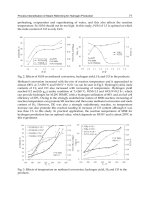
1992)
Mechanical Testing:
Patterned
samples, nominally
(8 x 8)
mm
2
, were interlocked
by
applying
a
load
to the
upper
substrate;
the
insertion pressure
is
monitored
by
placing
the
entire assembly
on an
electronic
force
scale.
The
bond strength
of the
mating structures
is
then
characterised
by
direct measurements
of the
tensile load needed
to
induce failure. Bond strength
is
determined
by
applying
a
tensile
load
through
a
pulley
and
measuring
the
force
necessary
for
separation. Separation
of the
samples
(failure)
is
always accompanied
by
damaged
areas
only
on
some regions
of the
mating surfaces, implying that
the
samples
are
only
interlocked over these damaged regions.
The
fraction
of the
damaged area
is
found
to
be
proportional
to the
insertion pressure (Figure 5.4(a)). Also,
the
tensile load necessary
to
induce failure
is
proportional
to the
fraction
of the
damaged
area
(Figure 5.4(b)).
Extrapolation
of the
straight line plot
of the
area damaged against
the
tensile strength
to 100
percent interlocking yields
a
tensile strength
of
approximately
1.0
MPa.
Failure Analysis:
The
analysis assumes
a
simple cantilever model
as
shown
in
Figure 5.5.
In
the
figure,
F
n
is the
interaction force between
the
tabs
and / is the
length
of the
tab.
The
bending
stress,
a, is
given
by
a(x)
=
M(x)y
(5.2)
where
x is
measured
from
the
edge
of the tab
that
is
attached
to the
substrate,
the
bending
moment M(x)
is
given
by
F
n
(l
- x) I
z
is the
moment
of
inertia (bh
3
/12)
of
the
rectangular cross-sectional area
of
width
b and
thickness
h
about
the
centroidal axis
(z-axis),
and y is the
distance
from
the
neutral plane.
The
maximum bending stress
a
max
occurs
when
x = 0 and y =
±h/2
and is
given
by
6/y
bh
2
(5.3)
122
SILICON MICROMACHINING: BULK
t t t t t t t t
I
I I I I I I I
Figure
5.5
Simple cantilever model
of the
failure
mode
of
silicon microvelcro (Han
et al.
1992)
Similarly,
the
maximum shearing stress r
max
occurs
at the
neutral plane
>' = 0:
3F
n
(5.4)
a
max
is
higher than
T
max
with
the
ratio
of
T
max
/a
max
equal
to
h/4l
for the
design
used.
Visual
examination
of the
tested samples indicates that
failure
is
accompanied
by
damage
to the
edge
of the tab and is
consistent
with
the
failure
occurring when
a
max
exceeds
the
yield point a
yp
. From Figure 5.5,
we
have
_ ext -
r
n — . .
\-J-J)
4
sm
a
where
F
ext
is the
tensile load (i.e. force
per
unit
surface area) applied
to the
sample.
Using Equation
(5.3),
we get
"
max
— • , , i . "• * exi —
2bh
2
sma
which, when
we
include friction with
a
static coefficient
/z,
becomes
2a
mM
bh
2
sin
a
ext
~
3d
2
l(\
+
Mcota)
The
tensile strength (failure load)
of the
structure
can be
found
by
substituting design
values
for b, h, l, a, and /z
(0.5)
and by
substituting
a
yp
(6 x 10
5
kPa for the
oxide)
for
a
max
in
Equation (5.7)
to
obtain
a
value
of
F
ext
equal
to 1.1
MPa, which
is in
agreement
with
the
value obtained
from
the
extrapolation
of
data
in
Figure
5.4(b).
This
finding
confirms
that
the
failure mechanism
is
that
of
bending
stress,
which
exceeds
the
oxide
yield point
at the tab
edge.
ISOTROPIC
AND
ORIENTATION-DEPENDENT
WET
ETCHING
123
Worked
Example
E5.2: Undoped Silicon Cantilever Beams
Objective:
To
fabricate
a
cantilever beam oriented
in the
(100) direction
on
(100) silicon wafers
(Choit
and
Smits 1993).
Process
Flow:
1.
A
layer
of
SiO
2
that
is 0.5 um
thick
is
grown
on a
(100) n-type silicon wafer.
The
wafer
is
spin-coated with
a
layer
of
positive photoresist.
The
masks needed
to
fabricate
the
cantilevers
are
shown
in
Figure
5.6(a,
b).
Cross-hatched areas represent
opaque regions
of the
masks.
For
mask
1
(Figure
5.6
(a)),
w
1
=
2(w
b
+
and
(5.8)
where
l
b
, w
b
, and t
b
are the
length, width,
and
thickness
of the
beam, respectively.
l
1
and
w
1
are
shown
in
Figure 5.6(a).
For
mask
2
(Figure 5.6(b)),
we
have
= w
b
+
and
l
2
=
(5.9)
where
d is a
small parameter that corrects design errors
and
mask misalignment,
l
2
and
w
2
are
shown
in
Figure 5.6(b).
The two
masks have essentially
the
same pattern,
except that mask
2 has a
smaller beam width than mask
1. The
wafer
is
patterned
with
mask
1. The
wafer
is
oriented
in
such
a way
that
the
length
of the
cantilever
beam
is in the
(010) direction
of the
wafer,
as
shown
in
Figure 5.6(c).
2. The
wafer
is
then immersed
in a
bath
of
buffered
oxide etch (BOE)
to
remove
the
SiO
2
in the
areas
that
are not
covered
by
photoresist,
and
this
is
followed
by
dissolving
the
resist
in an
acetone bath.
A
transverse cross section
of the
beam region
after
the
resist
has
been removed
is
shown
in
Figure 5.7(a).
The
wafer
is now
ready
to be
bulk-etched
in
sodium hydroxide (NaOH)
at 55 °C.
3.
Etching will take place
in
regions where
the
(100) planes
of
silicon
are
exposed.
Lateral etching
of
silicon directly underneath
the
SiO
2
passivation layer will also
occur;
the
lateral planes that
are
etched
are the
(100) equivalent planes. These planes
are
normal
to the
substrates.
The
rate
of
downward etching
is the
same
as
that
of
lateral etching; this
will
result
in
walls
that
are
almost completely vertical (see
Figure 5.7(b)). Planes
are
formed
at the
clamped
end of the
cantilever beam
(111).
Mask
1
IT
JL
Mask
2
H
h
W-)
(a) (b)
Figure
5.6
Masks required
to
fabricate
the
cantilever
(100)
Si
wafer
(c)
124
SILICON
MICROMACHINING:
BULK
H—M
dw
b
d
•H
H K-
w,
'b+V2
d w
b
d
K H
/
Hh*-HK
(a)
(d)
Figure
5.7
Four
process
steps
to
make
and
release
the
cantilever
4. The
wafer
is
then
etched
in BOE to
remove
all the
SiO
2
and is
then
cleaned
and
oxidised
to
grow
a
fresh
layer
of
SiO
2
that
is 1 urn
thick.
The
wafer
is
spin-coated
with
a
layer
of
positive
photoresist
and
patterned
with
mask
2.
After
the
unprotected
oxide
is
etched
away
in
BOE,
the
resist
is
removed
in
acetone.
The
wafer
is
then
etched
in
NaOH
at 55 °C
until
the
bulk
silicon
is
completely
under-etched
in the
areas
that
are
directly
underneath
the
beam.
Figure
5.7(c,
d)
shows
the
evolution
of
the
silicon
cantilevers
etched
in
this
way at
different
stages
of the final
etching
in
NaOH.
5.3
ETCH-STOP
TECHNIQUES
Many
different
chemical etchants
for
silicon
are
known.
The
properties that make some
of
these etchants indispensable
to
micromachining
of
three-dimensional structures
are
selec-
tivity
and
directionality.
As
etching processes
in
polar solvents
are
fundamentally
charge
transport phenomena,
it is not
surprising that
the
etch-rate
may be
dopant-type-dependent,
dopant-concentration-dependent,
and
bias-dependent. Etch
processes
can be
made selec-
tive
by the use of
dopants
-
heavily doped regions etch more slowly
- or
even halted elec-
trochemically when observing
the
sudden
rise in
current through
an
etched
n-p
junction.
A
region where
wet (or
dry) etching tends
to
slow down
(or
halt)
is
called
an
etch-stop.
There
are
several ways
in
which
an
etch-stop region
can be
created.
In the
following
subsections,
two
such methods
by
which
etch-stops
are
created
are
discussed. These
methods are:
•
doping-selective etching (DSE)
•
bias-dependent etching
BSE
5.3.1 Doping-Selective Etching (DSE)
Silicon membranes
are
generally fabricated using
the
etch-stop phenomenon
of a
thin,
heavily boron-doped layer, which
can be
epitaxially grown
or
formed
by the
diffusion
or
implantation
of
boron into
a
lightly doped substrate. This stopping
effect
is a
general
property
of
basic
etching solutions such
as
KOH, NaOH, ethylenediamine pyrocatechol
ETCH-STOP
TECHNIQUES
125
(EDP),
and
hydrazine (see Table 5.2). Because
of the
heavy boron-doping,
the
lattice
constant
of
silicon decreases slightly, leading
to
highly strained membranes that
often
show slip planes. They are, however, taut
and
fairly rugged even
in a few
microns
of
thickness
and are
approximately
1 cm in
diameter.
The
technique
is not
suited
to
stress-
sensitive
microstructures that could lead
to the
movement
of the
structures without
an
external
load.
In
this case, other etch-stop methods should
be
employed.
Early
studies (Greenwood 1969; Bohg 1971)
on the
influence
of
boron doping
on the
etch rates
of EDP for
(100) silicon
at
room temperature have shown
a
constant etch rate
of
approximately
50
u,rn/h
for the
resistivity range between
0.1 and 200
Q-cm corresponding
to
boron concentration
from
2 ×
10
14
to 5 x
10
17
cm
–3
.
As the
boron concentration
is
raised
to
about
a
critical value
of 7 ×
10
19
cm
–3
,
corresponding
to a
resistivity
of
approx-
imately
0.002
£2-cm,
the
silicon remains
virtually
unattacked
by the
etching solution
(see
Table 5.2). Figure
5.8
shows
the
boron-doping etch-stop properties
for
both
KOH
and
EDP.
The
dependence
of the
etch rate
on the
dopant concentration
is
typically exploited
for
undercutting microstructures that
are
defined
by a
masked heavy boron
diffusion
Table
5.2
Dopant-dependent
etch
rates
of
selected
silicon
wet
etchants
Etchant
(Diluent)
EDP
(H
2
O)
KOH
(H
2
O)
NaOH (H
2
O)
Temperature
(°C)
115
85
65
(100)
Etch
rate
(um/min)
for
boron
doping
«;
10
19
cm
–3
0.75
1.4
0.25-1.0
Etch
rate
(urn/min)
for
boron-doping
~10
20
cm
–3
0.015
0.07
0.025-0.1
10
1
10
–1
KOH
concentration
•
10%
o 24%
A
42%
A
57%
10
17
10
18
10
19
Boron
concentration
(c
(a)
10
10
18
10
19
Boron
concentration
(cm
–3
)
(b)
Figure
5.8
Boron etch-stop
properties
for (a) KOH and (b) EDP
etchants
126
SILICON MICROMACHINING: BULK
in
a
lightly doped
n- or
p-type substrate.
If the
etch-stop
concentration threshold
lies
in
between
the
substrate
and
diffusion
concentrations,
the
p-substrate
(or n
-substrate
for
that
matter)
is
etched
out
from
underneath
the
high boron
diffusion.
A
silicon microstructure
with
a
geometry defined
by the
diffusion
mask
and a
thickness close
to the
diffusion
depth
is
hence
left
freely
suspended.
The
main benefits
of the
high boron etch-stop
are the
independence
of
crystal orien-
tation,
the
smooth surface
finish,
and the
possibilities
it
offers
for
fabricating released
structures
with arbitrary lateral geometry
in a
single etch step.
On the
other hand,
the
high
levels
of
boron required
are
known
to
introduce considerable mechanical
stress
into
the
material;
this
may
even cause buckling
or
even fracture
in a
diaphragm
or
other double-clamped structures. Moreover,
the
introduction
of
electrical
components
for
sensing purposes into these microstructures, such
as the
implantation
of
piezoresistors,
is
inhibited
by the
excessive
background doping.
The
latter consideration constitutes
an
important limitation
to the
applicability
of the
high boron dose etch-stop. Consequently,
bias-dependent BSE, commonly referred
to as an
electrochemical etch-stop,
is
currently
the
most widely used etch-stop technique.
5.3.2
Conventional
Bias-Dependent
BSE or
Electrochemical
Etch-Stop
In
electrochemical etching
of
silicon,
a
voltage
is
applied
to the
silicon
wafer
(anode),
a
counter
electrode (cathode)
in the
etching solution.
The
fundamental
steps
of the
etching
mechanism
are as
follows:
1.
Injection
of
holes into
the
semiconductor
to
raise
it to a
higher oxidation state
Si
+
2.
Attachment
of
negatively charged hydroxyl groups, OH
–
,
to the
positively charged
Si
3.
Reaction
of the
hydrated silicon with
the
complexing agent
in the
solution
4.
Dissolution
of the
reaction products into
the
etchant solution
In
bias-dependent etching, oxidation
is
promoted
by a
positive voltage applied
to the
silicon
wafer,
causing
an
accumulation
of
holes
at the
Si-solution
interface. Under these
conditions, oxidation
at the
surface proceeds rapidly while
the
oxide
is
readily dissolved
by
the
solution. Holes such
as H
+
ions
are
transported
to the
cathode
and
released there
as
hydrogen
gas
bubbles. Excess hole-electron pairs can,
in
addition,
be
created
at the
silicon
surface,
for
example,
by
optical excitation, thereby increasing
the
etch rate.
Figure
5.9
shows
an
electrochemical cell that
is
used
to
etch
Si in a 5
percent hydro-
fluoric
(HF) solution.
The
cathode plate used
is
made
of
platinum.
In the
etching situation
shown
in
Figure 5.9,
holes
are
injected into
the Si
electrode
and
they tend
to
reside
at
the Si
surface where they
oxidise
Si at the
surface
to
Si
+
.
The
oxidised silicon interacts
with
incoming
OH~
that
are
produced
by
dissociation
of
water
in the
solution
to
form
the
unstable Si(OH), which dissociates into SiO
2
and H
2
gas.
The
SiO
2
is
then dissolved
by
HF and
removed
from
the
silicon
surface.
The
current density-voltage characteristics
for
different
silicon types
and
resistivities
are
shown
in
Figure 5.10.
It is
apparent
from
Figure 5.10 that
the
current
density
is
very
much
dependent
on the
type
and the
resistivity (doping level)
of Si.
This dependence
on
the
type
and
resistivity
is the
property
that
is
utilised
in the
electrochemical etch-stop
phenomenon.
ETCH-STOP
TECHNIQUES
127
Figure
5.9
Electrochemical
cell
with
5
percent
HF
solution
to
etch
silicon.
The
voltage
V
a
applied
to
the
silicon
is
relative
to a
platinum reference electrode
.0Q.crn(p)
£
0.3 -
0.2
-
§
0.1 h
U
0.01
Q .cm (n)
0.3Q«cm(/i)
5 10
Voltage V
a
(v)
15
Figure
5.10 Plot
of
electrochemical current density against voltage
for
silicon doped
to
different
resistivities
To
understand
the
mechanisms
of
electrochemical
etch-stop,
it is
important
to
explore
in
more detail
the
current-voltage
(/- V)
characteristics
in
etching solutions that exhibit
strong
electrochemical etch-stop
effects.
The
curves
in
Figure 5.11
are
typically (I-V)
characteristics
for n- and
p-type
silicon
in
KOH.
We can
easily
see the
similarity
of
Figure 5.11
to the
well-known curve
of a
diode, except that
at a
certain voltage
the
current
suddenly
and
sharply drops.
Let us
define
the
open circuit potential (OCP)
as the
potential
at
which
the
current
/ is
zero,
and the
passivating potential (PP)
as the
potential
at
which
the
current suddenly drops
from
its
maximum value.
The two
regions
of
interest
are
the
ones separated
by the PP.
Only cathodic
to the PP is the
sample etched, whereas
just
anodic
to it, an
oxide grows
and the
surface
is
passivated.
The
insulating oxide layer
that
is
formed during
the
etching process brings about
the
drastic
fall
in
current
at the
PP. The
difference between this etch
and the HF
etch
described
in
Figure
5.9 is the
fact
that
in the
latter etch
the
oxide
is
dissolved
by the HF
solution, whereas
in the
former
etch
the
oxide
is not
readily dissolved
in the KOH
solution. Another important
feature
of
Figure 5.11
is the
different behaviour
of the two
dopant types. When applying
a
voltage
between
the two
passivating potentials
of n- and
p-type,
one
expects,
in
accordance
with
the
characteristics shown
in
Figure 5.11, that only
the
p-type sample,
and not the
n-type sample, would
be
etched. This
is the
doping-selective
effect
that
is
used
as an
etch-stop.