VHDL Programming by Example phần 9 pdf
Bạn đang xem bản rút gọn của tài liệu. Xem và tải ngay bản đầy đủ của tài liệu tại đây (436.88 KB, 50 trang )
■ Accurate timing check support
—
Checks include setup checks, hold
checks, pulsewidth checks, period checks, and accurate glitch
detection.
■ Many ways to specify functionality
—
Functionality can be specified
with truth tables, state tables, boolean primitives, or a behavioral
description.
All of these features give the designer the ability to create timing-
accurate FPGA or ASIC libraries.
VITAL Simulation Process
Overview
The place and route tool generates a number of output files, as we saw in
the last chapter. The VITAL simulation uses two of these files. The first
is the VHDL netlist. This is a file containing component declarations, sig-
nals, and component instantiations that connect all of the components
together with the declared signals to form the functionality of the design.
This file is read by the VITAL simulator and used to create the compo-
nent connectivity in the database.
The second file is an SDF (Standard Delay Format) file that describes the
timing for the design. For each instance in the netlist, this file contains SDF
statements that describe the delays and timing checks for the instance. This
information is used during simulation to model the timing behavior.
To build the VITAL simulation database, the simulator needs to have
a VITAL library that contains components for the target technology and
the VHDL netlist and SDF timing file from the place and route tools. The
simulator uses the netlist to instantiate the proper instances from the
VITAL library in the internal database and then apply timing to the
instances with the SDF file. Each of the instances contains a number of
generics that receive the timing information. The timing data is used
within the model to provide the correct behavior of the underlying device.
VITAL Implementation
VITAL descriptions follow a standard style and make use of standard
functions and procedures from two VITAL packages. The VITAL Timing
Chapter Seventeen
382
Package contains procedures and functions for accurate delay modeling,
timing checks, and timing error reporting. The VITAL Primitives Package
contains built-in primitives that are optimized for simulator performance.
Most VITAL-compliant simulators build the primitives package into the
simulator for optimum performance.
VITAL contains two styles of modeling that can be back-annotated with
SDF timing data for timing-accurate simulation. The first style, VITAL
level 1, uses only VITAL primitives for modeling the behavior of the
design. The second, VITAL level 0, has the capability to back-annotate
timing, but uses behavioral statements to describe the functionality of the
design. VITAL level 1 descriptions can be accelerated by VITAL-compliant
simulators because the constructs used are built into the simulator. VITAL
level 0 descriptions may not be accelerated because these descriptions use
behavioral constructs which may not be built in.
Simple VITAL Model
To understand how the VITAL modeling process works, a simple VITAL
model is examined. The model describes the behavior of a 2-input AND
gate. The symbol for the AND gate is shown in Figure 17-3.
The AND gate has two inputs, in1 and in2, and an output y. When
modeled with VITAL, this device has an input delay on inputs in1 and
383
CPU:Vital Simulation
in1 Input Delay
Output Delay
int2 -> y
in1
y
in2
Figure 17-3
VITAL AND Gate.
in2, and pin-to-pin delays from input in1 to output y and from input in2
to output y.
Following is the VITAL model that implements the functionality of the
AND2 device:
CELL AND2
library IEEE;
use IEEE.STD_LOGIC_1164.all;
use IEEE.VITAL_Timing.all;
library alt_vtl;
use alt_vtl.SUPPORT.all;
entity declaration
entity AND2 is
generic(
TimingChecksOn: Boolean := True;
XGenerationOn: Boolean := False;
InstancePath: STRING := “*”;
tpd_IN1_Y : VitalDelayType01 := DefPropDelay01;
tpd_IN2_Y : VitalDelayType01 := DefPropDelay01;
tipd_IN1 : VitalDelayType01 := DefPropDelay01;
tipd_IN2 : VitalDelayType01 := DefPropDelay01);
port(
Y : out STD_LOGIC;
IN1 : in STD_LOGIC;
IN2 : in STD_LOGIC);
attribute VITAL_LEVEL0 of AND2 : entity is TRUE;
end AND2;
architecture body
architecture AltVITAL of AND2 is
attribute VITAL_LEVEL1 of AltVITAL : architecture is
TRUE;
SIGNAL IN1_ipd : STD_ULOGIC := ‘U’;
SIGNAL IN2_ipd : STD_ULOGIC := ‘U’;
begin
INPUT PATH DELAYs
WireDelay : block
begin
VitalWireDelay (IN1_ipd, IN1, tipd_IN1);
VitalWireDelay (IN2_ipd, IN2, tipd_IN2);
end block;
BEHAVIOR SECTION
VITALBehavior : process (IN1_ipd, IN2_ipd)
Chapter Seventeen
384
functionality results
VARIABLE Results : STD_LOGIC_VECTOR(1 to 1) :=
VARIABLE Results : (others => ‘X’);
ALIAS Y_zd : STD_ULOGIC is Results(1);
output glitch detection variables
VARIABLE Y_GlitchData : VitalGlitchDataType;
begin
Functionality Section
Y_zd := (IN2_ipd) AND (IN1_ipd);
Path Delay Section
VitalPathDelay01 (
OutSignal => Y,
OutSignalName => “Y”,
OutTemp => Y_zd,
Paths => (0 => (IN1_ipd’last_event, tpd_IN1_Y,
Paths => (0 => (TRUE),
Paths => (1 => (IN2_ipd’last_event, tpd_IN2_Y,
Paths => (1 => (TRUE)),
GlitchData => Y_GlitchData,
Mode => DefGlitchMode,
XOn => DefGlitchXOn);
end process;
end AltVITAL;
configuration CFG_AND2_VITAL of AND2 is
for AltVITAL
end for;
end CFG_AND2_VITAL;
The model looks like standard VHDL with some different packages
included. In fact, the model is standard VHDL. The entity contains decla-
rations for the STD_1164 packages for the signal logic types, but also con-
tains USE clauses for the VITAL timing package. The VITAL timing pack-
age is needed in the entity for
AND2 to provide the type declarations for
the entity generics.
The entity statement contains four generics that are used to pass
delay information to the model. Each of the generics has a prefix that
represents the type of the delay. Generic tipd_in1 is an input delay for
input in1. Generic tipd_in2 is an input delay for input in2. Generic
385
CPU:Vital Simulation
tpd_in1_y models the pin-to-pin delay from input in1 to output y. Generic
tidp_in2_y models the pin-to-pin delay from input in2 to output y.
The timing information passed to these generics comes from the SDF
file generated by the place and route tool. Each of the delays passed to
the entity is instance specific.
Each of the generics has a type associated with it that represents how
many delay values can be held. In this example, the generic contains two
values. Delay
tr01 represents the delay value when the signal changes
from a
‘0’ to ‘1’ value. Delay tr10 represents the delay when the signal
changes from a
‘1’ to ‘0’ value.
The entity also contains other generics that control functionality of the
VITAL model. This example contains a generic called
TimingChecksOn
that controls whether or not the timing check functions in the VITAL
model are executed or not. Finally, the entity contains the input and
output ports for the model.
VITAL Architecture
The architecture for the VITAL model contains four distinct code areas.
These are the wire delay section, the timing violation section, the function
description section, and the path delay section. Not all models contain all
of these sections. Some models are purely combinational and do not need
timing check sections.
Wire Delay Section
The first section of the architecture is the wire delay section. The AND2
architecture starts with a number of library declarations; but notice that
the architecture also uses the VITAL primitives package. After the
architecture statement, the architecture declares two local signals,
in1_ipd and in2_ipd, and an attribute. The two signals are used to
delay the input signals to the entity. The delay values applied to the two
input signals represent the wiring delays to connect the physical gates
together. For instance, in Figure 17-4, gate U1 drives gates U2 and U3.
The wiring from gate U1 to gate U2 causes 8 nanoseconds of delay in
the path, but the wiring from U1 to U3 causes 10 nanoseconds of delay
in the path. With separate input delay values for each input, the wiring
delays can be modeled correctly.
Chapter Seventeen
386
Attribute VitalLevel1 specifies that the VITAL model is level 1
compliant. Level 1 models are modeled only with VITAL primitives and
can be accelerated. Some simulators have compliance checkers that can
validate level 1 compliance.
The architecture contains a block labeled WireDelay which contains
the VHDL description that actually delays the input signals. The block
contains a call to the VitalWireDelay procedure for each input port. The
VitalWireDelay procedure delays the input ports by the value passed to
the appropriate generic used in the procedure call. In this example,
generic tipd_in1 is used to delay input in1, and generic tipd_in2 is used
to delay input in2.
After the wire delay section is the timing check section. This example has
no timing check section because it is a purely combinational gate model.
The next section is the functionality section. This section contains the
statements that model the behavior of the device. This section starts with
a process labeled VitalBehavior. Notice that the process is sensitive to
the delayed versions of the two input signals, in1_ipd and in2_ipd. There
are a number of local variables declared and a statement that performs
an AND function of the two inputs. This AND function can be built into the
simulator so that execution can be accelerated.
The last section of the architecture starts with the VitalPathDelay
procedure call. This section is the path delay section. This section schedules
the new logic values calculated in the functionality section to occur after
the appropriate delay. This section consists of a VitalPathDelay01 proce-
dure call for each output from the entity.
387
CPU:Vital Simulation
U1
U2
U3
8 ns
8 ns
Figure 17-4
Wire Delay
Representation.
The VitalPathDelay01 procedure has a number of parameters passed
to it. These parameters are used to control what kind of glitch behavior
is wanted, the delays to be used, and the temporary data used to store sig-
nal information.
In this example, the
VitalPathDelay procedure is passed the following
parameters:
■
OutSignal
—
The signal to have the new value placed on it.
■
OutSignalName
—
The name of the output signal to be used in
glitch reporting or error reporting.
■
OutTemp
—
A temporary signal used to store the current value of
the signal for comparison.
■
Paths
—
An array used to store delay information. There is a table
entry for each delay arc through the device.
■ GlitchData
—
A temporary storage area used to store signal state
and transition information for use in calculating glitches.
■
Mode
—
Specifies the type of glitch behavior wanted.
■
GlitchKind
—
Specifies the kind of glitches generated, OnEvent or
OnDetect.
Flip-Flop Example
In this next section, we examine another VITAL model with more com-
plexity. This example shows the VITAL model for a DFF device. This
device has sequential behavior and needs to have timing checks to check
for illegal timing conditions:
CELL DFF
library IEEE;
use IEEE.STD_LOGIC_1164.all;
use IEEE.VITAL_Timing.all;
use IEEE.VITAL_Primitives.all;
library alt_vtl;
use alt_vtl.SUPPORT.all;
entity declaration
entity DFF is
generic(
TimingChecksOn: Boolean := True;
XGenerationOn: Boolean := False;
InstancePath: STRING := “*”;
Chapter Seventeen
388
tpd_PRN_Q_negedge : VitalDelayType01 :=
DefPropDelay01;
tpd_CLRN_Q_negedge : VitalDelayType01 :=
DefPropDelay01;
tpd_CLK_Q_posedge : VitalDelayType01 :=
DefPropDelay01;
tsetup_D_CLK_noedge_posedge : VitalDelayType :=
DefSetupHoldCnst;
tsetup_D_CLK_noedge_negedge : VitalDelayType :=
DefSetupHoldCnst;
thold_D_CLK_noedge_posedge : VitalDelayType :=
DefSetupHoldCnst;
thold_D_CLK_noedge_negedge : VitalDelayType :=
DefSetupHoldCnst;
tipd_D : VitalDelayType01 := DefPropDelay01;
tipd_CLRN : VitalDelayType01 := DefPropDelay01;
tipd_PRN : VitalDelayType01 := DefPropDelay01;
tipd_CLK : VitalDelayType01 := DefPropDelay01);
port(
Q : out STD_LOGIC;
D : in STD_LOGIC;
CLRN : in STD_LOGIC;
PRN : in STD_LOGIC;
CLK : in STD_LOGIC);
attribute VITAL_LEVEL0 of DFF : entity is TRUE;
end DFF;
architecture body
architecture AltVITAL of DFF is
attribute VITAL_LEVEL1 of AltVITAL : architecture is
TRUE;
SIGNAL D_ipd : STD_ULOGIC := ‘U’;
SIGNAL CLRN_ipd : STD_ULOGIC := ‘U’;
SIGNAL PRN_ipd : STD_ULOGIC := ‘U’;
SIGNAL CLK_ipd : STD_ULOGIC := ‘U’;
begin
INPUT PATH DELAYs
WireDelay : block
begin
VitalWireDelay (D_ipd, D, tipd_D);
VitalWireDelay (CLRN_ipd, CLRN, tipd_CLRN);
VitalWireDelay (PRN_ipd, PRN, tipd_PRN);
VitalWireDelay (CLK_ipd, CLK, tipd_CLK);
end block;
389
CPU:Vital Simulation
BEHAVIOR SECTION
VITALBehavior : process (D_ipd, CLRN_ipd, PRN_ipd,
CLK_ipd)
timing check results
VARIABLE Tviol_D_CLK : STD_ULOGIC := ‘0’;
VARIABLE TimingData_D_CLK : VitalTimingDataType :=
VitalTimingDataInit;
functionality results
VARIABLE Violation : STD_ULOGIC := ‘0’;
VARIABLE PrevData_Q : STD_LOGIC_VECTOR(1 to 6) ;
VARIABLE D_delayed : STD_ULOGIC := ‘U’;
VARIABLE CLK_delayed : STD_ULOGIC := ‘U’;
VARIABLE Results : STD_LOGIC_VECTOR(1 to 1) :=
(others => ‘X’);
output glitch detection variables
VARIABLE Q_VitalGlitchData : VitalGlitchDataType;
CONSTANT DFF_Q_tab : VitalStateTableType := (
Violation, CLRN_ipd, CLK_delayed, D_delayed, PRN_ipd,
CLK_ipd
( L, L, x, x, x, x, x, L ),
( L, H, L, H, x, H, x, H ),
( L, H, H, x, H, x, x, S ),
( L, H, x, x, L, x, x, H ),
( L, H, x, x, H, L, x, S ),
( L, x, L, L, H, H, x, L ) );
begin
Timing Check Section
if (TimingChecksOn) then
VitalSetupHoldCheck (
Violation => Tviol_D_CLK,
TimingData => TimingData_D_CLK,
TestSignal => D_ipd,
TestSignalName => “D”,
RefSignal => CLK_ipd,
RefSignalName => “CLK”,
SetupHigh => tsetup_D_CLK_noedge_
posedge,
SetupLow => tsetup_D_CLK_noedge_
posedge,
HoldHigh => thold_D_CLK_noedge_
posedge,
HoldLow => thold_D_CLK_noedge_
posedge,
Chapter Seventeen
390
CheckEnabled => TO_X01(( (NOT PRN_ipd)
) OR ( (NOT
CLRN_ipd) ) ) /= ‘1’,
RefTransition => ‘/’,
HeaderMsg => InstancePath & “/DFF”,
XOn => DefTimingXon,
MsgOn => DefTimingMsgon );
end if;
Functionality Section
Violation := Tviol_D_CLK;
VitalStateTable(
StateTable => DFF_Q_tab,
DataIn => (
Violation, CLRN_ipd, CLK_delayed,
D_delayed, PRN_ipd, CLK_ipd),
Result => Results,
NumStates => 1,
PreviousDataIn => PrevData_Q);
D_delayed := D_ipd;
CLK_delayed := CLK_ipd;
Path Delay Section
VitalPathDelay01 (
OutSignal => Q,
OutSignalName => “Q”,
OutTemp => Results(1),
Paths => (0 => (PRN_ipd’last_event,
tpd_PRN_Q_negedge, TRUE),
1 => (CLRN_ipd’last_event,
tpd_CLRN_Q_negedge, TRUE),
2 => (CLK_ipd’last_event,
tpd_CLK_Q_posedge, TRUE),
3 => (D_ipd’last_event,
tpd_CLK_Q_posedge, TRUE)),
GlitchData => Q_VitalGlitchData,
Mode => DefGlitchMode,
XOn => DefGlitchXOn);
end process;
end AltVITAL;
configuration CFG_DFF_VITAL of DFF is
for AltVITAL
end for;
end CFG_DFF_VITAL;
391
CPU:Vital Simulation
The first thing to notice about this model is that there are quite a few
more generics used to pass timing information to the model. This is
because this model has more input ports; therefore, there are more input
delay generics and the model contains timing checks that need timing
information passed to them.
The wire delay section now delays four input ports instead of two. The
D,
CLRN, PRN, and CLK inputs are delayed in the wire delay section. The archi-
tecture for the DFF also contains a number of local signals and variables used
to hold intermediate values for the timing check and functionality sections.
The final declaration item in the architecture declaration section is a table
that is used to model the behavior of the
DFF. This DFF model uses a VITAL
State Table procedure to model the behavior of the device. This table is used
in the functionality section of the model by the VitalStateTable procedure
call. The signal values of the signals passed to the VitalStateTable proce-
dure call are compared to the values in the table, and the new values for the
output signals and next state are predicted.
The timing check section for this example contains a VitalSetupHold-
Check
procedure call. This procedure checks the setup and hold of data
changes versus the clock for the DFF device. The violation signal returned
by the
VitalSetupHoldCheck procedure is used to affect the behavior of
the DFF device by the fact that its value is passed to the
VitalStateTable
that controls the behavior of the DFF device.
The functionality section of the DFF device contains the single call to the
VitalStateTable procedure to calculate the value of the Q output based on
the values of the input ports, the previous state, and the violation signal
from the timing check procedures. Based on all of these inputs, a table row
matches, and the new Q output is passed to the path delay section.
The path delay section looks very similar to the path delay section for
the AND2 device discussed previously. The path delay section contains a
single call to the
VitalPathDelay01 procedure, which schedules output Q
with the appropriate delay value.
To see how all of these VITAL functions and procedures are imple-
mented, look at the VITAL packages included on the CD with the book or
visit www.vhdl.org/vital.
SDF File
The other piece of functionality needed to complete the VITAL simulation
picture is the SDF back-annotation file. This file is generated by the place
Chapter Seventeen
392
and route tools and contains accurate timing for the device. The SDF file
contains timing information for all of the generics in the VITAL library
that need data passed to them. Following is a sample SDF file:
(DELAYFILE
(SDFVERSION “2.1”)
(DESIGN “cpu”)
(DATE “10/25/97 10:59:58”)
(VENDOR “Altera”)
(PROGRAM “MAX+plus II”)
(VERSION “Version 7.2 RC2 2/14/97”)
(DIVIDER .)
(VOLTAGE :5:) (PROCESS “typical”) (TEMPERATURE :25:)
(TIMESCALE 100ps)
(CELL
(CELLTYPE “DFF”)
(INSTANCE DFF_457)
(DELAY
(ABSOLUTE
(IOPATH (posedge CLK) Q (32:32:32) (32:32:32)))
(ABSOLUTE
(IOPATH (negedge PRN) Q (36:36:36) (36:36:36)))
(ABSOLUTE
(IOPATH (negedge CLRN) Q (37:37:37) (37:37:37)))
)
(TIMINGCHECK
(SETUP D (posedge CLK) (2:2:2))
(HOLD D (posedge CLK) (10:10:10))
))
)
The SDF file starts with a header section that describes the name of
the design the file will back-annotate, the vendor that generated the file, the
environment used to generate the timing numbers, and so on. After the
header, the file consists of a number of cells. Each cell in the SDF file rep-
resents an instance in the VHDL netlist produced by the place and route
tools. Each cell contains the type of cell, the instance name in the netlist,
and timing information to be back-annotated to the design. The VITAL-
compliant simulator reads the SDF file and matches the generics in the
VHDL source with the delay constructs in the SDF file. For instance, an
IOPATH construct in the SDF file specifies the rising and falling delays from
and input to an output signal. The IOPATH construct is converted into
generic names and values to be applied to the VITAL simulation. The de-
signer of the VITAL model must ensure that the names used in the SDF
model and the names of the generics used in the VITAL model match so
that the generics can be properly matched with proper timing values.
393
CPU:Vital Simulation
The last section is a timing check section that contains timing infor-
mation for the timing checks of the cell, if they exist. The timing check
section of the SDF file is read by the VITAL simulator and extracts timing
information to plug into generics of the VITAL model. The timing check
generics control the timing values that are used in the timing checks of the
VITAL model while simulation is progressing.
The cell description in the preceding example is for the DFF model that
we looked at earlier. There are delay values for CLK to Q, PRN to Q, and CLRN
to Q, and values for the setup and hold check.
VITAL Simulation
To run the VITAL simulation, the designer first compiles the VITAL li-
brary into a simulator library. The device manufacturers supply VITAL
libraries for their devices. Next, the VITAL netlist is compiled to the
working library, and, finally, the SDF file is read in to back-annotate
the timing data into the design. After these steps have been completed,
the designer runs the VITAL simulation in the same manner as the RTL
simulation that we ran earlier.
The first step is to compile the VITAL library into a simulator library
so that it can be referenced. It is best if this library is compiled into the
location specified by the netlist from the place and route tool so that no
manual code modification is necessary. The following shows the first few
lines of the VITAL netlist generated by the MaxPlusII place and route
tool. The complete netlist is on the CD. Notice that the VITAL netlist
expects the VITAL component declarations, package VCOMPONENTS, to be
located in a library named alt_vtl:
MAX+plus II Version 7.2 RC2 2/14/97
Sat Oct 25 10:59:34 1997
LIBRARY IEEE;
USE IEEE.std_logic_1164.all;
LIBRARY alt_vtl;
USE alt_vtl.VCOMPONENTS.all;
ENTITY cpu IS
PORT (
addr : OUT std_logic_vector(15 downto 0);
data : INOUT std_logic_vector(15 downto 0);
clock : IN std_logic;
Chapter Seventeen
394
ready : IN std_logic;
reset : IN std_logic;
rw : OUT std_logic;
vma : OUT std_logic);
END cpu;
ARCHITECTURE EPF10K10TC144_a3 OF cpu IS
SIGNAL gnd : std_logic := ‘0’;
SIGNAL vcc : std_logic := ‘1’;
SIGNAL ……
……….
To compile the VCOMPONENTS package into library alt_vtl, the follow-
ing commands are executed in ModelSim:
vlib alt_vtl
vcom -work alt_vtl alt_vtl.cmp
Because there are no other library declarations for the actual vital
library, the vital library entities need to be compiled into the working
library to be visible. Following is the command to perform this step:
vcom alt_vtl.vhd
After these two files have been compiled, the VITAL netlist can be com-
piled into the working library. The following command compiles the
netlist:
vcom cpuout.vhd
We still need to simulate design TOP to verify the gate-level imple-
mentation of the CPU. However, this time, the CPU RTL description is re-
placed with a VITAL description of the CPU. This can be accomplished
by two different methods. The first involves compilation order, and the
second is by direct specification. Remember that the last architecture
compiled is used by default for an entity. By compiling architecture
EPF10K10TC144_a3 last, this architecture is used for entity cpu.
The other method is to write a configuration for architecture top that
specifies exactly which architecture is to be used. The following example
shows two configuration statements for the two different implementations
of the CPU:
configuration topconrtl of top is
for behave
for U1 : cpu use entity work.cpu(behave);
end for;
395
CPU:Vital Simulation
end for;
end topconrtl;
configuration topconstruct of top is
for behave
for U1 : cpu use entity work.cpu(EPF10K10TC144_a3);
end for;
end for;
end topconstruct;
Configuration topconrtl specifies the rtl implementation configuration
for entity top, and configuration topconstruct specifies the structural
implementation. Notice that the structural architecture was named the
same as the device that was implemented by the place and route tools.
To complete the simulation setup process, the final compilations
needed are shown here:
vcom top.vhd
vcom topconstruct.vhd
After these steps, the design is ready for simulation. To load the design
into the simulator, the following command is executed:
vsim topconstruct
The simulator brings up its windows and begins the simulation. If the
simulation is run ahead 500 nanoseconds, we can see the CPU start the
reset sequence as instructions are fetched. This is shown in Figure 17-5.
Chapter Seventeen
396
Figure 17-5
The Simulator
Window.
Running the simulation through the entire process verifies the func-
tionality of the placed and routed design. To verify the timing and
functionality, we need to back-annotate the timing from place and route
to the simulation.
Back-Annotated Simulation
To run timing back-annotated simulation, we don’t need to recompile. We
only need to specify to the simulator which SDF file to read. This is done
by the following command:
vsim -sdfmax /u1=cpuout.sdf topconstruct
This command tells the simulator to back-annotate the VITAL simu-
lation of the CPU design with SDF file cpuout.sdf created by the place
and route tools. After this command has executed, the simulation is
invoked, and the SDF file is back-annotated to component U1 (cpu) and
simulation started. Running the simulation produces the waveform shown
in Figure 17-6.
The back-annotated delays are seen on the waveforms for addr and
data around time 400 nanoseconds. Notice that, instead of one transition,
the waveforms have a number of transitions that finally settle out. Using
this timing information, the designer can now increase the clock speed
397
CPU:Vital Simulation
Figure 17-6
Simulation
Waveform.
until the design stops working to determine the maximum speed that
the design will run. By running the design through the entire simulation,
the functionality and timing of the design can be verified for correctness.
When the design meets the functionality and timing requirements, the
design can be signed off and built.
SUMMARY
In this chapter, we examined VITAL simulation and how to perform
VITAL simulation on the CPU design. The rest of the book contains use-
ful appendices that describe some of the standard types, functions, and
procedures used throughout the book.
Chapter Seventeen
398
CHAPTER
18
At Speed
Debugging
Techniques
Throughout the book so far we have discussed a number
of techniques for implementing VHDL designs and ways
to make sure that the VHDL designs behave as expected.
These techniques include simulation, synthesis of the
design to an FPGA or ASIC, and gate-level simulation
using VITAL libraries. A new technique called At-Speed
Debugging is just becoming available that allows much
higher performance verification than a typical simulator,
yet provides the design visibility necessary to properly
debug a design. This technique provides designers with
the ability to debug their design in the target system, at
target speed, at the VHDL RTL level.
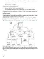
Figure 18-1 shows a block diagram of how this works.
The VHDL for the device is read into a tool that auto-
matically creates and inserts a small debug core into the
device that probes internal signals. The debug core is cre-
ated based on information from the designer about what
18
signals are to be probed. This debug core communicates through the
JTAG port on the device to an HDL debugger executing on a host plat-
form. The HDL debugger sends and receives data from the debug core
and displays this data in context with the HDL for the design. Wave-
forms of the internal device data can also be displayed, providing the
ability to trace down problems in the design.
This technique works well for any design, but it works especially well
for designs where a tremendous amount of data must be processed by
the device to determine whether the device is working properly. For
instance, devices that process audio or video information require a
tremendous amount of data to be processed before it can be determined
that the device is working properly. A video processor might need to pro-
duce several minutes of high-quality video data to determine whether
the encryption decoding algorithm is working properly. Running at or
near speed will allow images to be generated quickly and the device
function to be analyzed for correctness.
The only system as of this writing that performs as described is the
Bridges2Silicon debugger from Bridges2Silicon. A block diagram of the
system is shown in Figure 18-2.
The Bridges2Silicon debugger contains two tools. The Bridges2Silicon
instrumentor reads the VHDL description and adds the debug core, called
an Intelligent In-Circuit Emulator (IICE) to the design. The Bridges2Silicon
debugger communicates with the JTAG port on the target device, reads
the database created by the instrumentor, and reads the original source
files created by the designer.
Chapter Eighteen
400
FPGA or
SOC
FPGA or
SOC
IICE
JTAG
Hardware System
HDL
Debugger
Figure 18-1
At-Speed Debugging
Overview.
Instrumentor
The designer reads the VHDL design into the instrumentor and specifies
which signals to probe and which breakpoints to enable. The instrumentor
generates a new VHDL description of the design with the IICE core added
and connected to the appropriate places in the design. Once the new VHDL
description has been created, the designer synthesizes, and place and route
the new VHDL description. In an FPGA design environment, the device is
programmed with the new device file created by place and route.
Debugger
Once the board is powered up, and the FPGA device is programmed with
the new device file from place and route, the debugger can communicate
with the device through the JTAG port. The debugger also reads the data-
base file created by the Instrumentor and the original VHDL source files.
The instrumentor database relates the real signals on the device to the
location of the signals in the original HDL.
Debug CPU Design
Let’s now look at the process of debugging the CPU design using the
Bridges2Silicon Debugger. The first step is to create a project containing
all of the HDL files for the design.
401
At Speed Debugging Techniques
HDL
Sources
IICE
Implement
(Synthesis, P&R)
SOC
Implement
(Synthesis, P&R)
Bridges2Silicon
Instrumentor
Instrumented
HDL
Sources
B2S
Project
Bridges2Silicon
Instrumentor
B2S
Project
Bridges2Silicon
Debugger
JTAG
Bridges2Silicon
Debugger
JTAG
Figure 18-2
Bridges2Silicon
Debugger Overview.
Create Project
To create a project, use the project editor invoked from the File
menu or from the toolbar. The Project Editor window is shown in Fig-
ure 18-3.
To add to the project, use the file navigator in the upper left to nav-
igate to the location of files. First select the files and use the right arrow
key to add the files to the Design File list on the right of the project
editor window as shown in Figure 18-4. Now the design source files
need to be re-ordered so that the files are read in the proper order,
which is specified by the order of the list. The package
cpulib.vhd
needs to be read first so that it is available to all the other design files.
The easiest way to move
cpulib.vhd to the top of the list is to select
and drag it to the top of the list. The other file that needs to be moved
is the top level of the design, cpu.vhd. File cpu.vhd needs to be moved to
the bottom of the list so that it is the last file read.
Chapter Eighteen
402
Figure 18-3
Bridges2Silicon Project
Editor Window.
403
At Speed Debugging Techniques
Specify Top-Level Parameters
Once all the files have been specified, the parameters for the top level
need to be specified so that the design elements can be properly linked.
There are two parameters that need to be specified: the TOP-LEVEL UNIT
and TOP-LEVEL LANGUAGE. TOP-LEVEL UNIT specifies which design unit is
the top level and will be linked. This value will be specified as CPU. TOP-
LEVEL LANGUAGE
specifies the default language used to compile the design
and to write out the instrumented design.
TOP-LEVEL LANGUAGE is specified
as VHDL by clicking the VHDL radio button. This is shown in Figure 18-5.
Now that we have specified all the needed parameters, click the OK but-
ton, which saves the project and also compiles the project. After compila-
tion, Figure 18-6 shows the design loaded into the Instrumentor Window.
Specify Project Parameters
Once all the files have been added to the project, the device parame-
ters need to be specified. These parameters determine how the device
Figure 18-4
Files added to Project
File List.
will communicate with the JTAG port and the debugger on the host
platform. Use the dialog box shown in Figure 18-7 to set up the device
and IICE configuration settings.
1.
Device family. We use the Altera Apex technology.
2. JTAG port. The choices are
b2s and builtin. We will choose builtin
so that we can use JTAG communication with the JTAG tap controller
already present in the Altera device. This choice is used predominately
and
b2s is only used when the board containing the device is not connected
to the JTAG chain on the board.
3.
Type of RAM. This parameter specifies the type of RAM to be used for
the sample buffer that stores internal signal data. The choices are block-
ram, logic, and behavioral. This example will use blockram, the most com-
mon selection and the most efficient. This selection will build the sample
buffer from blockrams available on the FPGA device. If the logic choice is
selected, the sample buffer will be built from flip-flops in user logic. This
choice is used when there is limited blockram available and is not as effi-
cient as blockram. The third choice is behavioral and will generate a
behavioral model for the sample buffer. This choice will let the synthesis
tool choose the sample buffer implementation based on available resources.
4.
Sample clock. This parameter specifies a signal that will be used to
clock the data into the sample buffer. This signal can be any signal in the
design but must be a clocklike signal. For instance, this signal should be
the output of a register so that it does not contain glitches. In this example
the signal
/clk will be used.
5. Sample depth. This parameter specifies how many samples are gath-
ered when a trigger occurs. Depending on how much data are required
to find a bug, this value can be any power of 2 that will fit into the Buffer
Type specified for the device. In this example, the value 256 will be used.
Instrument Signals
Now that the design has been compiled and the communication parameters
specified, the signals to be instrumented can be selected. For this example
we are going to debug the control block. All breakpoints and signals in the
control block for the reset sequence will be instrumented for use later dur-
ing debugging. The debugger GUI shows only the signals and breakpoints
that can be instrumented. Clicking the Radio button next to a signal or
breakpoint will instrument that signal or breakpoint. Figure 18-8 shows the
Radio buttons for the reset sequence selected for sampling and debugging.
Chapter Eighteen
404
Write Instrumented Design
Once all the signals and breakpoints have been instrumented, the instru-
mented design can be written out. This design will include the original
design tree plus the IICE core added for debugging. The IICE core will be
connected in such a way as to probe all the instrumented signals in the
design. Select the File Save and Instrument menu items to write out the
instrumented design.
Implement New Design
The write instrumented design process will produce a new version of the
VHDL files for the CPU design. These files need to be synthesized as
described in earlier chapters. The output of the synthesis process is an
EDIF netlist. The EDIF netlist is placed and routed with the Altera
Quartus tools to produce a file that is programmed into the Altera device
405
At Speed Debugging Techniques
Figure 18-5
Top Level Unit and
Language Specified.
as described earlier. Finally the new programming file is programmed
into the Altera device with the Altera programming software.
Start Debug
Now that the device has been programmed with the new netlist, the device
can be debugged with the Bridges2Silicon debugger. The debugger is
invoked, and the project created by the Bridges2Silicon instrumentor
is loaded into the debugger. This project loads the original source files for
the project into the debugger. The debugger now shows only instrumented
signals and breakpoints.
Enable Breakpoint
To enable a breakpoint, click on the radio button next to it. To put a watch
expression on a signal, click the signal and specify a signal expression value.
Chapter Eighteen
406
Figure 18-6
Compiled Project with
Debug Items Shown.