rfid handbook fundamentals and applications in contactless smart cards and identification second edition phần 2 docx
Bạn đang xem bản rút gọn của tài liệu. Xem và tải ngay bản đầy đủ của tài liệu tại đây (2.47 MB, 52 trang )
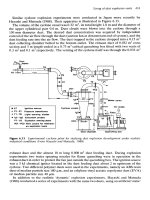
Figure 3.12: Representation of full duplex, half duplex and sequential
systems over time. Data transfer from the reader to the transponder is
termed downlink, while data transfer from the transponder to the reader
is termed uplink
Unfortunately, the literature relating to RFID has not yet been able to agree a
consistent nomenclature for these system variants. Rather, there has been a
confusing and inconsistent classification of individual systems into full and half
duplex procedures. Thus pulsed systems are often termed half duplex systems
— this is correct from the point of view of data transfer — and all unpulsed
systems are falsely classified as full duplex systems. For this reason, in this
book pulsed systems — for differentiation from other procedures, and unlike
most RFID literature(!) — are termed sequential systems (SEQ).
3.2.1 Inductive coupling
3.2.1.1 Power supply to passive transponders
An inductively coupled transponder comprises an electronic data-carrying
device, usually a single microchip, and a large area coil that functions as an
antenna.
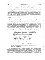
Inductively coupled transponders are almost always operated passively. This
means that all the energy needed for the operation of the microchip has to be
provided by the reader (Figure 3.13). For this purpose, the reader's antenna
coil generates a strong, high frequency electromagnetic field, which penetrates
the cross-section of the coil area and the area around the coil. Because the
wavelength of the frequency range used (<135 kHz: 2400 m, 13.56 MHz: 22.1
m) is several times greater than the distance between the reader's antenna and
the transponder, the electromagnetic field may be treated as a simple magnetic
alternating field with regard to the distance between transponder and antenna
(see Section 4.2.1.1 for further details).
Figure 3.13: Power supply to an inductively coupled transponder from
the energy of the magnetic alternating field generated by the reader
A small part of the emitted field penetrates the antenna coil of the transponder,
which is some distance away from the coil of the reader. A voltage U
i
is
generated in the transponder's antenna coil by inductance. This voltage is
rectified and serves as the power supply for the data-carrying device
(microchip). A capacitor C
r
is connected in parallel with the reader's antenna
coil, the capacitance of this capacitor being selected such that it works with the
coil inductance of the antenna coil to form a parallel resonant circuit with a
This document was created by an unregistered ChmMagic, please go to to register it. Thanks.
resonant frequency that corresponds with the transmission frequency of the
reader. Very high currents are generated in the antenna coil of the reader by
resonance step-up in the parallel resonant circuit, which can be used to
generate the required field strengths for the operation of the remote
transponder.
The antenna coil of the transponder and the capacitor C
1
form a resonant
circuit tuned to the transmission frequency of the reader. The voltage U at the
transponder coil reaches a maximum due to resonance step-up in the parallel
resonant circuit.
The layout of the two coils can also be interpreted as a transformer
(transformer coupling), in which case there is only a very weak coupling
between the two windings (Figure 3.14). The efficiency of power transfer
between the antenna coil of the reader and the transponder is proportional to
the operating frequency f, the number of windings n, the area A enclosed by
the transponder coil, the angle of the two coils relative to each other and the
distance between the two coils.
Figure 3.14: Different designs of inductively coupled transponders. The
photo shows half finished transponders, i.e. transponders before
injection into a plastic housing (reproduced by permission of AmaTech
GmbH & Co. KG, D-Pfronten)
As frequency f increases, the required coil inductance of the transponder coil,
and thus the number of windings n decreases (135 kHz: typical 100–1000
windings, 13.56 MHz: typical 3–10 windings). Because the voltage induced in
the transponder is still proportional to frequency f (see Chapter 4), the reduced
number of windings barely affects the efficiency of power transfer at higher
frequencies. Figure 3.15 shows a reader for an inductively coupled
transponder.
This document was created by an unregistered ChmMagic, please go to to register it. Thanks.
Figure 3.15: Reader for inductively coupled transponder in the
frequency range <135 kHz with integral antenna (reproduced by
permission of easy-key System, micron, Halbergmoos)
3.2.1.2 Data transfer transponder → reader
Load modulation
As described above, inductively coupled systems are based upon a
transformer-type coupling between the primary coil in the reader and the
secondary coil in the transponder. This is true when the distance between the
coils does not exceed 0.16 λ, so that the transponder is located in the near
field of the transmitter antenna (for a more detailed definition of the near and
far fields, please refer to Chapter 4).
If a resonant transponder (i.e. a transponder with a self-resonant frequency
corresponding with the transmission frequency of the reader) is placed within
the magnetic alternating field of the reader's antenna, the transponder draws
energy from the magnetic field. The resulting feedback of the transponder on
the reader's antenna can be represented as transformed impedance Z
T
in the
antenna coil of the reader. Switching a load resistor on and off at the
transponder's antenna therefore brings about a change in the impedance Z
T
,
and thus voltage changes at the reader's antenna (see Section 4.1.10.3). This
has the effect of an amplitude modulation of the voltage U
L
at the reader's
antenna coil by the remote transponder. If the timing with which the load
resistor is switched on and off is controlled by data, this data can be transferred
from the transponder to the reader. This type of data transfer is called load
modulation.
This document was created by an unregistered ChmMagic, please go to to register it. Thanks.
Table 3.6: Overview of the power consumption of various RFID-ASIC building blocks (Atmel,
1994). The minimum supply voltage required for the operation of the microchip is 1.8 V, the
maximum permissible voltage is 10 V
Memory
(Bytes)
Write/read
distance
Power
consumption
FrequencyApplication
ASIC#1615 cm
10 µA
120 kHzAnimal ID
ASIC#23213 cm
600 µA
120 kHzGoods
flow,
access
check
ASIC#32562 cm
6 µA
128 kHzPublic
transport
ASIC#42560.5 cm<1 mA
4 MHz
[*]
Goods
flow, public
transport
ASIC#5256<2 cm~1 mA4/13.56
MHz
Goods flow
ASIC#6256100 cm
500 µA
125 kHzAccess
check
ASIC#720480.3 cm<10 mA4.91
MHz
[*]
Contactless
chip cards
ASIC#8102410 cm~1 mA13.56 MHzPublic
transport
ASIC#98100 cm<1 mA125 kHzGoods flow
ASIC#10128100 cm<1 mA125 kHzAccess
check
[*]
Close coupling system.
To reclaim the data at the reader, the voltage tapped at the reader's antenna is
rectified. This represents the demodulation of an amplitude modulated signal.
An example circuit is shown in Section 11.3.
Load modulation with subcarrier
Due to the weak coupling between the reader antenna and the transponder
antenna, the voltage fluctuations at the antenna of the reader that represent the
useful signal are smaller by orders of magnitude than the output voltage of the
reader.
In practice, for a 13.56 MHz system, given an antenna voltage of approximately
100 V (voltage step-up by resonance) a useful signal of around 10 mV can be
expected (=80 dB signal/noise ratio). Because detecting this slight voltage
change requires highly complicated circuitry, the modulation sidebands created
by the amplitude modulation of the antenna voltage are utilised (Figure 3.16).
This document was created by an unregistered ChmMagic, please go to to register it. Thanks.
Figure 3.16: Generation of load modulation in the transponder by
switching the drain-source resistance of an FET on the chip. The
reader illustrated is designed for the detection of a subcarrier
If the additional load resistor in the transponder is switched on and off at a very
high elementary frequency f
S
, then two spectral lines are created at a distance
of ± f
S
around the transmission frequency of the reader f
READER
, and these
can be easily detected (however f
S
must be less than f
READER
). In the
terminology of radio technology the new elementary frequency is called a
subcarrier). Data transfer is by ASK, FSK or PSK modulation of the subcarrier
in time with the data flow. This represents an amplitude modulation of the
subcarrier.
Load modulation with a subcarrier creates two modulation sidebands at the
reader's antenna at the distance of the subcarrier frequency around the
operating frequency f
READER
(Figure 3.17). These modulation sidebands can
be separated from the significantly stronger signal of the reader by bandpass
(BP) filtering on one of the two frequencies f
READER
± f
S
. Once it has been
amplified, the subcarrier signal is now very simple to demodulate.
Figure 3.17: Load modulation creates two sidebands at a distance of
the subcarrier frequency f
S
around the transmission frequency of the
reader. The actual information is carried in the sidebands of the two
subcarrier sidebands, which are themselves created by the modulation
of the subcarrier
Because of the large bandwidth required for the transmission of a subcarrier,
this procedure can only be used in the ISM frequency ranges for which this is
permitted, 6.78 MHz, 13.56 MHz and 27.125 MHz (see also Chapter 5).
This document was created by an unregistered ChmMagic, please go to to register it. Thanks.
Example circuit-load modulation with subcarrier
Figure 3.18 shows an example circuit for a transponder using load modulation
with a subcarrier. The circuit is designed for an operating frequency of 13.56
MHz and generates a subcarrier of 212 kHz.
Figure 3.18: Example circuit for the generation of load modulation with
subcarrier in an inductively coupled transponder
The voltage induced at the antenna coil L1 by the magnetic alternating field of
the reader is rectified using the bridge rectifier (D1–D4) and after additional
smoothing (C1) is available to the circuit as supply voltage. The parallel
regulator (ZD 5V6) prevents the supply voltage from being subject to an
uncontrolled increase when the transponder approaches the reader antenna.
Part of the high frequency antenna voltage (13.56 MHz) travels to the
frequency divider's timing input (CLK) via the protective resistor (R1) and
provides the transponder with the basis for the generation of an internal
clocking signal. After division by 2
6
(= 64) a subcarrier clocking signal of 212
kHz is available at output Q7. The sub-carrier clocking signal, controlled by a
serial data flow at the data input (DATA), is passed to the switch (T1). If there is
a logical HIGH signal at the data input (DATA), then the subcarrier clocking
signal is passed to the switch (T1). The load resistor (R2) is then switched on
and off in time with the subcarrier frequency.
Optionally in the depicted circuit the transponder resonant circuit can be
brought into resonance with the capacitor C1 at 13.56 MHz. The range of this
'minimal transponder' can be significantly increased in this manner.
Subharmonic procedure
The subharmonic of a sinusoidal voltage A with a defined frequency f
A
is a
sinusoidal voltage B, whose frequency f
B
is derived from an integer division of
the frequency f
A
. The subharmonics of the frequency f
A
are therefore the
frequencies f
A
/2, f
A
/3, f
A
/4
In the subharmonic transfer procedure, a second frequency f
B
, which is usually
lower by a factor of two, is derived by digital division by two of the reader's
transmission frequency f
A
. The output signal f
B
of a binary divider can now be
modulated with the data stream from the transponder. The modulated signal is
then fed back into the transponder's antenna via an output driver.
This document was created by an unregistered ChmMagic, please go to to register it. Thanks.
One popular operating frequency for subharmonic systems is 128 kHz. This
gives rise to a transponder response frequency of 64 kHz.
The transponder's antenna consists of a coil with a central tap, whereby the
power supply is taken from one end. The transponder's return signal is fed into
the coil's second connection (Figure 3.19).
Figure 3.19: Basic circuit of a transponder with subharmonic back
frequency. The received clocking signal is split into two, the data is
modulated and fed into the transponder coil via a tap
3.2.2 Electromagnetic backscatter coupling
3.2.2.1 Power supply to the transponder
RFID systems in which the gap between reader and transponder is greater
than 1 m are called long-range systems. These systems are operated at the
UHF frequencies of 868 MHz (Europe) and 915 MHz (USA), and at the
microwave frequencies 2.5 GHz and 5.8 GHz. The short wavelengths of these
frequency ranges facilitate the construction of antennas with far smaller
dimensions and greater efficiency than would be possible using frequency
ranges below 30 MHz.
In order to be able to assess the energy available for the operation of a
transponder we first calculate the free space path loss a
F
in relation to the
distance r between the transponder and the reader's antenna, the gain G
T
and
G
R
of the transponder's and reader's antenna, plus the transmission frequency
f of the reader:
(3.1)
The free space path loss is a measure of the relationship between the HF
power emitted by a reader into 'free space' and the HF power received by the
transponder.
Using current low power semiconductor technology, transponder chips can be
produced with a power consumption of no more than 5 µW (Friedrich and
Annala, 2001). The efficiency of an integrated rectifier can be assumed to be
5–25% in the UHF and microwave range (Tanneberger, 1995). Given an
efficiency of 10%, we thus require received power of P
e
= 50 µW at the terminal
of the transponder antenna for the operation of the transponder chip. This
means that where the reader's transmission power is P
S
= 0.5 W EIRP
(effective isotropic radiated power) the free space path loss may not exceed 40
dB (P
s
/P
e
= 10 000/1) if sufficiently high power is to be obtained at the
transponder antenna for the operation of the transponder. A glance at Table
This document was created by an unregistered ChmMagic, please go to to register it. Thanks.
3.7 shows that at a transmission frequency of 868 MHz a range of a little over 3
m would be realisable; at 2.45 GHz a little over 1 m could be achieved. If the
transponder's chip had a greater power consumption the achievable range
would fall accordingly.
Table 3.7: Free space path loss a
F
at different frequencies and distances. The
gain of the transponder's antenna was assumed to be 1.64 (dipole), the gain
of the reader's antenna was assumed to be 1 (isotropic emitter)
Distance r868 MHz915 MHz2.45 GHz
0.3 m18.6 dB19.0 dB27.6 dB
1 m29.0 dB29.5 dB38.0 dB
3 m38.6 dB39.0 dB47.6 dB
10 m49.0 dB49.5 dB58.0 dB
In order to achieve long ranges of up to 15 m or to be able to operate
transponder chips with a greater power consumption at an acceptable range,
backscatter transponders often have a backup battery to supply power to the
transponder chip (Figure 3.20). To prevent this battery from being loaded
unnecessarily, the microchips generally have a power saving 'power down' or
'stand-by' mode. If the transponder moves out of range of a reader, then the
chip automatically switches over to the power saving 'power down' mode. In
this state the power consumption is a few µA at most. The chip is not
reactivated until a sufficiently strong signal is received in the read range of a
reader, whereupon it switches back to normal operation. However, the battery
of an active transponder never provides power for the transmission of data
between transponder and reader, but serves exclusively for the supply of the
microchip. Data transmission between transponder and reader relies
exclusively upon the power of the electromagnetic field emitted by the reader.
Figure 3.20: Active transponder for the frequency range 2.45 GHz. The
data carrier is supplied with power by two lithium batteries. The
This document was created by an unregistered ChmMagic, please go to to register it. Thanks.
transponder's microwave antenna is visible on the printed circuit board
in the form of a u-shaped area (reproduced by permission of Pepperl &
Fuchs, Mannheim)
3.2.2.2 Data transmission → reader
Modulated reflection cross-section
We know from the field of radar technology that electromagnetic waves are
reflected by objects with dimensions greater than around half the wavelength of
the wave. The efficiency with which an object reflects electromagnetic waves is
described by its reflection cross-section. Objects that are in resonance with the
wave front that hits them, as is the case for antennas at the appropriate
frequency, for example, have a particularly large reflection cross-section.
Power P
1
is emitted from the reader's antenna, a small proportion of which
(free space attenuation) reaches the transponder's antenna (Figure 3.21). The
power is supplied to the antenna connections as HF voltage and after
rectification by the diodes D
1
and D
2
this can be used as turn-on voltage for the
deactivation or activation of the power saving 'power down' mode. The diodes
used here are low barrier Schottky diodes, which have a particularly low
threshold voltage. The voltage obtained may also be sufficient to serve as a
power supply for short ranges.
Figure 3.21: Operating principle of a backscatter transponder. The
impedance of the chip is 'modulated' by switching the chip's FET
(Integrated Silicon Design, 1996)
A proportion of the incoming power is reflected by the antenna and
returned as power P
2
. The reflection characteristics (=reflection cross-section)
of the antenna can be influenced by altering the load connected to the antenna.
In order to transmit data from the transponder to the reader, a load resistor R
L
connected in parallel with the antenna is switched on and off in time with the
data stream to be transmitted. The amplitude of the power P
2
reflected from the
transponder can thus be modulated (→ modulated backscatter).
The power P
2
reflected from the transponder is radiated into free space. A
small proportion of this (free space attenuation) is picked up by the reader's
antenna. The reflected signal therefore travels into the antenna connection of
the reader in the backwards direction and can be decoupled using a directional
coupler and transferred to the receiver input of a reader. The forward signal of
the transmitter, which is stronger by powers of ten, is to a large degree
suppressed by the directional coupler.
This document was created by an unregistered ChmMagic, please go to to register it. Thanks.
The ratio of power transmitted by the reader and power returning from the
transponder (P
1
/P
2
) can be estimated using the radar equation (for an
explanation, refer to Chapter 4).
3.2.3 Close coupling
3.2.3.1 Power supply to the transponder
Close coupling systems are designed for ranges between 0.1 cm and a
maximum of 1 cm. The transponder is therefore inserted into the reader or
placed onto a marked surface ('touch & go') for operation.
Inserting the transponder into the reader, or placing it on the reader, allows the
transponder coil to be precisely positioned in the air gap of a ring-shaped or
U-shaped core. The functional layout of the transponder coil and reader coil
corresponds with that of a transformer (Figure 3.22). The reader represents the
primary winding and the transponder coil represents the secondary winding of
a transformer. A high frequency alternating current in the primary winding
generates a high frequency magnetic field in the core and air gap of the
arrangement, which also flows through the transponder coil. This power is
rectified to provide a power supply to the chip.
Figure 3.22: Close coupling transponder in an insertion reader with
magnetic coupling coils
Because the voltage U induced in the transponder coil is proportional to the
frequency f of the exciting current, the frequency selected for power transfer
should be as high as possible. In practice, frequencies in the range 1–10 MHz
are used. In order to keep the losses in the transformer core low, a ferrite
material that is suitable for this frequency must be selected as the core
material.
Because, in contrast to inductively coupled or microwave systems, the
efficiency of power transfer from reader to transponder is very good, close
coupling systems are excellently suited for the operation of chips with a high
power consumption. This includes microprocessors, which still require some 10
mW power for operation (Sickert, 1994). For this reason, the close coupling
chip card systems on the market all contain microprocessors.
The mechanical and electrical parameters of contactless close coupling chip
cards are defined in their own standard, ISO 10536. For other designs the
This document was created by an unregistered ChmMagic, please go to to register it. Thanks.
operating parameters can be freely defined.
3.2.3.2 Data transfer transponder → reader
Magnetic coupling
Load modulation with subcarrier is also used for magnetically coupled data
transfer from the transponder to the reader in close coupling systems
.Subcarrier frequency and modulation is specified in ISO 10536 for close
coupling chip cards.
Capacitive coupling
Due to the short distance between the reader and transponder, close coupling
systems may also employ capacitive coupling for data transmission. Plate
capacitors are constructed from coupling surfaces isolated from one another,
and these are arranged in the transponder and reader such that when a
transponder is inserted they are exactly parallel to one another (Figure 3.23).
Figure 3.23: Capacitive coupling in close coupling systems occurs
between two parallel metal surfaces positioned a short distance apart
from each other
This procedure is also used in close coupling smart cards. The mechanical and
electrical characteristics of these cards are defined in ISO 10536.
3.2.4 Electrical coupling
3.2.4.1 Power supply of passive transponders
In electrically (i.e. capacitively) coupled systems the reader generates a strong,
high-frequency electrical field. The reader's antenna consists of a large,
electrically conductive area (electrode), generally a metal foil or a metal plate. If
a high-frequency voltage is applied to the electrode a high-frequency electric
field forms between the electrode and the earth potential (ground). The
voltages required for this, ranging between a few hundred volts and a few
thousand volts, are generated in the reader by voltage rise in a resonant circuit
made up of a coil L
1
in the reader, plus the parallel connection of an internal
capacitor C
1
and the capacitance active between the electrode and the earth
potential C
R-GND
. The resonant frequency of the resonant circuit corresponds
with the transmission frequency of the reader.
The antenna of the transponder is made up of two conductive surfaces lying in
a plane (electrodes). If the transponder is placed within the electrical field of the
reader, then an electric voltage arises between the two transponder electrodes,
This document was created by an unregistered ChmMagic, please go to to register it. Thanks.
which is used to supply power to the transponder chips (Figure 3.24).
Figure 3.24: An electrically coupled system uses electrical
(electrostatic) fields for the transmission of energy and data
Since a capacitor is active both between the transponder and the transmission
antenna (C
R-T
) and between the transponder antenna and the earth potential
(C
T-GND
) the equivalent circuit diagram for an electrical coupling can be
considered in a simplified form as a voltage divider with the elements C
R-T
, R
L
(input resistance of the transponder) and C
T-GND
(see Figure 3.26). Touching
one of the transponder's electrodes results in the capacitance C
T-GND
, and
thus also the read range, becoming significantly greater.
Figure 3.25: Necessary electrode voltage for the reading of a
This document was created by an unregistered ChmMagic, please go to to register it. Thanks.
transponder with the electrode size a × b = 4.5 cm × 7 cm (format
corresponds with a smart card), at a distance of 1 m (f = 125 kHz)
Figure 3.26: Equivalent circuit diagram of an electrically coupled RFID
system
The currents that flow in the electrode surfaces of the transponder are very
small. Therefore, no particular requirements are imposed upon the conductivity
of the electrode material. In addition to the normal metal surfaces (metal foil)
the electrodes can thus also be made of conductive colours (e.g. a silver
conductive paste) or a graphite coating (Motorola, Inc., 1999).
3.2.4.2 Data transfer transponder → reader
If an electrically coupled transponder is placed within the interrogation zone of
a reader, the input resistance R
L
of the transponder acts upon the resonant
circuit of the reader via the coupling capacitance C
R-T
active between the
reader and transponder electrodes, damping the resonant circuit slightly. This
damping can be switched between two values by switching a modulation
resistor R
mod
in the transponder on and off. Switching the modulation resistor
R
mod
on and off thereby generates an amplitude modulation of the voltage
present at L
1
and C
1
by the remote transponder. By switching the modulation
resistor R
mod
on and off in time with data, this data can be transmitted to the
reader. This procedure is called load modulation.
3.2.5 Data transfer reader → transponder
All known digital modulation procedures are used in data transfer from the
reader to the transponder in full and half duplex systems, irrespective of the
operating frequency or the coupling procedure. There are three basic
procedures:
ASK: amplitude shift keying
FSK: frequency shift keying
PSK: phase shift keying
Because of the simplicity of demodulation, the majority of systems use ASK
modulation.
This document was created by an unregistered ChmMagic, please go to to register it. Thanks.
3.3 Sequential Procedures
If the transmission of data and power from the reader to the data carrier alternates
with data transfer from the transponder to the reader, then we speak of a sequential
procedure (SEQ).
The characteristics used to differentiate between SEQ and other systems have
already been described in Section 3.2.
3.3.1 Inductive coupling
3.3.1.1 Power supply to the transponder
Sequential systems using inductive coupling are operated exclusively at frequencies
below 135 kHz. A transformer type coupling is created between the reader's coil and
the transponder's coil. The induced voltage generated in the transponder coil by the
effect of an alternating field from the reader is rectified and can be used as a power
supply.
In order to achieve higher efficiency of data transfer, the transponder frequency must
be precisely matched to that of the reader, and the quality of the transponder coil must
be carefully specified. For this reason the transponder contains an on-chip trimming
capacitor to compensate for resonant frequency manufacturing tolerances.
However, unlike full and half duplex systems, in sequential systems the reader's
transmitter does not operate on a continuous basis. The energy transferred to the
transmitter during the transmission operation charges up a charging capacitor to
provide an energy store. The transponder chip is switched over to stand-by or power
saving mode during the charging operation, so that almost all of the energy received
is used to charge up the charging capacitor. After a fixed charging period the reader's
transmitter is switched off again.
The energy stored in the transponder is used to send a reply to the reader. The
minimum capacitance of the charging capacitor can be calculated from the necessary
operating voltage and the chip's power consumption:
(3.2)
where V
max
, V
min
are limit values for operating voltage that may not be exceeded, I is
the power consumption of the chip during operation and t is the time required for the
transmission of data from transponder to reader.
For example, the parameters I = 5 µA, t = 20 ms, V
max
= 4.5 V and V
min
= 3.5 V yield a
charging capacitor of C = 100 nF (Schürmann, 1993).
3.3.1.2 A comparison between FDX/HDX and SEQ systems
Figure 3.27 illustrates the different conditions arising from full/half duplex (FDX/HDX)
and sequential (SEQ) systems.
This document was created by an unregistered ChmMagic, please go to to register it. Thanks.
Figure 3.27: Comparison of induced transponder voltage in FDX/HDX and
SEQ systems (Schürmann, 1993)
Because the power supply from the reader to the transponder in full duplex systems
occurs at the same time as data transfer in both directions, the chip is permanently in
operating mode. Power matching between the transponder antenna (current source)
and the chip (current consumer) is desirable to utilise the transmitted energy
optimally. However, if precise power matching is used only half of the source voltage
(=open circuit voltage of the coil) is available. The only option for increasing the
available operating voltage is to increase the impedance (=load resistance) of the
chip. However, this is the same as decreasing the power consumption.
Therefore the design of full duplex systems is always a compromise between power
matching (maximum power consumption P
chip
at U
chip
= 1/2U
O
) and voltage matching
(minimum power consumption P
chip
at maximum voltage U
chip
= U
O
).
The situation is completely different in sequential systems: during the charging
process the chip is in stand-by or power saving mode, which means that almost no
power is drawn through the chip.
The charging capacitor is fully discharged at the beginning of the charging process
and therefore represents a very low ohmic load for the voltage source (Figure 3.27:
start loading). In this state, the maximum amount of current flows into the charging
capacitor, whereas the voltage approaches zero (=current matching). As the charging
capacitor is charged, the charging current starts to decrease according to an
exponential function, and reaches zero when the capacitor is fully charged. The state
of the charged capacitor corresponds with voltage matching at the transponder coil.
This achieves the following advantages for the chip power supply compared to a
full/half duplex system:
The full source voltage of the transponder coil is available for the
operation of the chip. Thus the available operating voltage is up to
twice that of a comparable full/half duplex system.
The energy available to the chip is determined only by the
capacitance of the charging capacitor and the charging period. Both
values can in theory (!) be given any required magnitude. In
full/half duplex systems the maximum power consumption of the
chip is fixed by the power matching point (i.e. by the coil geometry
and field strength H).
3.3.1.3 Data transmission transponder → reader
In sequential systems (Figure 3.28) a full read cycle consists of two phases, the
charging phase and the reading phase (Figure 3.29).
This document was created by an unregistered ChmMagic, please go to to register it. Thanks.
Figure 3.28: Block diagram of a sequential transponder by Texas Instruments
TIRIS® Systems, using inductive coupling
Figure 3.29: Voltage path of the charging capacitor of an inductively coupled
SEQ transponder during operation
The end of the charging phase is detected by an end of burst detector, which
monitors the path of voltage at the transponder coil and thus recognises the moment
when the reader field is switched off. At the end of the charging phase an on-chip
oscillator, which uses the resonant circuit formed by the transponder coil as a
frequency determining component, is activated. A weak magnetic alternating field is
generated by the transponder coil, and this can be received by the reader. This gives
an improved signal-interference distance of typically 20 dB compared to full/half
duplex systems, which has a positive effect upon the ranges that can be achieved
using sequential systems.
The transmission frequency of the transponder corresponds with the resonant
frequency of the transponder coil, which was adjusted to the transmission frequency
of the reader when it was generated.
In order to be able to modulate the HF signal generated in the absence of a power
supply, an additional modulation capacitor is connected in parallel with the resonant
circuit in time with the data flow. The resulting frequency shift keying provides a 2 FSK
modulation.
After all the data has been transmitted, the discharge mode is activated to fully
discharge the charging capacitor. This guarantees a safe Power-On-Reset at the start
of the next charging cycle.
3.3.2 Surface acoustic wave transponder
Surface acoustic wave (SAW) devices are based upon the piezoelectric effect and on
the surface-related dispersion of elastic (=acoustic) waves at low speed. If an (ionic)
crystal is elastically deformed in a certain direction, surface charges occur, giving rise
to electric voltages in the crystal (application: piezo lighter). Conversely, the
application of a surface charge to a crystal leads to an elastic deformation in the
crystal grid (application: piezo buzzer). Surface acoustic wave devices are operated at
microwave frequencies, normally in the ISM range 2.45 GHz.
This document was created by an unregistered ChmMagic, please go to to register it. Thanks.
Electroacoustic transducers (interdigital transducers) and reflectors can be created
using planar electrode structures on piezoelectric substrates. The normal substrate
used for this application is lithium niobate or lithium tantalate. The electrode structure
is created by a photolithographic procedure, similar to the procedure used in
microelectronics for the manufacture of integrated circuits.
Figure 3.30 illustrates the basic layout of a surface wave transponder. A finger-shaped
electrode structure — the interdigital transducer — is positioned at the end of a long
piezoelectrical substrate, and a suitable dipole antenna for the operating frequency is
attached to its busbar. The interdigital transducer is used to convert between electrical
signals and acoustic surface waves.
Figure 3.30: Basic layout of an SAW transponder. Interdigital transducers and
reflectors are positioned on the piezoelectric crystal
An electrical impulse applied to the busbar causes a mechanical deformation to the
surface of the substrate due to the piezoelectrical effect between the electrodes
(fingers), which disperses in both directions in the form of a surface wave (rayleigh
wave). For a normal substrate the dispersion speed lies between 3000 and 4000 m/s.
Similarly, a surface wave entering the converter creates an electrical impulse at the
busbar of the interdigital transducer due to the piezoelectric effect.
Individual electrodes are positioned along the remaining length of the surface wave
transponder. The edges of the electrodes form a reflective strip and reflect a small
proportion of the incoming surface waves. Reflector strips are normally made of
aluminium; however some reflector strips are also in the form of etched grooves
(Meinke, 1992).
A high frequency scanning pulse generated by a reader is supplied from the dipole
antenna of the transponder into the interdigital transducer and is thus converted into
an acoustic surface wave, which flows through the substrate in the longitudinal
direction. The frequency of the surface wave corresponds with the carrier frequency of
the sampling pulse (e.g. 2.45 GHz) (Figure 3.31). The carrier frequency of the
reflected and returned pulse sequence thus corresponds with the transmission
frequency of the sampling pulse.
This document was created by an unregistered ChmMagic, please go to to register it. Thanks.
Figure 3.31: Surface acoustic wave transponder for the frequency range 2.45
GHz with antenna in the form of microstrip line. The piezocrystal itself is
located in an additional metal housing to protect it against environmental
influences (reproduced by permission of Siemens AG, ZT KM, Munich)
Part of the surface wave is reflected off each of the reflective strips that are distributed
across the substrate, while the remaining part of the surface wave continues to travel
to the end of the substrate and is absorbed there.
The reflected parts of the wave travel back to the interdigital transducer, where they
are converted into a high frequency pulse sequence and are emitted by the dipole
antenna. This pulse sequence can be received by the reader. The number of pulses
received corresponds with the number of reflective strips on the substrate. Likewise,
the delay between the individual pulses is proportional to the spatial distance between
the reflector strips on the substrate, and so the spatial layout of the reflector strips can
represent a binary sequence of digits.
Due to the slow dispersion speed of the surface waves on the substrate the first
response pulse is only received by the reader after a dead time of around 1.5 ms after
the transmission of the scanning pulse. This gives decisive advantages for the
reception of the pulse.
Reflections of the scanning pulse on the metal surfaces of the environment travel
back to the antenna of the reader at the speed of light. A reflection over a distance of
100 m to the reader would arrive at the reader 0.6 ms after emission from the reader's
antenna (travel time there and back, the signal is damped by > 160 dB). Therefore,
when the transponder signal returns after 1.5 ms all reflections from the environment
of the reader have long since died away, so they cannot lead to errors in the pulse
sequence (Dziggel, 1997).
The data storage capacity and data transfer speed of a surface wave transponder
depend upon the size of the substrate and the realisable minimum distance between
the reflector strips on the substrate. In practice, around 16–32 bits are transferred at a
data transfer rate of 500 kbit/s (Siemens, n.d.).
The range of a surface wave system depends mainly upon the transmission power of
the scanning pulse and can be estimated using the radar equation (Chapter 4). At the
permissible transmission power in the 2.45 GHz ISM frequency range a range of 1–2
m can be expected.
This document was created by an unregistered ChmMagic, please go to to register it. Thanks.
Chapter 4: Physical Principles of RFID
Systems
Overview
The vast majority of RFID systems operate according to the principle of
inductive coupling. Therefore, understanding of the procedures of power and
data transfer requires a thorough grounding in the physical principles of
magnetic phenomena. This chapter therefore contains a particularly intensive
study of the theory of magnetic fields from the point of view of RFID.
Electromagnetic fields — radio waves in the classic sense — are used in RFID
systems that operate at above 30 MHz. To aid understanding of these systems
we will investigate the propagation of waves in the far field and the principles of
radar technology.
Electric fields play a secondary role and are only exploited for capacitive data
transmission in close coupling systems. Therefore, this type of field will not be
discussed further.
This document was created by an unregistered ChmMagic, please go to to register it. Thanks.
4.1 Magnetic Field
4.1.1 Magnetic field strength H
Every moving charge (electrons in wires or in a vacuum), i.e. flow of current, is
associated with a magnetic field (Figure 4.1). The intensity of the magnetic field can be
demonstrated experimentally by the forces acting on a magnetic needle (compass) or
a second electric current. The magnitude of the magnetic field is described by the
magnetic field strength H regardless of the material properties of the space.
Figure 4.1: Lines of magnetic flux are generated around every current-carrying
conductor
In the general form we can say that: 'the contour integral of magnetic field strength
along a closed curve is equal to the sum of the current strengths of the currents within
it' (Kuchling, 1985).
(4.1)
We can use this formula to calculate the field strength H for different types of
conductor. See Figure 4.2.
Figure 4.2: Lines of magnetic flux around a current-carrying conductor and a
current-carrying cylindrical coil
This document was created by an unregistered ChmMagic, please go to to register it. Thanks.
Table 4.1: Constants used
ConstantSymbolValue and unit
Electric field constant
ε
08.85 × 10
-12
As/Vm
Magnetic field constant
µ
01.257 × 10
-6
Vs/Am
Speed of lightc299792 km/s
Boltzmann constantk
1.380662 × 10
-23
J/K
In a straight conductor the field strength H along a circular flux line at a distance r is
constant. The following is true (Kuchling, 1985):
(4.2)
4.1.1.1 Path of field strength H(x) in conductor loops
So-called 'short cylindrical coils' or conductor loops are used as magnetic antennas to
generate the magnetic alternating field in the write/read devices of inductively coupled
RFID systems (Figure 4.3).
Figure 4.3: The path of the lines of magnetic flux around a short cylindrical
coil, or conductor loop, similar to those employed in the transmitter antennas
of inductively coupled RFID systems
This document was created by an unregistered ChmMagic, please go to to register it. Thanks.
Table 4.2: Units and abbreviations used
VariableSymbolUnitAbbreviation
Magnetic field strengthHAmpere per meterA/m
Magnetic flux (n =
number of windings)
Φ
Volt secondsVs
Ψ = nΦ
Magnetic inductanceBVolt seconds per
meter squared
Vs/m
2
InductanceLHenryH
Mutual inductanceMHenryH
Electric field strengthEVolts per metreV/m
Electric currentIAmpereA
Electric voltageUVoltV
CapacitanceCFaradF
FrequencyfHertzHz
Angular frequency
ω = 2πf
1/seconds1/s
LengthlMetrem
AreaAMetre squared
m
2
SpeedvMetres per secondm/s
ImpedanceZOhm
O
Wavelength
λ
Metrem
PowerPWattW
Power densitySWatts per metre
squared
W/m
2
If the measuring point is moved away from the centre of the coil along the coil axis (x
axis), then the strength of the field H will decrease as the distance x is increased. A
more in-depth investigation shows that the field strength in relation to the radius (or
area) of the coil remains constant up to a certain distance and then falls rapidly (see
Figure 4.4). In free space, the decay of field strength is approximately 60 dB per
decade in the near field of the coil, and flattens out to 20 dB per decade in the far
field of the electromagnetic wave that is generated (a more precise explanation of
these effects can be found in Section 4.2.1).
This document was created by an unregistered ChmMagic, please go to to register it. Thanks.
Figure 4.4: Path of magnetic field strength H in the near field of short cylinder
coils, or conductor coils, as the distance in the x direction is increased
The following equation can be used to calculate the path of field strength along the x
axis of a round coil (= conductor loop) similar to those employed in the transmitter
antennas of inductively coupled RFID systems (Paul, 1993):
(4.3)
where N is the number of windings, R is the circle radius r and x is the distance from
the centre of the coil in the x direction. The following boundary condition applies to this
equation: d << R and x < λ/2π (the transition into the electromagnetic far field begins at
a distance >2π; see Section 4.2.1).
At distance 0 or, in other words, at the centre of the antenna, the formula can be
simplified to (Kuchling, 1985):
(4.4)
We can calculate the field strength path of a rectangular conductor loop with edge
length a × b at a distance of x using the following equation. This format is often used
as a transmitter antenna.
(4.5)
Figure 4.4 shows the calculated field strength path H(x) for three different antennas at
a distance 0–20 m. The number of windings and the antenna current are constant in
each case; the antennas differ only in radius R. The calculation is based upon the
following values: H1: R = 55 cm, H2: R = 7.5 cm, H3: R = 1 cm.
The calculation results confirm that the increase in field strength flattens out at short
This document was created by an unregistered ChmMagic, please go to to register it. Thanks.
distances (x < R) from the antenna coil. Interestingly, the smallest antenna exhibits a
significantly higher field strength at the centre of the antenna (distance = 0), but at
greater distances (x > R) the largest antenna generates a significantly higher field
strength. It is vital that this effect is taken into account in the design of antennas for
inductively coupled RFID systems.
4.1.1.2 Optimal antenna diameter
If the radius R of the transmitter antenna is varied at a constant distance x from the
transmitter antenna under the simplifying assumption of constant coil current I in the
transmitter antenna, then field strength H is found to be at its highest at a certain ratio
of distance x to antenna radius R. This means that for every read range of an RFID
system there is an optimal antenna radius R. This is quickly illustrated by a glance at
Figure 4.4: if the selected antenna radius is too great, the field strength is too low even
at a distance x = 0 from the transmission antenna. If, on the other hand, the selected
antenna radius is too small, then we find ourselves within the range in which the field
strength falls in proportion to x
3
.
Figure 4.5 shows the graph of field strength H as the coil radius R is varied. The
optimal coil radius for different read ranges is always the maximum point of the graph
H(R). To find the mathematical relationship between the maximum field strength H
and the coil radius R we must first find the inflection point of the function H(R) (see
equation 4.3) (Lee, 1999). To do this we find the first derivative H'(R) by differentiating
H(R) with respect to R:
(4.6)
Figure 4.5: Field strength H of a transmission antenna given a constant
distance x and variable radius R, where I = 1 A and N = 1
The inflection point, and thus the maximum value of the function H(R), is found from
the following zero points of the derivative H'(R):
(4.7)
The optimal radius of a transmission antenna is thus twice the maximum desired read
range. The second zero point is negative merely because the magnetic field H of a
This document was created by an unregistered ChmMagic, please go to to register it. Thanks.
conductor loop propagates in both directions of the x axis (see also Figure 4.3).
However, an accurate assessment of a system's maximum read range requires
knowledge of the interrogation field strength H
min
of the transponder in question (see
Section 4.1.9). If the selected antenna radius is too great, then there is the danger that
the field strength H may be too low to supply the transponder with sufficient operating
energy, even at a distance x = 0.
4.1.2 Magnetic flux and magnetic flux density
The magnetic field of a (cylindrical) coil will exert a force on a magnetic needle. If a
soft iron core is inserted into a (cylindrical) coil — all other things remaining equal —
then the force acting on the magnetic needle will increase. The quotient I × N (Section
4.1.1) remains constant and therefore so does field strength. However, the flux density
— the total number of flux lines — which is decisive for the force generated (cf. Pauls,
1993), has increased.
The total number of lines of magnetic flux that pass through the inside of a cylindrical
coil, for example, is denoted by magnetic flux Φ. Magnetic flux density B is a further
variable related to area A (this variable is often referred to as 'magnetic inductance B
in the literature') (Reichel, 1980). Magnetic flux is expressed as:
(4.8)
The material relationship between flux density B and field strength H (Figure 4.6) is
expressed by the material equation:
(4.9)
Figure 4.6: Relationship between magnetic flux Φ and flux density B
The constant µ
0
is the magnetic field constant (µ
0
= 4π × 10
-6
Vs/Am) and describes
the permeability (= magnetic conductivity) of a vacuum. The variable µ
r
is called
relative permeability and indicates how much greater than or less than µ
0
the
permeability of a material is.
4.1.3 Inductance L
A magnetic field, and thus a magnetic flux Φ, will be generated around a conductor of
any shape. This will be particularly intense if the conductor is in the form of a loop
(coil). Normally, there is not one conduction loop, but N loops of the same area A,
through which the same current I flows. Each of the conduction loops contributes the
same proportion Φ to the total flux ψ (Paul, 1993).
(4.10)
This document was created by an unregistered ChmMagic, please go to to register it. Thanks.