designing with xilinx FPGAs using vivado
Bạn đang xem bản rút gọn của tài liệu. Xem và tải ngay bản đầy đủ của tài liệu tại đây (9.54 MB, 257 trang )
Sanjay Churiwala Editor
Designing
with Xilinx®
FPGAs
Using Vivado
Designing with Xilinx® FPGAs
Sanjay Churiwala
Editor
Designing with Xilinx®
FPGAs
Using Vivado
Editor
Sanjay Churiwala
Hyderabad, India
ISBN 978-3-319-42437-8
ISBN 978-3-319-42438-5
DOI 10.1007/978-3-319-42438-5
(eBook)
Library of Congress Control Number: 2016951983
© Springer International Publishing Switzerland 2017
This work is subject to copyright. All rights are reserved by the Publisher, whether the whole or part of
the material is concerned, specifically the rights of translation, reprinting, reuse of illustrations, recitation,
broadcasting, reproduction on microfilms or in any other physical way, and transmission or information
storage and retrieval, electronic adaptation, computer software, or by similar or dissimilar methodology
now known or hereafter developed.
The use of general descriptive names, registered names, trademarks, service marks, etc. in this publication
does not imply, even in the absence of a specific statement, that such names are exempt from the relevant
protective laws and regulations and therefore free for general use.
The publisher, the authors and the editors are safe to assume that the advice and information in this book
are believed to be true and accurate at the date of publication. Neither the publisher nor the authors or the
editors give a warranty, express or implied, with respect to the material contained herein or for any errors
or omissions that may have been made.
Printed on acid-free paper
This Springer imprint is published by Springer Nature
The registered company is Springer International Publishing AG Switzerland
Preface
The motivation for writing this book came as we saw that there are many books that
are published related to using Xilinx software for FPGA designs. Most of these
books are targeted to a specific version of Xilinx tools—be it ISE or Vivado or for a
specific device. Xilinx makes two major releases of Vivado each year. Each release
introduces significant new features and capabilities. Similarly, in each new device
architecture, Xilinx makes significant enhancements. Hence, books written on any
specific version of the software (or device architecture) get outdated very quickly.
Besides, Xilinx anyways publishes its own set of documents which are updated with
each major release of Vivado or FPGA architecture.
In this book, we have tried to concentrate on conceptual understanding of Vivado.
These are expected to remain current through the current architecture of the tool
chain. Our attempt has been that with a good conceptual understanding provided by
this book, you will be able to understand the details provided in the user guides,
which delve into the details of commands and options.
The Vivado software tool used for implementing a design on Xilinx’s FPGAs has
a lot of possible ways to read in a design. A user could describe the design in the
form of HDL or “C” or make use of Xilinx-provided IP or use a third-party IP or the
user could use his/her own HDL or “C” code as an IP to be used in multiple designs.
A user could also describe the design using still higher level of abstractions using IP
Integrator or SysGen. A design could also potentially use different types of inputs
(for different portions of the design). You can use this book to understand the inherent strengths of the various modes of design entry. You can then decide which
mechanism would be most suited for portions of the design. For the exact commands and syntax, you should refer to Xilinx documents. Our book provides a list
of reference materials. Depending on which specific capability you plan to use, you
can refer to the corresponding reference material.
Besides being useful to somebody who is new to Xilinx tools or FPGAs, the
book may be found useful for those users who are migrating from ISE to Vivado.
Vivado is conceptually very different from ISE. While ISE was mostly using proprietary formats for most of the flow, Vivado has moved on to industry standard
formats. Users who have been long-time ISE users sometimes find it difficult to get
v
vi
Preface
used to Vivado. This book helps them get a good understanding of Vivado concepts,
which should make it easier for them to transition to Vivado from ISE.
Though I’ve been involved in some of the user guides published by Xilinx, doing
this book in my personal capacity allows me to deviate from the official stand also,
wherever I wanted to, and share my real opinion.☺
The most effective way to make use of this book is to not worry about reading the
book from cover to cover. You can easily feel free to skip the chapters that deal with
topics which your design does not have.
Hyderabad, India
Sanjay Churiwala
Acknowledgments
I would like to express my gratitude to several of my colleagues and friends—
within Xilinx and outside—who agreed to write the chapters on their areas of expertise and also reviewed each other’s work. Each of these authors is highly
knowledgeable in their respective areas. They took time out of their regular work to
be able to contribute to this book.
I also thank my management chain at Xilinx, especially Arne Barras, Salil Raje,
Victor Peng, and Vamsi Boppana—who were supportive of this work, even though
this was being done in my personal capacity. I also thank the Xilinx legal/HR team,
who provided me with the necessary guidance, permissions, and approvals to be
able to complete this work, including usage of copyrighted material where relevant:
Rajesh Choudhary, Lorraine Cannon Lalor, David Parandoosh, Fred Hsu, Cynthia
Zamorski, and Silvia Gianelli. Amandeep Singh Talwar has been very helpful with
figures and various aspects of the word processor. I often reached out to him, whenever I was having difficulty on either of these two aspects. Shant Chandrakar and
Steve Trimberger helped me with specific items related to FPGA architecture. There
are many more who have been supporting this actively.
I also thank my many teachers, colleagues, and seniors who have been teaching
me so many things—that I could understand Semiconductor, EDA, and now specifically Xilinx FPGAs and Vivado. Over the last 23 years of professional experience in
this field, there are just too many of such people that I dare not even try to name some,
for the fear that I would end up filling up too many pages just with these names.
I also thank my family members. My immediate family members obviously
adjusted with the fact that instead of spending time with them, I was working on this
book. However, my entire extended family has been highly encouraging, by expressing their pride very openly at my past books.
vii
viii
Acknowledgments
And, I’m especially thankful to Charles Glaser of Springer, who is ever supportive of me working on any technical book. For this book, I also thank Murugesan
Tamilselvan of Springer who is working through the actual processes involved in
publication.
For me, writing continues to be a hobby that I cherish. And, once in a while,
when I encounter somebody who identifies me with one of my books, the fun just
gets multiplied many times for me. To anybody who has done this, I want to give a
big “thanks” for encouraging me.
Contents
1
State-of-the-Art Programmable Logic ..................................................
Brad Taylor
1
2
Vivado Design Tools ................................................................................
Sudipto Chakraborty
17
3
IP Flows ....................................................................................................
Cyrus Bazeghi
23
4
Gigabit Transceivers ...............................................................................
Vamsi Krishna
35
5
Memory Controllers ...............................................................................
Karthikeyan Palanisamy
49
6
Processor Options ...................................................................................
Siddharth Rele
65
7
Vivado IP Integrator ...............................................................................
Sagar Raghunandan Gosavi
75
8
SysGen for DSP .......................................................................................
Arvind Sundararajan
85
9
Synthesis...................................................................................................
Nithin Kumar Guggilla and Chaithanya Dudha
97
10
C-Based Design........................................................................................ 111
Duncan Mackay
11
Simulation ................................................................................................ 127
Saikat Bandopadhyay
12
Clocking ................................................................................................... 141
John Blaine
ix
x
Contents
13
Stacked Silicon Interconnect (SSI) ........................................................ 153
Brian Philofsky
14
Timing Closure ........................................................................................ 165
Srinivasan Dasasathyan
15
Power Analysis and Optimization ......................................................... 177
Anup Kumar Sultania, Chun Zhang, Darshak Kumarpal Gandhi,
and Fan Zhang
16
System Monitor ....................................................................................... 189
Sanjay Kulkarni
17
Hardware Debug ..................................................................................... 205
Brad Fross
18
Emulation Using FPGAs ........................................................................ 219
Paresh K. Joshi
19
Partial Reconfiguration and Hierarchical Design................................ 237
Amr Monawir
References ........................................................................................................ 251
Index ................................................................................................................. 255
Chapter 1
State-of-the-Art Programmable Logic
Brad Taylor
1.1
Introduction
The FPGA or field-programmable gate array is a wonderful technology used by
electronic system developers to design, debug, and implement unique hardware
solutions without having to develop custom silicon devices. Xilinx is a semiconductor manufacturer of standard FPGA chips which are sold blank or unprogrammed to
customers. The customers then program these devices to implement their unique
systems. If a feature changes or a bug is discovered, the user can simply load a new
program to the FPGA to create a new product or upgrade. This process can even
continue after shipment in the form of firmware upgrades. The act of programming
the FPGA is called configuration to distinguish it from loading any associated software programs. With modern FPGAs however, the line is blurring between hardware configuration and software programming.
All this programmability requires additional silicon area compared to hard ASIC
(application-specific integrated circuit) implementations of the same logic. This is
because in ASIC implementations the gates and wiring are fixed. This area cost penalty can be in the 1.5–10X range for FPGAs. However, the ASIC also must include the
development cost and schedule which can be in the range of $10–$500 million dollars
and can take several years with teams of hundreds of developers. With each generation
of lithography, the cost to develop an ASIC increases. For these reasons, most mediumsized and smaller systems rely on a mix of FPGAs for customization along with standard ASIC or ASSPs and memories.
This revolutionary technology has impacted the electronic product development
cycle for nearly all electronic devices since its introduction in the late 1980s.
B. Taylor (*)
Santa Cruz, California, USA
e-mail:
© Springer International Publishing Switzerland 2017
S. Churiwala (ed.), Designing with Xilinx® FPGAs,
DOI 10.1007/978-3-319-42438-5_1
1
2
1.2
B. Taylor
The Evolution of Programmable Logic
The initial user programmable devices called PLDs (programmable logic devices)
that were developed in 1978 by MMI could replace ten or so TTL gates and were
one time programmable. This led to the reprogrammable PLDs based on EEPROM
or EPROM technologies.
By 1985 advancing lithography enabled a new class of device, the FPGA. FPGAs
introduced two important new architecture features: programmable routing to interconnect the increasing number of gates on a device and a programmable gate called
a LUT or lookup table with an associated register. The initial devices from Xilinx
contained up to a hundred LUT and flip-flop pairs in a basic logic element called a
CLB or configurable logic block. Rather than using a permanently programmed
EPROM or EEPROM memory, Xilinx FPGAs relied on CMOS memories to hold
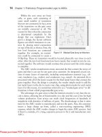
programming information. Figure 1.1 illustrates the technological improvement of
modern FPGAs relative to the original Xilinx XC2064 which had 64 programmable
logic cells.
The FPGA took its place as a central component in digital systems, replacing
PLDs and TTL for implementing glue logic. In the 1990s new uses began to emerge
for FPGAs, which were becoming more capable than just gluing I/O to processors.
The emerging Internet became a growth driver for FPGAs with FPGAs being used
for prototyping, initial deployment, and full-scale production of Internet switches
and routers. By 2000 communications systems were the primary market for FPGAs.
Other new markets for FPGAs also emerged for ASIC prototyping (Chap. 18) and
high-performance DSP (digital signal processing) systems (Chap. 8). FPGAs also
began to be used for implementing soft control processors such as the Xilinx
MicroBlaze (Chap. 6) and PicoBlaze architectures.
Fig. 1.1 FPGA evolution since the 1980s
1
State-of-the-Art Programmable Logic
3
The original FPGA architecture was a simple implementation of a programmable logic block. With each new generation, new programmable functions have been
added along with hardening of some specific functions in order to reduce the cost or
improve the performance of FPGAs in digital systems. These blocks continue to
evolve in each generation. Many important functions have been added since the
initial FPGAs including the following:
•
•
•
•
•
•
•
•
Fast carry chains for high-speed adders and counters
Small memories called distributed RAMs (or LUTRAMs)
Block memories (BRAM or block RAMs)
A hard RISC processor block based on the PowerPC
Multi-Gigabit or MGT serial transceivers
The DSP48 for digital signal processing
Hard PCI blocks
A complete system on chip (SoC) as a hard block in the FPGA in the Zynq family
of FPGAs
The inclusion of hard blocks in FPGAs is driven by the trade-off between usage
and cost. For customers which use these functions, value and performance are
increased; however, if these hard blocks are not used, they are wasted space which
can increase cost. Additionally these hard functions require significant software
support to be useful to customers. For these reasons, hardening functions have been
limited to those functions of clear value in important market verticals.
1.3
Current Applications for FPGAs
FPGAs find their usage in many applications today. Some of the most commonly
used applications of FPGAs (and the reasons for FPGA being the sweet spot) include:
• ASIC prototyping: Chap. 18 covers more on this.
• Wired communications: For system development, while the standards themselves
are evolving.
• Wireless communications: DSP in FPGAs is a major attraction for algorithmic
computations.
• Video systems and machine vision: Implement software algorithms at higher
speed and lower power.
• Industrial systems: Communication link between sensor nodes and robotic systems.
• Medical systems: I/O interfaces including A-to-D and D-to-A conversion.
• Automotive systems: Video processing (for driver assistance), field
upgradability.
• Military and aerospace: Radio waveform processing and processing of huge
amount of sensor data.
• Data center: Interfaces to SSD (solid-state disks), machine learning related
algorithms.
4
1.4
B. Taylor
Application Level System Architectures
The above applications in turn identify the need for the following system level
usage, which might be applicable in multiple markets.
1.4.1
Glue Logic and Custom Interface IP
This was the original use case for early FPGAs. Typically the FPGA is used to
interface a processor IC to a variety of I/O devices and memory-mapped devices.
This use case requires low-cost FPGAs with plentiful I/O. Key features are combinatorial programmable logic nets, IOBs, and internal registers.
Often an application will require a custom interface such as an industrial interface or perhaps multiple interfaces such as USB. If these interfaces are not available
in the user’s SoC, they can be implemented in a companion FPGA.
1.4.2
Communications Switch
Multiple interfaces of various standards and performance levels such as 10G
Ethernet are connected together via an FPGA implemented switch. These switches
are common in Internet, industrial, and video networks.
1.4.3
I/O Stream Processing
FPGAs are ideal devices to connect to high-bandwidth real-time I/O streams such
as video, radio, radar, and ultrasound systems. Often the system is used to reduce
the high-native bandwidth of the I/O stream to levels manageable for a processor.
For instance, a radio front end may sample A/D data at 1 GHz but after down conversion produces a more moderate rate of 10 MB/s. Conversely lower-bandwidth
data may be up converted to a high-bandwidth I/O stream. Another example is a
video system with a frame buffer which may be updated infrequently, but the video
output stream is a real-time high-bandwidth stream.
1.4.4
Software Acceleration
An emerging FPGA system architecture allows software to be accelerated either
with a companion FPGA attached to a high-end CPU or with an SoC-based FPGA
such as the Zynq UltraScale + MPSoC (MPSoC). This acceleration will usually be
1
State-of-the-Art Programmable Logic
5
accompanied by a significant power reduction per operation. In this use case, the
FPGA is programmed on the fly to implement one or more cascaded software function calls on data in memory. The FPGA gates are compiled or derived from a common C language source which can be implemented either on the FPGA or on the
CPU. This allows the FPGA to act as a high-performance library call for common
software functions such as matrix inversion and deep neural networks.
1.5
1.5.1
FPGA Architecture
FPGA Architecture Overview
The primary function of the FPGA is to implement programmable logic which can
be used by end customers to create new hardware devices. FPGAs are built around
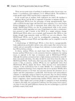
an array of programmable logic blocks embedded in a sea of programmable interconnect. This array is often referred to as the programmable logic fabric or just the
fabric. At the edges are programmable I/O blocks designed to interface the fabric
signals to the external world. It was this set of innovations that sparked the FPGA
industry. Figure 1.2 shows a basic architecture of an FPGA.
Interestingly, nearly all the other special FPGA features such as carry chains,
block RAM, or DSP blocks can also be implemented in programmable logic. This
is in fact the approach the initial FPGAs took and users did implement these functions in LUTs. However, as the FPGA markets developed, it became clear that these
special functions would be more cost effective as dedicated functions built from
hard gates and later FPGA families such as the Xilinx 4 K series and Virtex began
Fig. 1.2 Basic FPGA architecture
6
B. Taylor
to harden these special functions. This hardening improved not only cost but also
improved frequency substantially.
Within any one FPGA family, all devices will share a common fabric architecture, but each device will contain a different amount of programmable logic. This
enables the user to match their logic requirements to the right-sized FPGA device.
FPGAs are also available in two or more package sizes which allow the user to
match the application I/O requirements to the device package. FPGA devices are
also available in multiple speed grades and multiple temperature grades as well as
multiple voltage levels. The highest speed devices are typically 25 % faster than
the lower speed devices. By designing to the lowest speed devices, users can save
on cost, but the higher performance of the faster devices may minimize system
level cost.
Modern FPGAs commonly operate at 100–500 MHz. In general, most logic
designs which are not targeted at FPGA architectures will run at the lower frequency range, and designs targeted at FPGAs will run in the mid-frequency range.
The highest frequency designs are typically DSP designs constructed specifically to
take advantage of FPGA DSP and BRAM blocks.
Sections below describe a high level overview of FPGA architectures. Please
refer to Xilinx’s data sheets and user guides for more detailed and current
information.
1.5.2
Programmable Interconnect
Woven through the FPGA logic fabric is a set of wires which can be wired together
to connect any two blocks in an FPGA. This enables arbitrary logic networks to be
constructed by the user. The architecture of the interconnect wires varies from generation to generation and is hidden from the user by the tools.
1.5.3
Programmable Logic Block
An array of programmable logic blocks are embedded into the programmable
interconnect. These are called CLBs (configurable logic blocks) in Xilinx devices.
Today, each logic block consists of one or more programmable logic functions
implemented as a 4–6-bit configurable lookup table (LUT), a configurable carry
chain, and configurable registers. We use the word configurable to indicate a hard
block which can be configured through the FPGA’s configuration memory to be
used as part of the user’s logic. For instance, if the user design called for a register
with a clock enable (CE), the register is configured to have the clock enable enabled
and connected to the user’s CE signal. Figure 1.3a through c illustrates the
UltraScale CLB architecture, showing the CLB, LUT-flip-flop pair, and the carry
chain structures.
1
State-of-the-Art Programmable Logic
7
The combination of a LUT, carry chain, and register is called a logic cell or LC.
The capacity of FPGAs is commonly measured in logic cells. For instance, the
largest Xilinx Virtex UltraScale FPGA supports up to 4 million LCs, while the
smallest Spartan device contains as few as 2000 logic cells. Depending on usage,
each logic cell can map between 5 and 25 ASIC gates. The lower number is commonly used for ASIC netlist emulation, while the higher number is achievable under
expert mapping.
For Xilinx UltraScale devices, the CLB supports up to 8 × 6-input LUTs, 16 registers, and 8 carry chain blocks. Each 8-LUT can be configured as 2 × 5-LUTs if the
5-LUTs share common signals. For comparison purposes, Xilinx rates each 6-LUT
as the equivalent of 1.6 LCs or Logic cells.
Embedded in the CLB is a high-performance look-ahead carry chain which
enables the FPGA to implement very high-performance adders. Current FPGAs
have carry chains which can implement a 64-bit adder at 500 MHz.
Associated with each LUT is an embedded register. The rich register resources
of the FPGA programmable logic enable highly pipelined designs, which are a key
to maintaining higher speeds. Each register can be configured to support a clock
enable and reset with configurable polarity.
An important additional feature of the Xilinx CLB’s 6-LUT is that it can configure
to implement a small 64-bit deep by 1-bit wide memory called a distributed RAM.
An alternate configuration allows the 6-LUT to implement a configurable depth
shift register with a delay of 1–32 clocks.
1.5.4
Memory
Access to memory is extremely important in modern logic designs. Programmable
logic designs commonly use a combination of memories embedded in the FPGA
logic fabric and external DDR memories. Within the logic fabric, memory can be
implemented as discrete registers, shift registers, distributed RAM, or block RAM.
Xilinx UltraScale devices support two sizes of block RAM, 36-kbit RAMs and 288kbit RAMs. In most cases the Xilinx tools will select the best memory type to map
each memory in the user design. In some cases, netlists optimized for FPGAs will
hand instantiate memory types to achieve higher density and performance.
Special forms of memory called dual-port memories and FIFOs are supported as
special modes of the block RAMs or can be implemented using distributed RAM.
System memory access to external DDR memory (Chap. 5) is via a bus interface
which is commonly an AXI protocol internal to the FPGA. UltraScale FPGAs support
72-bit wide DDR4 at up to 3200 MB/s.
In general, registers or flip-flops are used for status and control registers, pipelining,
and shallow (1–2 deep) FIFOs. Shift registers are commonly used for signal delay
elements and for pipeline balancing in DSP designs. Distributed RAMs are
used for shallow memories up to 64 bits deep and can be as wide as necessary.
Block RAMs are used for buffers and deeper memories. They can also be aggregated
8
B. Taylor
CROSSBAR
SWITCH
LUT
#1
l0
FPGA ROUTING
CLB
l0
O0
O1
O2
l63
l7
O3
l56
O0
LUT
#8
O28
O29
O31
CROSSBAR
SWITCH
O30
l63
O31
Fig. 1.3 (a) UltraScale CLB, (b) one of the eight LUT-flip-flop pairs from an UltraScale CLB, (c)
carry chain paths
1
State-of-the-Art Programmable Logic
9
COUT
Carry Chain Block (CARRY8)
CO7
HMUX/HQ(1)
S7
O6 From LUTH
MUXCY
O7
O5 From LUTH
HMUX
D17
HQ
HX
(Optional)
CO6
S6
O6 From LUTG
GMUX/GQ(1)
MUXCY
O6
O5 From LUTG
GMUX
D16
D Q
GQ
GX
(Optional)
CO5
S5
O6 From LUTF
FMUX/FQ(1)
MUXCY
O5
O5 From LUTF
FX
FMUX
D15
D Q
FQ
(Optional)
CO4
S4
O6 From LUTE
EMUX/EQ(1)
MUXCY
O4
O6 From LUTE
EMUX
D14
D Q
EX
EQ
(Optional)
CYINIT
01
CO3
O6 From LUTD
S3
DMUX/DQ(1)
MUXCY
O3
O5 From LUTD
D13
DMUX
D Q
DX
DQ
(Optional)
CO2
O6 From LUTC
S2
CMUX/CQ(1)
MUXCY
O2
O5 From LUTC
D12
CMUX
D Q
CX
CQ
(Optional)
CO1
O6 From LUTB
S1
O6 From LUTB
D11
BMUX/BQ(1)
MUXCY
O1
BMUX
D Q
BX
BQ
(Optional)
CO0
O6 From LUTA
S0
AMUX/AQ(1)
MUXCY
O0
O5 From LUTA
D10
AX
CYINIT
CIN
01
CIN
Fig. 1.3 (conrinued)
AMUX
D Q
AQ
(Optional)
Note 1: Can be used it
unregistered/registered
outputs are free.
10
B. Taylor
Fig. 1.4 DSP flowgraph
together to support arbitrary widths and depths. For instance, a 64-bit wide by
32 K-bit deep memory would require 64 block RAMs. Generally FPGAs contain
around 1 36 K block RAMs for every 500–1000 logic cells.
1.5.5
DSP Blocks
Modern FPGAs contain discrete multipliers to enable efficient DSP processing.
Commonly DSP applications build pipelines or flow graphs of DSP operations and
data streams through this flow graph. A typical DSP filter called an FIR (finite
impulse response) filter is shown in Fig. 1.4. It consists of sample delay blocks,
multipliers, adders, and memories for coefficients. Interestingly this graph can be
almost directly implemented as an FPGA circuit.
For filtering and many other DSP applications, multipliers and adders are used to
implement the flow graph. Xilinx FPGAs contain a DSP block known as a DSP48
which supports an 18-bit × 25-bit multiplier, a 48-bit accumulator, and a 25-bit preadder. In addition up to four levels of pipelining can be supported for operation up
to 500 MHz. The DSP48 supports integer math directly; however, 32-bit and 64-bit
floating point operations are supported as library elements. A 32-bit floating point
multiplier will require two DSP48s and several hundred LCs.
Xilinx tools will generally map multipliers and associated adders in RTL or HDL
languages to DSP48 blocks. For highest performance however, designs optimized
for DSP in FPGAs may use DSP48 aware libraries for optimal performance, power,
and density.
1.5.6
Clock Management
Logic netlists almost universally require one or more system clocks to implement
synchronous netlists for I/O and for internal operation. Synchronous operation uses a
clock edge to register the results of upstream logic and hold it steady for use by
1
State-of-the-Art Programmable Logic
11
downstream logic until the next clock edge. The use of synchronous operation allows
for pipelined flow graphs which process multiple samples in parallel. External digital
communications interfaces use I/O clocks to transfer data to and from the
FPGA. Commonly, interface logic will run at the I/O clock rate (or a multiple of the
I/O clock rate). Chapter 12 covers more on clocking resources available on Xilinx
FPGAs.
1.5.7
I/O Blocks
One of the key capabilities of FPGAs is that they interface directly to external input
and output (I/O) signals of all types and formats. To support these diverse requirements, modern FPGAs contain a special block called the I/O block or IOB. This
block contains powerful buffers to drive external signals out of the FPGA and input
receivers, along with registers for I/O signals and output enables (OE). IOBs typically support 1.2–3.3 V CMOS as well as LVDS and multiple industry I/O memory
standards such as SSTL3. For a complete list, refer to the device datasheet. I/Os are
abstracted from the user RTL and HDL design and are typically configured using a
text file to specify each I/O’s signaling standard.
UltraScale devices also include multiplexing and demultiplexing features in the
I/O block. This feature supports dual data rate (DDR) operation and operation for
4:1 or 8:1 multiplexing and demultiplexing. This allows the device to operate at a
lower clock rate than the I/O clock. For example, Gigabit Ethernet (SGMII) operates at 1.25 GHz over a single LVDS link, which is too fast for the FPGA fabric to
support directly. The serial signal is expanded to 8/10 bits in the IOB interface to the
fabric allowing the fabric to operate at 125 MHz.
I/Os are commonly a limited resource, and FPGAs are available in multiple
package sizes to allow the user to use smaller lower-cost FPGAs with lower signal
count applications and larger package sizes for higher signal count applications.
This helps to minimize system cost and board space.
A primary application of FPGA I/Os is for interfacing to memory systems.
UltraScale devices support high-bandwidth memory systems such as DDR4.
1.5.8
High-Speed Serial I/Os (HSSIO)
CMOS and LVDS signaling are limited in performance and can be costly in terms
of power and signal count. For this reason, high-speed serial I/Os have been developed to enable low-cost, high-bandwidth interfaces. This evolution can be seen in
the evolving PCI standard which has moved from low-speed 32-bit CMOS interfaces at 33 MHz to PCIe Gen3 with 1–8 lanes at 8 Gb/s lane. An eight-lane PCIe
Gen3 interface can transfer 64 Gb/s of data in each direction. Xilinx UltraScale
devices support up to 128 MGT (Multi-Gigabit Transceivers) at up to 32.75 Gb/s.
12
B. Taylor
Within the FPGA, the HSSIO are interfaced directly to a custom logic block
which multiplexes and demultiplexes the signals to wide interfaces at lower clock
rates. This block also performs link calibration and formatting.
1.6
System on Chip
Current generation FPGAs now include an optional system on chip (SoC).
These are available in the Zynq-7000 devices as well as the UltraScale + MPSoC
devices. These SoCs include a state-of-the-art quad core ARM A53 application
processor, an external DDR DRAM interface, internal memory and caching
system, common I/O peripherals, and a set of high-bandwidth interfaces to
the FPGA programmable logic.
The SoC is built using ASIC technology and is competitive with discrete embedded
processors in cost and performance. It boots when powered up from an external
flash memory. The processor is then available to load the FPGA design. While booting, the CPU boot code is optionally decrypted and authenticated enabling secure
and safe embedded systems. Chapter 6 talks more about using these devices.
1.6.1
Operating System Support
The SoC system is capable of running bare-bones without an operating system
or running a real-time operating system ( RTOS ) or embedded OSs such as
Linux . It also supports asymmetric OSs where, for example, one core runs
Linux and the other core runs an RTOS. This capability is ideal for embedded
systems.
1.6.2
Real-Time OS Support
The MPSoC also includes a separate dual core ARM R5 processor. This processor
is optimized for real-time applications and can optionally run in lockstep for highreliability applications. The combination of the dual core R5 and the quad core A53
enables secure, high-reliability, real-time processing, while the A53 application
processor executes application code. This combination is ideal for embedded,
industrial, and military applications.
1
State-of-the-Art Programmable Logic
1.7
13
System Level Functions
In addition to the SoC and programmable logic array, FPGAs include system level
functions for configuring and monitoring FPGAs.
1.7.1
System Monitor
For industrial and embedded applications, it is desirable to be able to monitor the
voltage of system power supplies and various analog signals as well as the internal
temperature of the FPGA. This allows the FPGA to detect if the power rails are
within specified tolerance and allows the FPGA to know it is operating legally. For
this reason and also for security reasons, FPGAs incorporate a small multichannel
ADC (analog-to-digital converter). Chapter 16 covers more on system monitor.
1.7.2
Fabric Power Management
Before SoCs were introduced, FPGAs operated on a single power domain. Typically
several voltages are required for the FPGA, the logic power supply, the auxiliary
power supply, and the I/O power supplies. The FPGA fabric supports several features
which allow the user to manage and minimize system power. FPGA fabric power
consists of two types of power—static power which exists even if the device is not
operating and dynamic power which is a function of clock rates and data activity.
Static power is quite low at low temperatures but can rise to significant levels at maximum die temperatures. Additionally some speed and temperature grades have lower
static power than others. The -2L speed grade is designed to operate at lower voltage
levels enabling lower system power. The user has some flexibility to manage power by
throttling fabric clocks if idle and by lowering die temperature using fan control.
1.7.3
SoC Device Power Management
The SoC devices introduce some additional flexibility in power management if the
application allows for sometimes running in reduced functionality or idle modes.
The Zynq-7000 devices support independent PS (processing system) and PL (programmable logic) power domains. Thus, if the PL is idle, its power supply can be
removed. The MPSoCs support even finer-grained power domains and can be placed
into low-power modes with only the R5s operating. This allows system power as
low as 50 mW to be achieved for low-performance modes. Normal operation of the
SoC would be in the 1–3 W range and the PL could be in the 2–20 W range.
14
1.7.4
B. Taylor
Configuration
Both the PS SoC and the PL require configuration data to function. For the PS this
is boot code, and for the PL, it is called the bitstream data. FPGAs will commonly include
a dedicated block to configure the FPGA from various sources of bitstream data.
Xilinx supports boot over JTAG, over a dedicated serial or parallel interface and from
dedicated flash memory devices. In the SoC devices, configuration is supported by
a configuration controller in the SoC. Optionally UltraScale devices can be booted
over a PCIe interface, eliminating the cost of local flash storage and simplifying
system level configuration data management.
1.7.5
Security
FPGA security is a relatively new concern, but modern devices contain multiple security
features which are used to decrypt, authenticate, and monitor configuration data.
Encryption is used to obscure the configuration data which is stored in external
memory devices. This is valuable to protect user IP (intellectual property) as well as
to provide protection for passwords and keys embedded in the configuration data.
FPGAs now store one-time programmable encryption key (of up to 256 bits) which
is used to decrypt configuration data on the fly.
Today it is critical for system integrity to check configuration data for correctness before loading into the PL and SoC. The configuration controller optionally
does this by first checking to see if the boot code or bitstream can be authenticated.
The MPSoC devices support authentication of up to 4 K bits in hardware. If an
authentication fails, the device cannot be booted. The bitstream is authenticated
against a decryption key stored in external memory.
Additional features of MPSoC devices include tamper detection circuitry with
clock, power, and temperature monitoring. This can be used to deter attacks based
on operating the device outside of its legal operating conditions.
Within the Zynq UltraScale + PS, hardware is used to isolate various parts of the system. This can prevent the application code from overwriting the secure real-time code.
1.7.6
Safety
FPGAs are physical devices which are specified to operate under specific voltage
and temperature conditions. They have a designed lifetime of 10 years of operation after which they may fail in various ways. During normal operation cosmic
rays and alpha radiation from radioactive trace elements can upset device registers. For these reasons circuitry has been built into the FPGA to monitor configuration data changes due to upset or other effects. The FPGA configuration data is
1
State-of-the-Art Programmable Logic
15
monitored for a digital signature. If this changes unexpectedly, a signal is raised
which can reset the FPGA. Memories are particularly sensitive to upset, and all
PL block RAMs and the large PS memories have added parity bits to detect a
single event upset.
1.7.7
Debug
Getting a large FPGA to production is a challenging effort. In order to facilitate
debugging a dedicated JTAG interface is provided on the FPGA and PS. This interface has access to the FPGA configuration system and the PS memory map. It can be
used to download code and to test system level I/O interfaces. Cross-trigger circuitry
is available to debug SoC software and PL hardware simultaneously. The PS also
includes support for standard ICE debugging pods.
1.7.8
Performance Monitoring
The MPSoC includes a number of performance monitors which can check and measure
traffic on the AXI interconnect. For the PL these performance monitoring blocks
can be implemented in soft logic to monitor PL AXI events.