DSpace at VNU: Raman spectroscopy of Cu doping in Zn1-xCoxO diluted magnetic semiconductor
Bạn đang xem bản rút gọn của tài liệu. Xem và tải ngay bản đầy đủ của tài liệu tại đây (160.78 KB, 4 trang )
ISSN 1063 7850, Technical Physics Letters, 2009, Vol. 35, No. 11, pp. 990–993. © Pleiades Publishing, Ltd., 2009.
Original Russian Text © N.V. Volkov, E.V. Eremin, V.S. Tsikalov, G.S. Patrin, P.D. Kim, Seong Cho Yu, Dong Hyun Kim, Nguyen Chau, 2009, published in Pis’ma v Zhurnal
Tekhnicheskoі Fiziki, 2009, Vol. 35, No. 21, pp. 33–41.
Switching of Current Channels and New Mechanism
of Magnetoresistance in a Tunneling Structure
N. V. Volkov*, E. V. Eremin, V. S. Tsikalov, G. S. Patrin, P. D. Kim,
Seong Cho Yu, Dong Hyun Kim, and Nguyen Chau
Kirensky Institute of Physics, Siberian Branch, Russian Academy of Sciences, Krasnoyarsk, 660036 Russia
Siberian Federal University, Krasnoyarsk, 660041 Russia
Siberian State Aerospace University, Krasnoyarsk, 660041 Russia
Department of Physics, Chungbuk National Un Iniversity, Cheongju 361 763, Korea
Center for Materials Science, National University of Hanoi, 334 Nguen Trai, Hanoi, Vietnam
*e mail:
Received April 28, 2009
Abstract—We have experimentally studied the transport properties of a planar La0.7Sr0.3MnO3
(LSMO)/Mn depleted LSMO/MnSi tunneling structure, in which the Mn depleted LSMO layer plays the
role of a potential barrier between the conducting layers of LSMO and MnSi. The measurements were per
formed in geometry with the current direction parallel to the planes of interfaces in the tunneling structure.
It is established that the structure exhibits a nonlinear current–voltage characteristic and possesses a positive
magnetoresistance, the value of which depends on the tunneling current. It is suggested that specific features
of the transport properties of this structure are related to the phenomenon of current channel switching
between the conducting layers. The switching mechanism is based on the dependence of the resistance of the
tunneling junction between the conducting layers on the bias voltage and the applied magnetic field.
PACS numbers: 72.25. b, 73.40. c, 75.47. m
DOI: 10.1134/S1063785009110054
Magnetic tunneling junctions and the phenomena
of spin polarized tunneling from ferromagnetic layers
have been extensively studied in recent years [1]. This
interest is related to both potential practical applica
tions and a rich spectrum of new physical phenomena
related to a relationship between the spin polarized
electron transport and the magnetic subsystem of low
dimensional structures. Tunneling junctions have been
traditionally studied in geometry with the current per
pendicular to the planes of interfaces in the tunneling
structure. This geometry is simpler for a theoretical
analysis and the interpretation of experimental results.
However, the current in plane (CIP) geometry, in
which the current is parallel to the planes of interfaces,
is sometimes preferred for the practical purposes, in
particular, in the case of ferromagnet/semiconductor
hybrid nanostructures compatible with the traditional
CMOS technology. In addition, this geometry can be
expected to reveal new manifestations of the spin
dependent electron transport.
This Letter presents the results of an investigation,
in which the transport properties of a tunneling struc
ture have been measured in the CIP geometry.
The tunneling structure was manufactured using the
method of pulsed laser ablation of La0.7Sr0.3MnO3
(LSMO) and Si targets with deposition onto a (001)
oriented SiO2 substrate. According to this, 5 nm thick
Si layer and 500 nm thick LSMO layer were sequen
tially deposited onto the substrate heated to 500°C.
The as grown structure was immediately annealed in
an oxygen containing atmosphere at 800°C for 1 h. It
was expected that this technological process must
yield a structure, in which the lower layer of manga
nese monosilicide (MnSi) and the upper LSMO layer
are separated by an interfacial layer of manganese
depleted LSMO (LSMδO) with a thickness of about
5 nm (see the inset to Fig. 1). This composition pro
file must form due to a high coefficient of Mn diffu
sion in Si [2]. The LSMδO layer possesses dielectric
properties and plays the role of a potential barrier
between the conducting layers of LSMO and MnSi
(electrodes).
According to the results of magnetic measure
ments, the manganite film exhibits a transition to the
ferromagnetic (FM) state at a temperature of ~300 K.
X ray diffraction data show evidence for a predomi
nant (110) orientation of the LSMO layer, but it is
most probable that this layer is textured. The presence
of boundaries, which separate crystalline grains and
play the role of potential barriers, is confirmed by a low
conductivity of the LSMO film and a large contribu
tion of tunneling to the sample resistance. As for the
990
SWITCHING OF CURRENT CHANNELS AND NEW MECHANISM
lower layer, it is known that MnSi is characterized by
metallic conduction and exhibits a transition to the
FM state at about 30 K [3].
The transport properties of the samplers were stud
ied using a Model 2400 SourceMeter (Keithley Instru
ments). The current carrying contact pads were
formed on the upper surface of the structure using a
two component silver filled epoxide glue. The experi
mental geometry is schematically depicted in the inset
to Fig. 1. The resistance was measured in the regime of
stabilized current, while the current–voltage (I–V)
curves were obtained in the current sweep regime. The
magnetic field was applied in the plane of the struc
ture. The sample temperature T was set and kept accu
rate to within 0.1 K in the entire range studied.
The experimental data can be conditionally
divided into two parts, which refer to (i) nonlinear
transport properties and (ii) the effect of a magnetic
field on the conduction. Let us first consider features
of the conduction in the absence of an external mag
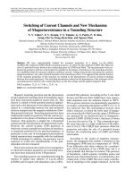
netic field. Figure 1 presents a series of I–V curves
measured at various temperatures. As can be seen, all
curves exhibit an almost linear initial portion. Then, at
a certain threshold current (Ith), the slope sharply
changes and, as the current I grows further, the voltage
increases at a slow rate. This behavior is especially
clearly pronounced at T < 30 K.
We propose the following model to interpret the
obtained I–V curves. In the given sample structure,
the upper layer (LSMO) possesses a higher resistance
than the lower (MnSi) layer. However, since the con
tact pads are formed on the upper surface and the
lower layer is separated from the upper by a potential
barrier, the current passes predominantly via the
LSMO layer. This is confirmed by the linear V(I)
dependence observed at small currents, in agreement
with what has to be expected for the manganite. An
increase in the current I and, hence, in the voltage
drop V between the contacts, leads to a redistribution
of charges in the lower conducting layer. This, in turn,
gives rise to a bias voltage Vb (Vb Ӷ V) on the tunneling
junctions under the current carrying contacts and the
related increase in the tunneling current IT through
the potential barrier separating the upper and lower
layers of the structure. Thus, the resistance RT of the
tunneling barrier decreases and the current begins to
flow predominantly via the lower (silicide) layer, the
resistance of which (RS) is small compared to that
(RM) of the manganite film.
The upper inset in Fig. 2 shows an equivalent electric
scheme of the tunneling structure in the CIP geometry.
The current through this circuit is determined by the
parallel connection of RM and the series of RT and RS.
According to this scheme, we have approximately
described the I–V curves by assuming that RS is small
compared to RT so that the charge transfer via the
TECHNICAL PHYSICS LETTERS
Vol. 35
No. 11
991
Voltage, V
T = 10 K
30
I+
15
LSMO
LSMδO
MnSi
I−
V+
V−
22 K
Vb
SiO2
0
30 K
90 K
160 K
−15
H=0
−30
−100 −75
200 K
250 K
−50
−25
0
25
50
75 100
Current, µA
Fig. 1. I–V curves of the tunneling structure measured at
various temperatures in the CIP geometry without an
external magnetic field. The inset shows a schematic dia
gram of the sample structure (arrows indicate the possible
current pathways).
lower layer is fully determined by the tunneling cur
rent (IT). This current was approximately described
using the Simmons formula [4] obtained in the
approximation of elastic electron tunneling through
the potential barrier:
1/2
IT = I0{ϕ0exp(–A ϕ 0 ) – (ϕ0 + eV)exp(–A(ϕ0 + eV)1/2)},
where ϕ0 is the potential barrier height, A is a coeffi
cient proportional to the barrier width Δx. The current
through the upper layer was described according to the
Ohm law as IM = V/RM, where RM was determined
from the temperature dependence of the sample resis
tance measured at I = Ith, that is, for the current pass
ing almost entirely through the manganite film. The
best fit was obtained for the following parameters:
potential barrier width Δx = 5 nm (this value well
agrees with the proposed structure composition); bias
voltage Vb ≅ 3 × 10⁻² V; and the average potential bar
rier height varying from ϕ0 ≅ 0.3 eV at T = 250 K to
ϕ0 ≅ 0.8 eV at T = 5 K.
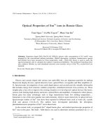
Figure 2 gives an example of the experimental I–V
curve approximated using the proposed model. The
lower inset shows the temperature dependence of ϕ0,
which can be determined by changes in the electron
structures of the tunneling junction components in the
course of FM ordering [5]. Some manganites [6]
exhibit an anomalously large change in the chemical
potential below TC, which is proportional to the
square of the sample magnetization. Thus, the work
2009
992
VOLKOV et al.
Voltage, V
150
(a)
100
T = 10 K
50
Voltage, V
15
10
RM
I+
RT
5
IM
IT
4
3
I−
1
RT
2
H=0
−50
ϕ0, eV
0.9
T = 30 K
−100
−150
MR
magnitude
3
0.6
−10
0.3
0
−15
−50
10 kOe
0
RS
0
−5
2 kOe
100
(b)
200 T, K
2 kOe
−25
0
25
50
Current, µA
Fig. 2. Example of the experimental I–V curve of the tun
neling structure in the CIP geometry at T = 30 K, approx
imated within the framework of the proposed model (with
an equivalent scheme in the upper inset): (1) experimental
points; (2) approximating curve; (3) I–V curve of the tun
neling junction; (4) I–V curve of the manganite layer. The
lower inset shows the temperature dependence of the aver
age potential barrier height ϕ0 in the structure, obtained
for the tunneling current approximated by the Simmons
formula.
2
1
10 kOe
0
−100
function of the LASMO layer upon the transition to
the FM state increases as compared to that of the
interfacial LSMδO layer (remaining in the nonmag
netic state), which plays the role of the potential bar
rier. As a result, ϕ0 increases with the magnetization of
LSMO, which explains the behavior observed at high
temperatures. The growth in ϕ0 at temperatures below
30 K is naturally explained by an increase in the work
function of the MnSi layer upon its transition to the
FM stage at T ~ 30 K.
The results of measurements of the I–V curves in
an external magnetic field H showed that the influence
of this field at T > 30 K is manifested only for I < Ith.
The effect of H in this interval of currents is fully deter
mined by the magnetoresistance (MR) of the LSMO
film. The MR is negative and its absolute value is inde
pendent of the probing current, which is typical of
manganites. For I > Ith, the sample exhibits switching
so that the current begins to flow predominantly via
the lower (silicide) layer. Since MnSi does not possess
significant MR, while the current via tunneling junc
tions at T > 30 K is independent of H, the MR effect
for I > Ith at T > 30 K is not observed. At T < 30 K, the
silicide layer exhibits magnetic ordering and the entire
−50
0
50
100
Current, µA
Fig. 3. LSMO/LSMδO/MnSi tunneling structure: (a) I–V
curves measured in the CIP geometry at T = 10K in the
absence of an external magnetic field (H = 0) and with an
applied magnetic field of H = 2 and 10 kOe; (b) plots of the
MR magnitude versus bias current for H = 2 and 10 kOe.
structure represents a magnetic tunneling junction.
The current through this junction depends on the
mutual orientation of magnetizations (MM and MS,
respectively) in the LSMO and MnSi layers.
As can be seen from the data in Fig. 3a, the effect of
the negative MR at T < 30 K for I < Ith is still retained,
but a strong influence of H is additionally manifested
in the I–V curves for I > Ith. Indeed, at T = 10 K, this
dependence already becomes linear in a field of H =
1 kOe, which can be interpreted as the reverse switch
ing of the current channel from the lower to upper
layer of the structure as a result of increase in the resis
tance RT of the tunneling junction in the applied mag
netic field. Indirect evidence for this scenario is the
negative MR (typical of the manganite film) observed
for I > Ith (see the MR curves for H = 2 and 10 kOe in
Fig. 3b).
Thus, there are several possibilities to control the
switching of current channels in a magnetic tunneling
structure in the CIP geometry. The bias voltage (cur
TECHNICAL PHYSICS LETTERS
Vol. 35
No. 11
2009
SWITCHING OF CURRENT CHANNELS AND NEW MECHANISM
rent) produces the current channel switching from the
upper to lower layer of the structure, while the external
magnetic field produces the reverse switching. The lat
ter factor determines the positive MR effect in the
magnetic tunneling structure according to an abso
lutely new mechanism, which has never been consid
ered until now. The proposed mechanism accounts for
the main features of manifestation of the MR effect; a
positive MR is induced by the bias current and its mag
nitude depends on this current. As can be seen from
Fig. 3b, the MR magnitude at T = 10 K and I = 100 μA
exceeds 300% and shows no tendency to saturation.
Considering the dependence of the tunneling cur
rent on the on the mutual orientation of magnetiza
tions in the FM layers (electrodes), we must take into
account that FM materials can be of the two types. In
the first case, charge carriers possess a preferred spin
orientation parallel to the magnetization and these
materials are referred to as majority spin carrier
(MASC) ferromagnets. In the second case, the spins
are predominantly oriented antiparallel to the magne
tization and these materials are referred to as minor
ity spin carrier (MISC) ferromagnets. In a tunneling
junction with one FM electrode of the MASC type
and the other electrode of the MISC type, the junction
resistance is greater for the parallel orientation of mag
netizations than for their antiparallel orientation [7].
Apparently, this situation takes place in the structure
under consideration. In the absence of a magnetic
field, the magnetostatic interaction results in the anti
parallel orientation of MM and MS, the junction resis
tance RT is at minimum, and the current at I > Ith flows
via the lower layer. An applied magnetic field tends to
orient MM and MS parallel to each other, RT increases
to become grater than RM, an the current even at I > Ith
passes predominantly via the upper layer with a linear
I–V curve.
TECHNICAL PHYSICS LETTERS
Vol. 35
No. 11
993
In conclusion, we studied the transport properties
of a tunneling structure in the CIP geometry and
revealed the phenomenon of current channel switch
ing between layers of the structure, which is controlled
by the bias current. At low temperatures, both elec
trodes in this structure occur in the FM state, in which
case the tunneling resistance can be controlled by an
applied magnetic field, which produces current chan
nel switching in the tunneling structure. These phe
nomena determine the new mechanism of MR, the
magnitude of which depends on the bias current in the
structure.
Acknowledgments. This study was supported by
the Russian Foundation for Basic Research (project
nos. 08 02 00259 and 08 02 100397) and the Minis
try of Education and Science of the Russian Federation
(program “Development of Scientific Potential of
Higher Education 2009–2010,” project no. 2.1.1/6038).
REFERENCES
1. J. C. Moodera and R. H. Meservey, Spin Polarized
Tunneling, in Magnetoelectronics, Ed. by. M. Johnson
(Elsevier, 2004).
2. G. Ctistis, U. Deffke, K. Schwinge, et al., Phys. Rev. B
71, 035 431 (2005).
3. Y. Ishikawa, G. Shirane, J. A. Tarvin, and M. Kohgi,
Phys. Rev. B 16, 4956 (1977).
4. J. G. Simmons, J. Appl. Phys. 34, 1793 (1963).
5. J. Klein, C. Hofener, S. Uhlenbruck, et al., Europhys.
Lett. 47, 371 (1999).
6. N. Furukawa, J. Phys. Soc. Jpn. 66, 371 (1997).
7. C. Mitra, P. Raychaudhuri, K. Dörr, et al., Phys. Rev.
Lett. 90, 017 202 (2003).
Translated by P. Pozdeev
2009