Analog Voltage Output
Bạn đang xem bản rút gọn của tài liệu. Xem và tải ngay bản đầy đủ của tài liệu tại đây (271.55 KB, 6 trang )
h t t p : / / r e s o u r c e . r e n e s a s . c o m Page 123
Chapter 10
Analog Voltage Output
Unlike A/D conversion, D/A conversion is designed to output analog
voltages. This conversion is easy to understand since it is simpler to use than
A/D conversion.
10.1 D/A Converter Configuration
In a microcomputer-applied system, an analog actuator (actuator which
controls physical values such as rotation speed and amount of generated heat
using analog voltages) may have to be controlled using analog voltages. Since
the microcomputer, however, is composed of digital circuits, it is incapable of
outputting analog voltages as they are.
Analog voltages, therefore, must be output after being converted from
several bits of digital numeric data. This conversion from digital to analog is
accomplished by the D/A converter, which is a peripheral function designed to
convert digital numeric data into analog voltages.
The H8/3048 D/A converter has the following characteristics:
Output voltage range 0V to 5V (max.)(range of analog voltages which can be output.)
Resolution 8 bits (refers to how many bits of digital numeric data voltages
are to be converted into.)
8-bit resolution means that voltages can be output in two to the
eighth power (256) steps within the output range.
Conversion time 10 microseconds (time required for conversion.)
An actuator capable of receiving analog voltages which change at
a time interval of 10 microseconds or longer can be controlled.
h t t p : / / r e s o u r c e . r e n e s a s . c o m Page 124
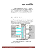
Figure 10.1: D/A Converter Block Diagram
The following explains the D/A converter configuration in the H8/3048.
It has 5 external pins. DA0 and DA1 are designed to output D/A converted
analog voltages. AVcc is a power supply pin and AVss is a ground pin. Since
they are separated from other power supply or ground pins, the D/A converter
will not function unless power is supplied to them. If you want to suppress
conversion errors, sufficient measures are also required in this case, too. V
REF
is
a reference voltage input pin for outputting voltages between AV
SS
and V
REF
with 8-bit (256-step) resolution.
There are two 8-bit D/A data registers (DADR0 and DADR1). When
analog output is enabled, data in the D/A data register are D/A converted for
output from the analog output pin.
10.2 D/A Converter Registers
Table 10.1 shows the D/A converter register configuration.
Table 10.1: D/A Converter Register Configuration
Each register is described below.
h t t p : / / r e s o u r c e . r e n e s a s . c o m Page 125
(1) D/A data registers 0 and 1 (DADR0 and DADR1)
The D/A data registers 0 and 1 (DADR0 and DADR1) are 8-bit,
read/write registers designed to store data to be D/A converted. Figure 10.2
shows the DADR0 as an example. The conversion results of data in the
DADR0 are output from the DA0 pin. Although the DADR1 has different
analog output pins and addresses, the use and meanings are completely the
same.
When analog output is enabled, the values in the DADR are always
D/A converted for output to the analog output pin.
Figure 10.2: D/A Data Register 0 (DADR0)
(2) D/A control register (DACR)
Figure 10.3 shows the D/A control register (DACR), which is operated
for D/A conversion. When the DACR is operated to enable analog output, data
in the DADR are D/A converted and analog voltages are always output from
the analog output pin. Output continues unless analog output is disabled. If the
values in the DADR are changed during output, the corresponding voltages are
output immediately after the conversion time has elapsed. Although the
maximum conversion time is 10 microseconds, it may take some time until the
output voltage reaches a certain level if the external circuit load is large.
Figure 10.3: D/A Control Register (DACR)
h t t p : / / r e s o u r c e . r e n e s a s . c o m Page 126
(3) D/A standby control register (DASTCR)
Figure 10.4 shows the D/A standby control register (DASTCR), which
is designed to enable or disable D/A output in software standby mode. The
details are not described here. Use it in default state.
Figure 10.4: D/A Standby Control Register (DASTCR)
1. You want to convert 10-bit digital numeric values into voltages in 1024
steps using the D/A converter. What do you do?
(A) Since the resolution of the D/A converter is fixed at 8 bits, they cannot
be converted into voltages in 1024 steps.
(B) Use the ADCR to change the resolution setting from the default of 8
bits to 10 bits.
(C) Multiply the 8-bit D/A conversion results by 1.25 (10/8).
Answer: (A)
(B) This is not available in the H8/3048.
(C) The D/A conversion results remain in 8-bit units (256 steps) even after this
multiplication.
2. How many methods can you use to start conversion by the D/A
converter?
(A) Only one method to externally input a signal.
(B) Only one method to use an instruction.
(C) Two methods to externally input a signal and use an instruction.
Answer: (B)
In the case of the H8/3048, conversion can only be started using an instruction.
3. From which pin are the voltages obtained by D/A converting numeric
data in the DADR1 output?
h t t p : / / r e s o u r c e . r e n e s a s . c o m Page 127
Answer: DA1 pin
Read "(1) D/A data registers 0 and 1 (DADR0 and DADR1)" in 10.2 to
understand the relationship between the DADR and the analog output pin.
4. You want to D/A convert both channels 0 and 1. How do you set the
upper 3 bits of the DACR?
Answer: Write B'011, B'010 or B'11-.
Understand how the DACR is used by referring to "Figure 10.3: D/A Control
Register (DACR)" in 10.2.
5. How is the DACR changed after the first D/A conversion of the specified
channel is completed?
Answer: There is no change
The H8/3048 has no flag to indicate that D/A conversion has been completed.
The DACR register is designed to enable or disable D/A conversion.
<D/A converters>
Write a program to use a D/A converter as you have learned in Chapter
10 and run it on the training board. Work out through the following steps:
• Complete the exercise source program by filling out its blanks.
• Make sure that the program runs successfully on the training board.
• If the program will not run as specified in the exercise, consult the
sample answer and make necessary changes to it before rerunning it.
The training board houses a circuit in which an operational amplifier
connected to the DA0 pin turns on an LED, so that the D/A converter output
voltage can control the brightness of the LED.
The higher the output voltage, the brighter the LED glows; the lower
the output voltage, the dimmer the LED becomes. A voltage of approximately
2 V is required to turn on the LED. The LED will stay out under an output
voltage of 0 to 2 V. Changes in the LED brightness would be more easily
identifiable visually by changing the output voltage from 1 V to 5 V.