Advanced Verification Flow part 1
Bạn đang xem bản rút gọn của tài liệu. Xem và tải ngay bản đầy đủ của tài liệu tại đây (40.01 KB, 11 trang )
[ Team LiB ]
15.1 Traditional Verification Flow
A traditional verification flow consisting of certain standard components is illustrated in
Figure 15-1
. This flow addresses only the verification perspective. It assumes that logic
design is done separately.
Figure 15-1. Traditional Verification Flow
As shown in Figure 15-1
, the traditional verification flow consists of the following steps:
1. The chip architect first needs to create a design specification. In order to create a
good specification, an analysis of architectural trade-offs has to be performed so
that the best possible architecture can be chosen. This is usually done by
simulating architectural models of the design. At the end of this step, the design
specification is complete.
2. When the specification is ready, a functional test plan is created based on the
design specification. This test plan forms the fundamental framework of the
functional verification environment. Based on the test plan, test vectors are applied
to the design-under-test (DUT), which is written in Verilog HDL. Functional test
environments are needed to apply these test vectors. There are many tools
available for generating and apply test vectors. These tools also allow the efficient
creation of test environments.
3. The DUT is then simulated using traditional software simulators. (The DUT is
normally created by logic designers. Verification engineers simulate the DUT.)
4. The output is then analyzed and checked against the expected results. This can be
done manually using waveform viewers and debugging tools. Alternately, analysis
can be automated by the test environment checking the output of the DUT or by
parsing the log files using a language like PERL. In addition, coverage results are
analyzed to ensure that the tests have exercised the design thoroughly and that the
verification goals are met. If the output matches the expected results and the
coverage goals are met, then the verification is complete.
5. Optionally, additional steps can be taken to decrease the risk of a future design re-
spin. These steps include Hardware Acceleration, Hardware Emulation and
Assertion based Verification.
Earlier, each step in the traditional verification flow was accomplished with Verilog
HDL. Though Verilog HDL remains the dominant method for creating the DUT, many
advances have occurred in the other steps of the verification flow. The following sections
describe these advances in detail.
15.1.1 Architectural Modeling
This stage includes design exploration by the architects. The initial model typically does
not capture exact design behavior, except to the extent required for the initial design
decisions. For example, a fundamental algorithm like an MPEG decoder might be
implemented, but the processor to memory bandwidth is not specified. The architect tries
out several different variations of the model and make some fundamental decisions about
the system. These decisions may include number of processors, algorithms implemented
in hardware, memory architecture, and so on. These trade-offs will affect the eventual
implementation of the target design.
Architectural models are often written using C and C++. Though C++ has the advantage
of object oriented constructs, it does not implement concepts such as parallelism and
timing that were found in HDLs. Thus, creators of architectural models have to
implement these concepts in their models. This is very cumbersome, resulting in long
development times for architectural models.
To solve this problem, architectural modeling languages were invented. These languages
have both the object oriented constructs found in C++ as well as parallelism and timing
constructs found in HDLs. Thus, they are well-suited for high-level architectural models.
A likely advancement in the future is the design of chips at the architectural modeling
level rather than at the RTL level. High-level synthesis tools will convert architectural
models to Verilog RTL design implementations based on the trade-off inputs. These RTL
designs can then go through the standard ASIC design and verification flow. Figure 15-2
shows an example of such a flow.
Figure 15-2. Architectural Modeling
Appendix E
, Verilog Tidbits, contains further information on popular architectural
modeling languages.
15.1.2 Functional Verification Environment
The functional verification of a chip can be divided into three phases.
•
Block level verification: Block level verification is usually done by the block
designer using Verilog for both design and verification. A number of simple test
cases are executed to ensure that the block functions well enough for chip
integration.
•
Full ChipVerification: The goal of full chip verification is to ensure that all the
features of the full chip described in the functional test plan are covered.
•
Extended Verification: The objective of the extended verification is to find all
corner case bugs in the design. This phase of verification is lengthy since the set o
f
tests is not predetermined and it may continue past tape-out.
During the functional verification phase, a combination of directed and random
simulation is used. Directed tests are written by the verification engineers to test a
specific behavior of the design. They may use random data, but the sequence of events
are predetermined. Random sequences of legal input transactions are used towards the
end of functional verifcation and during the extended verification phases in order to
simulate corner cases which the designer may have missed.
As Verilog HDL became popular, designers
[1]
started using Verilog HDL to both the
DUT and its surrounding functional verification environment. In a typical HDL-based
verification environment,
[1]
In this chapter, the words "designer" and "verification engineer" have been used
interchangeably. This is because logic designers perform block level verification and are
often involved in the full chip verification process.
•
The testbench consisted of HDL procedures that wrote data to the DUT or read
data from it.
•
The tests, which called the testbench procedures in sequence to apply manually
selected input stimuli to the DUT and checked the results, were directed only
towards specific features of the design as described in the functional test plan.
However, as design sizes exceeded million gates, this approach became less effective
because
•
The tests became harder and more time consuming to write because of decreasing
controllability of the design.
•
Verifying correct behavior became difficult due to decreasing observability into
internal design states.
•
The tests became difficult to read and maintain.
•
There were too many corner cases for the available labor.
•
Multiple environments became difficult to create and maintain because they used
little shared code.
To make the test environment more reusable and readable, verification engineers needed
to write the tests and the test environment code in an object oriented programming
language. High-Level Verification Languages (HVLs) were created to address this need.
Appendix E
, Verilog Tidbits, contains further information on popular HVLs.
HVLs are powerful because they combine the object oriented approach of C++ with the
parallelism and timing constructs in HDLs and are thus best suited for verification. HVLs
also help in the automatic generation of test stimuli and provide an integrated
environment for functional verification, including input drivers, output drivers, data
checking, protocol checking, and coverage. Thus, HVLs maximize productivity for
creating and maintaining verification environments.
Figure 15-3
shows the various components of a typical functional verification
environment. HVLs greatly improve the designer's ability to create and maintain each test
component. Note that Verilog HDL is still the primary method of creating a DUT.
Figure 15-3. Components of a Functional Verification Environment
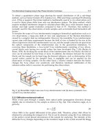
In an HVL-based methodology, the verification components are simulated in the HVL
simulator and the DUT is simulated with a Verilog simulator. The HVL simulator and the
Verilog simulator interact with each other to produce the simulation results. Figure 15-4
shows an example of such an interaction. The HVL simulator and Verilog simulator are
run as two separate processes and communicate through the Verilog PLI interface. The
HVL simulator is primarily responsible for all verification components, including test
generation, input driver, output receiver, data checker, protocol checker, and coverage
analyzer. The Verilog simulator is responsible for simulating the DUT.
Figure 15-4. Interaction between HVL and Verilog Simulators