Layout Plus Tutorial
Bạn đang xem bản rút gọn của tài liệu. Xem và tải ngay bản đầy đủ của tài liệu tại đây (288.58 KB, 14 trang )
CMPE 310
Fall 2006
Layout Plus Tutorial
Ekarat Laohavaleeson
Univerisity of Maryland, Baltimore County (UMBC)
1
Orcad Layout Plus Tutorial
Layout Plus is a circuit board layout tool that accepts a layout-compatible circuit
netlist (ex. from Capture CIS) and generates an output layout files that suitable for PCB
fabrication. This tutorial is the second part of PCB project tutorial. Before start with
Layout Plus, you need to have a complete netlist of your design, if you do not have it yet,
please read the first part on “Capture CIS Tutorial”.
Simple steps in producing PCB layout involve importing netlist, placing
components, routing and generating output files and reports. For more information about
Layout Plus, please refer to Layout Help (From Layout Plus menu, go to Help Æ Layout
Help)
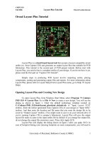
Opening Layout Plus and Creating New Design
To open Layout Plus, from Windows Start Menu, select Program Æ Cadence
PSD 15.0 Æ Layout Plus. Go to File Æ New to create a new design. You will see the
dialog as shown in figure 1. Enter the default technology template located on
C:\Cadence\PSD_15.0\tools\layout_plus\data\_default.tch in “Input Layout TCH”
textbox. Enter the netlist (generated from Capture CIS) of your design in “Input MNL”
textbox. And then enter the location and file name that you want the design file to be
saved in “Output Layout” textbox. (You might want to save it on your network drive if
you’re running Capture CIS in campus’s laboratory). Layout Plus will give the output
layout file name as same as the input netlist file by default. If you change the output file,
do not change the output file extension (.max). Then click Apply ECO.
Layout Plus will display the dialog shown in figure 2 after you apply ECO. In
case of footprint linking error (missing footprints on some components), you will need to
CMPE 310
Fall 2006
Layout Plus Tutorial
Ekarat Laohavaleeson
Univerisity of Maryland, Baltimore County (UMBC)
2
give the footprints to all missing components to complete AutoECO. (As explained in
Capture CIS tutorial, it is better to specify footprints to all parts during schematic
creation.) Hit “Accept this ECO” to import the netlist into Layout Plus. Figure3 shows
the Layout Plus window after importing a netlist.
Figure 1: New Design Dialog
CMPE 310
Fall 2006
Layout Plus Tutorial
Ekarat Laohavaleeson
Univerisity of Maryland, Baltimore County (UMBC)
3
Figure 2: Dialog after applied ECO
More info:
- ECO (Engineering Change Order) is Layout Plus command that provide an
ability to forward and back annotate your design flow. The forward annotate
let you forward the change of your netlist (ex., from Capture CIS schematic)
to the PCB. The back annotate just do the opposite, export the change of your
design in PCB back to the schematic.
- You can set different options for AutoECO, the tool will update particular
properties of the design according to the setting.
- Technology template (we are using _default.tch in this tutorial) contains
information regarding layout design such as board layers, spacing, track
widths, design rules, etc. Creating your own template is helpful in making a
number of designs with the same set of rules and settings however it is out of
this tutorial’s scope.
CMPE 310
Fall 2006
Layout Plus Tutorial
Ekarat Laohavaleeson
Univerisity of Maryland, Baltimore County (UMBC)
4
Figure 3: Layout Plus Window after importing netlist
Setting Design Environment
To set the design environment (display unit, grids, rotation, snap) go to Options
Æ System Settings. Modify the setting that suitable for your design. Figure 4 shows the
system setting dialog.
Next, you will need to define the layer stack for your design, go to View Æ
Database Spreadsheets Æ Layers. From here, specify layer type and mirror layer
(usually the most outer layers, TOP and BOTTOM, are the mirror layers of each other).
An example of layer stack for 4-layer board design (TOP, BOTTOM, POWER and
GND) with POWER and GND layers as power and ground plans and TOP and BOTTOM
as routing layers is shown in figure 5.
CMPE 310
Fall 2006
Layout Plus Tutorial
Ekarat Laohavaleeson
Univerisity of Maryland, Baltimore County (UMBC)
5
Figure 4: System Settings
After modify layer stack, you will need to specify routing spacing (Options Æ
Global Spacing), you can modify track-to-track, track-to-via, track-to-pad, via-to-via,
via-to-pad, and pad-to-pad spacing according to the capabilities of preferred PCB
manufacturer. (for example, www.pcbexpress.com ). Figure 6 shows all routing spacing
set to 6 mil.
There are many other parameters that you can set and should be carefully checked
with the recommended parameters from PCB manufacturer (drill sizes, padstacks,
minimum track width, etc.) In this tutorial we will use all default parameter values. If you
plan to fabricate your boards, please consult the PCB manufacturer.
More info:
- Mil unit is commonly used in PCB footprint and PCB board design.
- 1 mill = 0.001 inch