Tài liệu Cảm biến trong sản xuất P6 ppt
Bạn đang xem bản rút gọn của tài liệu. Xem và tải ngay bản đầy đủ của tài liệu tại đây (749.28 KB, 26 trang )
3 Sensors for Workpieces98
3.1.7
Further Reading
1 Adam, W., Busch, M., Nickolay, B., Senso-
ren für die Produktionstechnik; Berlin:
Springer, 1997.
2 Deutsche Gesellschaft für Zerstö-
rungsfreie Prüfung, Handbuch OF 1:
Verfahren für die Optische Formerfassung; Ei-
genverlag, 1995.
3 Dutschke, W., Fertigungsmeßtechnik; Stutt-
gart: Teubner, 1993.
4 Ernst, A., Digitale Längen- und Winkelmess-
technik; Landsberg/Lech: Verlag Moderne
Industrie, 1989.
5 Gasvik, K.J., Optical Metrology; Chichester:
J. Wiley, 1995.
6 Gevatter, H J., Handbuch der Mess- und
Automatisierungstechnik; Berlin: Springer,
1999.
7 Lemke, E.; Fertigungsmeßtechnik; Braun-
schweig: Vieweg, 1992.
8 Pfeifer, T., Fertigungsmeßtechnik; Munich:
Oldenbourg, 1998.
9 Schlemmer, H., Grundlagen der Sensorik;
Heidelberg: Wichmann, 1996.
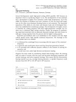
3.2
Micro-geometric Features
A. Weckenmann, Universität Erlangen-Nürnberg, Erlangen, Germany
Precision measurement of structures in the micrometer and sub-micrometer
ranges is becoming more and more important. Because of the never-ending min-
iaturization it is central to the precision of production and metrology of microelec-
tronics and micromechanics, but also to the measurement of the size distribution
of microparticles, for example, in environmental protection. A number of measur-
ing methods are available to perform these tasks. They range from conventional
optical microscopy and its extension into the ultraviolet range, through electron
microscopy, to the high-resolution near-field microscopy methods such as atomic
force microscopy.
Optical microscopy includes conventional bright- and dark-field microscopy,
confocal scanning microscopy, in the visible and ultraviolet spectral ranges, and
interference microscopy. As a non-microscopic additional feature, far-field diffrac-
tion images of the objects are evaluated. Fundamental research into the interac-
tion of the radiation used with the objects and theoretical modeling are impor-
tant, additional aids in using these methods. Non-optical, high-resolution micro-
scopy methods (scanning electron microscopy (SEM), atomic force microscopy
(AFM), etc.) are currently used to examine and assess the microgeometry of the
structures to be measured which cannot be resolved by light-optical methods, as a
supplement to optical measuring methods. After further extensive research into
the interaction of the scanning probes with the object structures and specific ex-
tension of microscope systems, eg, adding precision length measurement sys-
tems, high-resolution microscopy methods can also be used for calibration. So far
this has not been possible because the principle of optical methods places a limit
on the resolution that can be achieved.
Sensors in Manufacturing. Edited by H.K. Tönshoff, I. Inasaki
Copyright © 2001 Wiley-VCH Verlag GmbH
ISBNs: 3-527-29558-5 (Hardcover); 3-527-60002-7 (Electronic)
3.2.1
Tactile Measuring Method
Tactile measuring methods for surface measurement are still the most important
methods, especially in the area of metal-cutting and non-cutting machining opera-
tions in industry and research. It is the only operation that is anchored in na-
tional and international standards. Particularly the parameters and measurement
conditions are fixed, so that the comparability of the measurement results can be
secured. The surface roughness and topography greatly affect the mechanical and
physical properties of parts. Properties such as fit, seal, friction, wear, fatigue, ad-
hesion of coatings, electrical and thermal contact, and even optical properties
such as gloss, transparency, etc., can be adjusted by manufacturing design. The
surface laboratory is concerned with the assessment of roughness, waviness, tex-
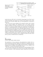
ture, groove depth, and other special surface shapes. The contact stylus method is
generally set-up off-line in the measuring room or in the workshop. Only in spe-
cial cases are oil-proof calipers integrated into the processing equipment. The pro-
file method is based on the linear sampling of the workpiece surface with a dia-
mond needle whose tip has the shape of a cone or a pyramid (Figure 3.2-1). The
radius of the tip is 2 and 10 lm and its angle usually 90 8.
The static measuring force applied is less than 1 mN. Thereby, equidistant pro-
file supporting points are measured directly to calculate various roughness and
waviness characteristics. The commencement of this method dates back to about
1930. Nowadays, measurement systems with digital signal processing and profile
evaluation are available. The instruments can be adjusted to fit the workpiece flex-
ibly by modularly compiling the stylus instrument, feed mechanism, and evalua-
tion system. Contact stylus instruments generally register a two-dimensional verti-
cal profile cut in the workpiece surface. Latterly, its application has expanded by
3.2 Micro-geometric Features 99
Fig. 3.2-1 Probe
tip (courtesy: PTB)
introducing a successive cross traverse for the three-dimensional measurement of
surface topography.
The amplitude resolution can be as good as 10 nm at any measurement point,
and the best possible local resolution in the horizontal axis is 0.25 lm. The mea-
suring range for contour measurements extends to 120 mm along the plane of
the face and 6 mm in amplitude. The contact stylus instrument is traceable to the
unit meter through reference standards.
Alignment of the cantilever is problematic. Additionally, the measuring instru-
ment is sensitive to vibrations and oscillations. A further problem in some cases
is a curved form of the surface of the workpiece.
For the adaptation of different workpiece geometries, a variety of different tac-
tile profile meters exist, whose properties clearly determine the quality of the sur-
face measurement. They can generally be traced back to the basic reference sur-
face, skidded and double skidded system.
3.2.1.1 Reference Surface Tactile Probing System
In the skidless system (Figure 3.2-2), the stylus is located at the end of a probing
arm that is guided over the surface of the object to be measured held in a linear
guide in the vertical direction. The styli are rigidly connected with a reference
plane that is usually located in the feed mechanism. The excursions of the stylus
caused by the surface roughness are transmitted to a measuring transducer and
converted to measuring signals, depending on the type of transducer, in analog or
digital format. The measuring pick-up and the object to be measured are me-
chanically decoupled, and only the stylus itself slides over the surface of the object
being measured. For that reason, skidless systems are extremely sensitive to vibra-
tions.
3.2.1.2 Skidded System
The skidded system (Figure 3.2-3) uses the surface to be measured as a guide and
has much smaller dimensions than the skidless system. The stylus contacts the
surface to be measured with a skid and acquires the surface profile relative to the
path of the skid with the probe tip. Depending on the measurement task, the
3 Sensors for Workpieces100
Fig. 3.2-2 Skidless system
landing skid is mounted before, behind, or lateral to the probe tip. The unavoid-
able distance between the landing skid and the probe tip can lead to falsifications
during the transfer of the profile, depending on the surface attributes of the work-
piece to be measured. However, it is less precise because of the mechanical filter-
ing that occurs while sliding over the surface. The skids act as an amplitude-inde-
pendent, non-linear, high-pass filter and eliminates, depending on the probe and
workpiece geometry, the macro-geometric form and waviness of the workpiece
profile. This system is used for fast measurements in production.
3.2.1.3 Double Skidded System
The double skidded system (Figure 3.2-4) uses the surface under test as a refer-
ence, it is self-aligning, insensitive to vibrations, and requires large measuring
surfaces because of its size.
The double skidded system can lead to considerable profile falsification owing
to its landing skid, especially with profile tips that jut out.
3.2.2
Optical Measuring Methods
Optical 3D measuring methods permit fast, wide-area sampling point acquisition.
In several measurements from different views, it is possible to measure all wear-
ing zones and zones of the workpiece relevant to determining the form and sur-
face characteristics of the workpiece with the required resolution. After transfor-
mation of the measured data into a common coordinate system, the sample is re-
presented by a 3D set of sampling points. From the measured data it is possible
to determine the form, surface, or wear characteristics. The advantages of this
3.2 Micro-geometric Features 101
Fig. 3.2-3 Skidded system
Fig. 3.2-4 Double
skidded system
method are that the measuring process can be automated to a great extent and is
therefore independent of the influences of the operator, it has a high measuring
rate, and the surface of the measured object is acquired as a whole. Especially
suitable for measured value acquisition for microgeometry are devices that oper-
ate on the principle of white-light interferometry or scattered light methods.
3.2.2.1 White Light Interferometry
Special white light interferometers permit wide-area form acquisition on optically
rough surfaces. A measuring system called coherence radar is based on the princi-
ple of the Michelson interferometer, where the mirror in the measuring beam is
replaced by the object to be measured. The light-emitting diode (LED) to be used
as the light source causes white light interference that displays a typical modula-
tion as a function of the phase shift between the measuring and reference beam,
which is at a maximum when no phase shift exists, ie, the object being measured
is in the reference plane (Figure 3.2-5).
Using a linear table, the object to be measured is pushed through the reference
plane and the position of the linear table is stored as a vertical coordinate for each
sampling point as soon as the maximum modulation of the interference signal ac-
quired with a charge-coupled device (CCD) camera is detected. One advantage of
this measuring method is that, unlike, for example, the triangulation method, illu-
mination and observation are in the same direction, which makes measurements
possible on structures with a large aspect ratio that are often encountered in mi-
crosystem technology. Both the topography of the measured object and, derived
from it, the roughness of its surface can be measured.
3 Sensors for Workpieces102
Fig. 3.2-5 Principle of a white light interferometer
Depending on the optical arrangement, measuring fields from about 50´ 50
mm to about 200´ 200 lm can be implemented. The lateral resolution depends
on the measuring field and the number of columns or rows of the CCD camera
(typically 512´ 512 pixels) and the pixel geometry; the resolution in the longitudi-
nal direction is limited by the roughness of the workpiece surface and the travers-
ing speed of the linear table (typically 1–2 lmat4lm/s). The measuring time is
in the minutes range, depending on the maximum structure depth to be mea-
sured.
3.2.2.2 Scattered Light Method
The scattered light method is used to measure the roughness of workpiece sur-
faces. Light reflected from the workpiece has a spatial distribution that depends
on the surface roughness. Smooth surfaces reflect incident light fully according to
the law of reflection of geometric optics (angle of reflection with respect to the
surface normal equal to the angle of incidence). On rough surfaces, portions of
the scattered light are also reflected in other directions. Figure 3.2-6 shows the ar-
rangement principle of a scattered light sensor. The collimated light of an LED is
deflected on to the workpiece surface via a beam divider. The diameter of the
measuring spot is about 1 mm. The scattered light is mapped with a lens on to a
linear image sensor (photodiode or CCD line) so that the intensity of the light
scattered in different directions can be measured at different locations on the de-
tector. To assess the surface, the scatter value S
N
is usually used. This is propor-
tional to the second statistical moment of the measured intensity distribution and
therefore describes its width. Larger S
N
values indicate a greater proportion of
scattered light, usually describing a rougher surface. One problem with the accep-
tance of this measuring method is that the measured S
N
value does not correlate
3.2 Micro-geometric Features 103
Fig. 3.2-6 Block diagram
of a scattered light sensor
with the roughness quantities R
a
and R
z
which have been introduced into tactile
roughness metrology and which are standardized.
3.2.2.3 Speckle Correlation
Speckle correlation differs between two methods: angular speckle correlation
(ASK) and spectral speckle correlation (SSK). Both methods use the correlation
coefficient of two takes of the surface as a measure for the roughness value R
q
.
This roughness value is equal to the standard deviation of the altitude values, so
that a mathematical connection between this and the correlation of different
speckle pictures exists as shown in statistical calculations.
Angular speckle correlation (ASK). Angular speckle correlation offers two advan-
tages. On the one hand, the requirements for the laser system are small, since
only one wavelength is necessary for the implementation of the measurement. On
the other hand, owing to the difference in the angles of illumination, the mea-
surement area can continuously be re-adjusted according to the measurement
task. The disadvantages of an adjustable difference angle result in high require-
ments for the mechanical precision. Figure 3.2-7 displays a typical experimental
set-up for ASK measurements with an adjustable difference angle. One of the illu-
mination beams is faded out when taking the first picture, and for the second pic-
ture the other is faded out. It is necessary to move one of the pictures respective
to the deviating illumination angle of the applied ASK, so that the offset opposite
the second picture can be counter-balanced. The distance moved can roughly be
3 Sensors for Workpieces104
Fig. 3.2-7 Setup of an angular speckle correlation
calculated from the geometry of the setup and is always the same for a fixed set-
up. The exact value can be calculated in an evaluation program.
Spectral speckle correlation (SSK). The setup of SSK is simplified to the extent that no
second illumination beam path is necessary. The adjustment of the measurement
system during practical application is far easier and one can achieve an increase
in stability. With the possibility of taking two pictures of the surface at the same
time, the measurement time can be reduced. The disadvantage of this measurement
system is the higher requirements for the laser system. At least two different wave-
lengths must be generated, so that an adaptation of the different roughness areas
becomes possible. A larger number of wavelengths is, however, more advantageous.
The evaluation of the two pictures taken takes place via a two-dimensional
cross-correlation coefficient. Experimental prerequisites for the correct evaluation
consist in the observance of Shannon’s theorem. This means that the spatial sam-
pling frequency, in this case the reciprocal pixel size of the CCD camera, has to
be at least twice as large as the spatial signal frequency. In other words,
d
speckle
> 2d
pixel
3:2-1
d
speckle
4
p
Á
kf
2x
0
3:2-2
where k is the wavelength of the light used, f the focal length of the lens and x
0
the diameter of the illuminated area on the surface.
3.2.2.4 Grazing Incidence X-Ray Reflectometry
The total reflection of X-rays from solid samples with flat and smooth surfaces
was first reported by Compton in 1923, which can be assumed to mark the birth
of the experimental technique of X-ray specular reflectivity. Since the angle of inci-
dence is very shallow and almost parallel to the surface, measurement using X-ray
total reflection is also called the grazing incidence experiment. If the surface is
not ideally smooth but somewhat rough, the X-rays can be diffusely scattered in
any direction. The experimental technique is known as X-ray diffuse scattering (X-
ray non-specular reflection). Its development began immediately after the pioneer-
ing work in 1963 of Yoneda, who reported intensity modulation in X-ray diffuse
scattering, known as Yoneda wings or anomalous reflection.
Nowadays, X-ray reflectometry based on total reflection has become a powerful
tool for the analysis of surfaces and thin-film interfaces, and will continue with
further progress. This is mainly due to the significant development of experimen-
tal techniques and instrumentation, especially the advent of synchrotron radiation
and the progress achieved in detector technology. The advances in theoretical
modeling and techniques for analyzing experimental data are also important.
Total reflection and the penetration capability of energy-rich X-rays are used for
coating thickness measurement. The refractive index for X-rays is always <1. If
3.2 Micro-geometric Features 105
the angle of incidence is made smaller, the X-radiation penetrates only up to a
very small angle, the critical angle. If the angle of incidence is reduced still
further, external total reflection on the interface occurs. The beam is reflected as
by a mirror. In coating-substrate systems, part of the radiation is reflected and
part of it penetrates the film. There are now two angles of total reflection at the
air-coating and coating-substrate interfaces. The two partial beams interfere and
form interference. Surface roughness and the optical densities of coating and sub-
strate material affect the acuity of the resulting interference image. The most in-
tense and sharpest interference images are obtained if the refractive index of the
substrate material is less than the refractive index of the coating material.
The main limitations of the X-ray reflectivity technique are the limited range of
the wave-vector transfer and the loss of the phase of the reflected amplitude.
Nevertheless, an accuracy of approximately 0.2 nm has been reported in determin-
ing the thickness and roughness of a double-layer sample.
3.2.3
Probe Measuring Methods
Over the last decade, fundamental research into surface physics has given rise to
a new class of analyzer, the scanning probe microscope. These devices allow the
mapping of a surface in a lateral range of 150´ 150 lm down to atomic resolution
according to similar measuring principles with slight technical variations. Fig-
ure 3.2-8 shows the principle of the structure of a scanning probe microscope.
Other members of this class are the magnetic force microscope, the optical
near-field microscope and microscopes that work by a thermal or capacitive inter-
face or with ion flows.
However, scanning probe microscopes are not only useful for characterizing
surfaces with high spatial resolution. The sharp tips of the scanning tunneling,
3 Sensors for Workpieces106
Fig. 3.2-8 Schematic of scanning probe microscopy (SPM)
scanning force, and lateral force microscopes can also be used as local sensors
and as nano-tools for carrying out experiments or for making surface modifica-
tions on the atomic scale. In this way, time-stable atomic-scale structures can be
generated, modified, and removed under environmental conditions. Chemical re-
actions can be induced locally with the AFM tip and crystal growth can be moni-
tored in situ and in real time. Forces and interactions can be investigated on the
(sub)atomic scale and the phenomenon of energy dissipation due to friction can
be studied quantitatively on a microscopic scale.
3.2.3.1 Scanning Electron Microscopy (SEM)
In many areas of research it is important to obtain chemical, morphological infor-
mation in the sub-micrometer range. Because of the limited resolution of optical
microscopes (theoretically 0.15 lm), bundled electrons accelerated by electrical
high voltage (up to 3 MV) in a high vacuum are used instead of light because
they are strongly deflected by scattering at atmospheric pressure. Rotationally
symmetric electrical and magnetic fields perform the same functions as lenses in
an optical microscope, concentrating the electron beam coming from the hot cath-
ode on to the object. The object to be measured is penetrated by the electrons to
different degrees in the transmission electron microscope depending on the thick-
ness and density of the electrons in such a way that the corresponding intensity
distribution in the electron image represents the structure. The electron image is
acquired on a photographic plate or fluorescent screen, yielding an approximately
200000-fold magnification. In SEM (Figure 3.2-9), an electron beam (diameter
about 10 nm) is moved over the object in a scanning pattern, ie, row by row. The
electrons, both those scattered back and the secondary electrons that escape from
the surface of the sample, are amplified by the scintillator and photomultiplier
and provide the signal for brightness control of a synchronously controlled cath-
ode-ray tube (large depth of field).
The resolution limit is determined by the diffraction phenomena at the aper-
ture of the imaging system and the wavelength of the particles. With a 100 kV
electron microscope, a resolution of 0.2 nm (k =3.7 pm, A=0.4–0.8, error of lens
aperture C
s
=0.3–1 mm) is achieved according to the equation
d
theor:
A Á
kC
s
4
p
: 3:2-3
3.2 Micro-geometric Features 107
3.2.3.2 Scanning Tunneling Microscopy (STM)
In scanning tunneling microscopy, a conductive, atomically sharp needle is
guided row by row over a conductive surface. If the probe is lowered near the sur-
face to be measured, interaction due to the quantum physical tunneling effect oc-
curs with the surface in the form of tunneling current (Figure 3.2-10). To obtain a
measurable signal, the distance from the tip to the sample must only be about
10 Å. With highly sensitive amplifiers, it is possible to detect currents up to 2fA
(10
–15
A). Influences from vibrations with amplitudes up to 1 lm (floor or sonic
vibrations) and thermal drift of the components in the range of approximately
0.1 lm/cm are problems encountered in implementing this measuring method.
It is possible to choose between two different modes. If, during the measuring
operation, the height of the tip is controlled in such a way that the tunneling cur-
rent remains constant (I
T
(x, y)= constant), the probe displacement in the vertical
direction provides a measure of the profile height of the surface at the measuring
point (Figure 3.2-11).
In the second mode, the height of the needle tip is kept constant
(Z
T
(x, y)= constant) and the variation in tunneling current is acquired during the
3 Sensors for Workpieces108
Fig. 3.2-9 Design of a scanning electron microscope
Cathode Tungsten or Lanthanum Hexaboride
measuring process (Figure 3.2-12). With this mode, however, there is a danger
that the tip might come into contact with the surface because of irregularities of
the sample and that incorrect measured current values could be obtained because
of electrical contact.
The advantage of this measuring method is its very high resolution of about
0.01 nm. The disadvantage is its low measuring range (laterally maximum
100 lm, in the z-direction maximum 10 lm).
3.2 Micro-geometric Features 109
Fig. 3.2-10 Schematic represen-
tation of tip and sample
interactions (tunneling effect)
Fig. 3.2-11 Constant-current
mode
Fig. 3.2-12 Constant-height
mode
3.2.3.3 Scanning Near-field Optical Microscopy (SNOM)
SNOM is high-resolution optical microscopy implemented by scanning a small
spot of ‘light’ over the specimen and detecting the reflected (or transmitted) light
for image formation (Figure 3.2-13). This is the only similarity with confocal mi-
croscopy, where the focal point is scanned. Operation of conventional light micro-
scopes suffers from the diffraction limit, which limits the optical resolution of the
microscope to only approximately a half wavelength of the light being used. The
resolution of the SNOM image is defined by the size and the properties of the
aperture, not by the wavelength used. This means that SNOM provides an im-
provement in spatial resolution of at least one order of magnitude over conven-
tional optical microscopes. However, the attainable resolution of approximately
50 nm is smaller than that for STM or AFM. SNOM utilizes tiny apertures of di-
ameters in the range typically 50–100 nm, ie, smaller than half the wavelength of
visible light. Typically such apertures are prepared in the metal coating at the
apex of an optically transparent, sharp tip. Light cannot pass through such an
aperture, but an evanescent field, the optical near-field, extends from it. The opti-
cal near-field decays exponentially with the distance, and is thus only detectable in
the immediate vicinity of the tip.
The optical resolution limit for SNOM is governed by the light intensity passing
through the aperture, usually by heating and pulling a fabricated fiber tip. A prac-
tical limit is usually encountered at aperture diameters between 80 and 200 nm
but in ideal cases diameters down to < 20 nm have been achieved.
If the aperture is brought close to the sample surface, the presence of the sam-
ple causes a disturbance of the optical near-field, which leads to the emission of
light from the location opposite the aperture. Scanning the aperture at a distance
of typically 10 nm from the sample with an accuracy of *5 Å, in order to prevent
3 Sensors for Workpieces110
Fig. 3.2-13 Design of SNOM in combination with AFM
damage to the tip and/or sample, and simultaneously detecting emitted light in
either the reflection or transmission mode produces a high-resolution optical im-
age. By contrast, conventional optical microscopy relies on observation in the far-
field where the achievable resolution is limited by diffraction.
SNOM instruments are technically closely related to scanning force and tunnel-
ing microscopes (SFM and STM) because probing involves scanning either the
probe tip or the sample with tip-to-sample distance control.
3.2.3.4 Scanning Capacitance Microscopy (SCM)
Scanning capacitance microscopy (SCM) images spatial variations in capacitance
(Figure 3.2-14). Like EFM (see Section 3.2.3.11), SCM induces a voltage between
the tip and the sample. In the first mode, the cantilever operates in a non-contact,
constant-height mode. A special circuit monitors the capacitance between the tip
and the sample. Since the capacitance depends on the dielectric constant of the
medium between the tip and sample, SCM studies can image variations in the
thickness of a dielectric material on a semiconductor substrate. SCM can also be
used to visualize sub-surface charge-carrier distributions, eg, to map dopant pro-
files in ion-implanted semiconductors.
In addition to measuring surface topography, the probe tip can also be used as
a proximal probe. In the second mode, the probe tip is kept in contact with the
surface to generate a topographic image. In addition, AC and DC voltages are ap-
plied between the tip and a semiconductor sample. Changes in the capacitance of
the semiconductor beneath the probe tip are measured using a special sensor.
Changes in the capacitance are mapped simultaneously with topography. These
changes can be correlated with the dopant type and concentration of the semicon-
ductor.
3.2.3.5 Scanning Thermal Microscopy (SThM)
In scanning thermal microscopy (SThM), a microscopically small wire loop as the
detector is scanned over the sample surface, without coming into contact with the
sample. Figure 3.2-15 shows the structure of a tip.
3.2 Micro-geometric Features 111
Fig. 3.2-14 Working principle of SCM
In addition to topography representation, which is analogous to that in AFM,
thermal sample properties can also be acquired with a positional resolution in the
nanometer range. If, for example, such a small current is conducted through the
wire loop (see Figure 3.2-15) that no self-heating occurs, the local sample tempera-
ture can be derived from the resistance of the wire loop. If the current is in-
creased so that a temperature difference between the tip and sample arises, it is
possible to derive the local thermal conductivity directly from the measurable heat
flow from the tip to the sample.
Thermal conductivity imaging is achieved using a special probe to measure
both the topography and temperature. Using a Wollaston wire (which acts as a re-
sistor in a Wheatstone bridge circuit), the surface is scanned with a second feed-
back signal that applies power to the probe keeping the temperature between the
probe and sample constant. Variations in surface conductivity cause heat-flow
changes in or out of the probe. These are recorded as a thermal conductivity map
enabling individual phases of blends to be mapped.
The second possible design of a tip for SThM is a cantilever composed of two
different metals, presented by Digital Instruments (a thermal element made up of
two metal wires can also be used). The materials of the cantilever respond differ-
ently to changes in thermal conductivity, and cause the cantilever to deflect. The
system generates an image, which is a map of the thermal conductivity, from the
changes in the deflection of the cantilever. A topographical non-contact image can
be generated from changes in the cantilever’s amplitude of vibration. Thus, topo-
graphic information can be separated from local variations in the sample’s ther-
mal properties, and the two types of images can be collected simultaneously.
Temperature Resolution. Typical temperature resolution of 0.28C after temperature
calibration of the probe is observed. Temperature calibration is probe dependent.
The temperature resolution of the probe is currently limited by the electrical
noise of the sensor.
Spatial Resolution. The measured spatial resolution of SThM is dependent on the
characteristics of the sample, with the best observed resolution of 150–200 nm
full width at half maximum (FWHM), as measured on electrically biased magne-
toresistive stripes of magnetic data storage read elements. Note that three main
3 Sensors for Workpieces112
Fig. 3.2-15 Design of a tip for
scanning thermal microscopy
factors affect the apparent spatial resolution of imaged temperature gradients:
heat spreading in the sample due to thermal insulation properties of the back-
ground sample material versus the heat source; spatial extent of the heat source;
and distance of the probe tip to the actual thermal source relative to the surface
being imaged.
Samples which give the best apparent thermal spatial resolution (and therefore
have the largest thermal gradients) have small heat sources in a thermally insulat-
ing substrate with the thermal source very close to the surface being imaged.
Ideal samples also provide adequate electrical insulation between the circuit of in-
terest and the probe sensor.
3.2.3.6 Atomic Force Microscopy (AFM)
Atomic force microscopy (AFM) probes the surface of a sample with a sharp tip,
about 10 lm long and often less than 100 Å in diameter. The tip is located at the
free end of a cantilever that is 100–200 lm long (Figure 3.2-16).
3.2 Micro-geometric Features 113
Fig. 3.2-16 Top and side view of a tip, tip height about 5–7 lm (courtesy: ThermoMicroscopes)
Forces between the tip and the sample surface cause the cantilever to bend or
deflect. A detector measures the cantilever deflection as the tip is scanned over
the sample, or the sample is scanned under the tip. The measured cantilever de-
flections allow a computer to generate a map of surface topography. In contrast to
SEM, AFM can be used to study insulators and semiconductors as well as electri-
cal conductors without special and expensive preparation of the specimen. The
typical scan range of such an instrument is approximately 120 lm laterally and
about 5 lm vertically.
Several forces typically contribute to the deflection of an AFM cantilever. The
force most commonly associated with AFM is an interatomic force called the van
der Waals force. The dependence of the van der Waals force upon the distance be-
tween the tip and the sample is shown in Figure 3.2-17.
Two distance regimes are labeled on Figure 3.2-17: (1) the contact regime and
(2) the non-contact regime. In the contact regime, the cantilever is held less than
a few ångströms from the sample surface, and the interatomic force between the
cantilever and the sample is repulsive. In the non-contact regime, the cantilever is
held tens to hundreds of Ångströms from the sample surface, and the interatomic
force between the cantilever and sample is attractive (largely a result of the long-
range van der Waals interactions). Both contact and non-contact imaging tech-
niques are described in detail below.
Contact AFM. In the contact AFM mode (C-AFM), also known as the repulsive
mode, an AFM tip makes soft ‘physical contact’ with the sample. The tip is at-
tached to the end of a cantilever with a low spring constant (0.6–2.8 N/m), lower
than the effective spring constant holding the atoms of the sample together. As
the scanner traces the tip across the sample (or the sample under the tip), the
contact force causes the cantilever to bend to accommodate changes in topogra-
phy. Even if a very stiff cantilever is designed to exert large forces on the sample,
the interatomic separation between the tip and sample atoms is unlikely to de-
crease much. Instead, the sample surface is likely to deform (nanolithography). In
addition to the repulsive van der Waals force, two other forces are generally pres-
ent during contact AFM operation: a capillary force exerted by the thin water layer
often present in an ambient environment, and the force exerted by the cantilever
itself. The capillary force arises when water wicks its way around the tip, applying
a strong attractive force (about 10
–8
N) that holds the tip in contact with the sur-
3 Sensors for Workpieces114
Fig. 3.2-17 Interatomic force
versus distance curve
face. The magnitude of the capillary force depends on the tip-to-sample distance.
The force exerted by the cantilever is like the force of a compressed spring. The mag-
nitude and sign (repulsive or attractive) of the cantilever force depend on the deflec-
tion of the cantilever and on its spring constant. As long as the tip is in contact with
the sample, the capillary force should be constant because the distance between the
tip and the sample is virtually incompressible, assuming that the water layer is rea-
sonably homogeneous. The variable force in C-AFM is the force exerted by the can-
tilever. The total force that the tip exerts on the sample is the sum of the capillary
plus cantilever forces, and must be balanced by the repulsive van der Waals force
for C-AFM. The magnitude of the total force exerted on the sample varies from
10
–8
N (with the cantilever pulling away from the sample almost as hard as the
water is pulling down the tip), to the more typical operating range of 10
–7
–10
–6
N.
Usually AFMs detect the position of the cantilever with optical techniques. In the
most common scheme, shown in Figure 3.2-18, a laser beam bounces off the back
of the cantilever on to a position-sensitive photodetector (PSPD).
The PSPD itself can measure displacements of light as small as 10 Å. The ratio of
the path length between the cantilever and the detector to the length of the cantilever
itself produces a mechanical amplification. As a result, the system can detect sub-
ångström vertical movement of the cantilever tip. Other methods of detecting canti-
lever deflection rely on optical interference or even a scanning tunneling microscope
tip to read the cantilever deflection. Another technique is to fabricate the cantilever
from a piezoresistive material so that its deflection can be detected electrically (strain
from mechanical deformation causes a change in the material’s resistivity). In that
case, a laser beam and a PSPD are not necessary. Once the AFM has detected the
cantilever deflection, it can generate the topographic data set by operating in one
of two modes – constant-height or constant-force mode. In the constant-height
mode, the spatial variation of the cantilever deflection can be used directly to gener-
ate the topographic data set because the height of the scanner is fixed as it scans. In
the constant-force mode, the deflection of the cantilever can be used as input for a
feedback circuit that moves the scanner up and down in z, responding to the topo-
graphy by keeping the cantilever deflection constant. In that case, the image is gen-
erated from the scanner’s motion. With the cantilever deflection held constant, the
total force applied to the sample is constant. In the constant-force mode, the scan-
ning speed is limited by the response time of the feedback circuit, but the total force
3.2 Micro-geometric Features 115
Fig. 3.2-18 The beam-bounce detection scheme
exerted on the sample by the tip is well controlled, generally preferred for most ap-
plications. The constant-height mode is often used for taking atomic-scale images of
atomically flat surfaces, where the cantilever deflections and thus variations in ap-
plied force are small, also essential for recording real-time images of changing sur-
faces, where a high scan speed is essential.
Non-contact AFM. Non-contact AFM (NC-AFM) is a technique in which an AFM can-
tilever is vibrated near the surface of a sample. The spacing between the tip and the
sample for NC-AFM is of the order of tens to hundreds of ångströms. This spacing is
indicated by the van der Waals curve (Figure 3.2-17) as the non-contact regime. NC-
AFM provides a means of measuring sample topography with little or no contact
between the tip and the sample. The total force between the tip and the sample
in the non-contact regime is very small, generally about 10
–12
N. This small force
is advantageous when studying soft or elastic samples. A further advantage is that
samples such as silicon wafers are not contaminated with impurities through con-
tact with the tip. Because the force between the tip and the sample in the non-con-
tact regime is low, it is more difficult to measure than the force in the contact re-
gime, which can be several orders of magnitude greater. In addition, cantilevers
used for NC-AFM must be stiffer (typical 21–100 N/m) than those used for contact
AFM because soft cantilevers can be pulled into contact with the sample surface. The
small force values in the non-contact regime and the greater stiffness of the cantile-
vers used for NC-AFM are both factors that make the NC-AFM signal small, and
therefore difficult to measure. Therefore, a sensitive AC detection scheme is used
for NC-AFM operation. In the non-contact mode, the system vibrates a stiff cantile-
ver near its resonant frequency (typically 100–400 kHz) with an amplitude of a few
tens of Ångströms. Further, it detects changes in the resonant frequency or vibration
amplitude as the tip comes near the sample surface. The sensitivity of this detection
scheme provides sub-Ångström vertical resolution in the image, as with C-AFM.
Changes in the resonant frequency of a cantilever can be used as a measure of
changes in the force gradient, which reflect changes in the tip-to-sample spacing,
or sample topography. In the NC-AFM mode, the system monitors the resonant fre-
quency or vibrational amplitude of the cantilever and keeps it constant with the aid
of a feedback system that moves the scanner up and down. By keeping the resonant
frequency or amplitude constant, the system also keeps the average tip-to-sample
distance constant. As with C-AFM (in the constant-force mode), the motion of the
scanner is used to generate the data set. NC-AFM does not suffer from the tip or
sample degradation effects that are sometimes observed after taking numerous
scans with contact AFM. In the case of rigid samples, contact and non-contact
images may look the same. However, if a few monolayers of condensed water are
lying on the surface of a rigid sample, for instance, the images may look completely
different. An AFM operating in the contact mode will penetrate the liquid layer to
image the underlying surface, whereas in the non-contact mode an AFM will image
the surface of the liquid layer. For cases where a sample of low moduli may be dam-
aged by the dragging of an AFM tip across its surface, another mode of AFM opera-
tion is available; the intermittent-contact mode.
3 Sensors for Workpieces116
Intermittent-contact AFM. This technique (IC-AFM) was developed as a method for
achieving high resolution without inducing destructive frictional forces. The canti-
lever is oscillated near its resonant frequency as it is scanned over the sample sur-
face. The probe is brought closer to the sample surface until it begins to touch in-
termittently (‘tap’) on the surface. This contact with the sample causes the oscilla-
tion amplitude to be reduced. Once the tip is tapping on the surface, the oscilla-
tion amplitude scales in direct proportion to the average distance of the probe to
the sample; for example, if the average separation between the tip and sample is
10 nm, then the oscillation amplitude will be roughly 20 nm peak-to-peak. The os-
cillation level is set below the free air amplitude and a feedback system adjusts
the cantilever-sample separation to keep this amplitude constant as the tip is
scanned in a raster pattern across the surface. Because the contact with the sam-
ple is only intermittent, the probe exerts negligible frictional forces on the sample
and damage from these lateral forces is eliminated. Also, the oscillation ampli-
tude is set sufficiently high (10 –100 nm) that when the probe taps on the sur-
face, the cantilever has sufficient restoring force (owing to the bending of the can-
tilever) to prevent the probe from becoming trapped in the contaminant layer by
fluid meniscus forces or electrostatic forces.
3.2.3.7 Magnetic Force Microscopy (MFM)
Magnetic force microscopy (MFM) is the third generation of scanning probe techni-
ques after scanning tunneling microscopy and scanning force microscopy. MFM has
been designed to study the fringing field above magnetic materials. The principal
idea of that method relies on the magnetostatic interaction between the magnetic
sample and the magnetic sensor attached to the flexible cantilever, scanning in
non-contact mode over the sample surface typically in the range of tens to hundreds
of nanometers. A magnetic sample with a domain structure produces a complicated
stray field over the surface. The aim of MFM is to map the stray field as close to the
surface as possible. An interaction which appears when a sample is scanned by an
MFM sensor is monitored via a deflection of a cantilever (Figure 3.2-19) or by vibrat-
ing the lever and measuring its resonance frequency.
A form of MFM operation affording line-by-line simultaneous acquisition of the
topography and magnetic force gives the user a way of studying correlations be-
3.2 Micro-geometric Features 117
Fig. 3.2-19 Principle of magnetic force microscope
tween the morphology of the surface and the magnetic domain structure. Which
effect dominates depends on the distance of the tip from the surface, because the
interatomic magnetic force persists for greater tip-to-sample separations than the
van der Waals force. If the tip is close to the surface, in the region where stan-
dard non-contact AFM is operated, the image will be predominantly topographic.
As the separation between the tip and the sample is increased, magnetic effects
become apparent. Collecting a series of images at different tip heights is one way
of separating magnetic from topographic effects. MFM provides high sensitivity
and a very high lateral resolution of 50 nm or better. This has mainly been
achieved by using ferromagnetic thin-film sensors. The preparation of these sen-
sors not only determines the resolution and sensitivity of MFM but also provides
a way of studying magnetic features on a nanometer scale.
3.2.3.8 Lateral Force Microscopy (LFM)
Lateral force microscopy (LFM) measures lateral deflections (twisting) of the canti-
lever that arise from forces on the cantilever parallel to the plane of the sample
surface. LFM studies are useful for imaging variations in surface friction that can
arise from non-homogeneities in surface materials, and also for obtaining edge-
enhanced images of any surface.
As depicted in Figure 3.2-20, lateral deflections of the cantilever usually arise
from two sources, changes in surface friction (top) and changes in slope (bottom).
3 Sensors for Workpieces118
Fig. 3.2-20 Lateral deflection
of the cantilever
In the first case, the tip may experience greater friction as it traverses some areas,
causing the cantilever to twist more to a greater degree. In the second case, the
cantilever may twist when it encounters a steep slope. To separate one effect from
the other, LFM and AFM images should be collected simultaneously. LFM uses a
position-sensitive photodetector to detect the deflection of the cantilever, just as
for AFM. The difference is that for LFM, the PSPD also senses the cantilever’s
twist, or lateral deflection.
A comparison between Figures 3.2-18 and 3.2-21 illustrates the difference be-
tween an AFM measurement of the vertical deflection of the cantilever, and an
LFM measurement of lateral deflection. AFM uses a ‘bi-cell’ PSPD, divided into
two halves, A and B. LFM requires a ‘quad-cell’ PSPD, divided into four quad-
rants, A–D. By adding the signals from quadrants A and C, and comparing the re-
sult with the sum from quadrants B and D, the quad-cell can also sense the lat-
eral component of the cantilever’s deflection. A properly engineered system can
generate both AFM and LFM data simultaneously.
3.2.3.9 Phase Detection Microscopy (PDM)
Phase detection microscopy (PDM), also referred to as phase imaging, is another
technique that can be used to map variations in the mechanical and chemical sur-
face properties such as elasticity, adhesion, friction, or viscoelasticity. Phase detec-
tion images can be produced while the instrument operates in any vibrating canti-
lever mode, such as NC-AFM, IC-AFM, or MFM mode. Phase detection informa-
tion can also be collected while a force modulation microscopic (FMM) image
(Section 3.2.3.10) is being taken. Phase detection refers to the monitoring of the
phase lag between the signal that drives the cantilever to oscillate and the canti-
lever oscillation output signal (Figure 3.2-22). Changes in the phase lag reflect
changes in the mechanical properties of the sample surface.
The system’s feedback loop operates in the usual manner, using changes in the
cantilever’s deflection or vibration amplitude to measure sample topography. The
phase lag is monitored while the topographic image is being taken so that images
of topography and material properties can be collected simultaneously. One appli-
cation of phase detection is to obtain material-properties information for samples
whose topography is best measured using IC-AFM rather than C-AFM (Section
3.2.3.6). For these samples, phase detection is useful as an alternative to FMM,
which uses C-AFM to measure topography.
3.2 Micro-geometric Features 119
Fig. 3.2-21 Enhanced detection
of tip position
The PDM image provides complementary information to the topography image,
in the form of very dramatic high-contrast surface images, revealing the variations
in the surface properties of an adhesive label. This technique offers a resolution
in phase detection of 0.1 8.
3.2.3.10 Force Modulation Microscopy (FMM)
This extension of AFM imaging includes the force modulation microscopy (FMM)
characterization of a sample’s mechanical properties. Like LFM and MFM, FMM
allows the simultaneous acquisition of both topographic and material-properties
data.
In the FMM mode, the AFM tip is scanned in contact with the sample, and the
z feedback loop maintains a constant cantilever deflection (as for constant-force
mode AFM). In addition, a periodic signal is applied to either the tip or the sam-
ple. The amplitude of cantilever modulation that results from this applied signal
varies according to the elastic properties of the sample, as shown in Figure 3.2-23.
When the probe is brought into contact with a sample, the surface resists oscil-
lation and the cantilever bends. Under the same applied force, a stiff area on the
sample will deform less than a soft area, ie, stiffer surfaces cause greater resis-
3 Sensors for Workpieces120
Fig. 3.2-22 Principle of a phase detection microscope
Fig. 3.2-23 The amplitude of cantilever oscillation varies according to the mechanical properties
of the sample surface
tance to the vertical oscillation and, consequently, greater bending of the canti-
lever. The system generates a force modulation image, which is a map of the sam-
ple’s elastic properties, from the changes in the amplitude of cantilever modula-
tion. The frequency of the applied signal is of the order of hundreds of kilohertz,
which is faster than the z feedback loop which is set up to track. Thus, topo-
graphic information can be separated from local variations in the sample’s elastic
properties, and the two types of images can be collected simultaneously.
3.2.3.11 Electric Force Microscopy (EFM)
Electric force microscopy (EFM) applies a voltage between the tip and the sample
while the cantilever hovers above the surface without touching it. The cantilever
deflects when it scans over static charges, as depicted in Figure 3.2-24. The AC
electrostatic force exerted on the probe tip is measured using a lock-in amplifier
and recorded simultaneously with sample topography.
EFM maps locally charged domains on the sample surface, similarly to the way
MFM (Section 3.2.3.7) plots the magnetic domains of the sample surface. The
magnitude of the deflection, proportional to the charge density, can be measured
with the standard beam-bounce system. EFM is used to study the spatial variation
of surface charge carrier density. For instance, EFM can map the electrostatic
fields of an electronic circuit as the device is turned on and off. This technique is
known as ‘voltage probing’ and is a valuable tool for testing live microprocessor
chips at the sub-micrometer scale.
3.2 Micro-geometric Features 121
Fig. 3.2-24 EFM maps locally charged domains on the sample surface
3.2.3.12 Scanning Near-field Acoustic Microscopy (SNAM)
The scanning near-field acoustic microscope (Figure 3.2-25) is a further measur-
ing instrument for determining mechanical sample properties. In the vertical di-
rection, the resolution of the height differences by SNAM is limited to about
10 nm, and the lateral resolution is of the same order of magnitude as the curva-
ture radius of the tip (about 100 nm) and is based on the free path length of the
molecules in air.
A quartz resonator with a tip at the end is operated in a feedback loop at its res-
onant frequency. If the tip comes close to the surface, the attenuation of the oscil-
lations of the resonator increases over a distance of a few micrometers because of
hydrodynamic friction forces. The reduced vibration amplitude is detected with
sensitive electronics and provides an image of the mechanical properties of the
sample. The typical scanning speed of such a SNAM (up to 300 lm/s) is consider-
ably higher than the scanning speed of a standard AFM (0.1–1 lm/s).
SNAM is therefore a non-contact method for exploring sample surfaces in air at
scales down to a few millimeters and closes the gap between SFM and conven-
tional tactile profile meter.
3 Sensors for Workpieces122
Fig. 3.2-25 Design of SNAM