Novel Applications of the UWB Technologies Part 3 potx
Bạn đang xem bản rút gọn của tài liệu. Xem và tải ngay bản đầy đủ của tài liệu tại đây (1.32 MB, 30 trang )
Orthogonal Pulse-Based Modulation Schemes for Time Hopping Ultra Wideband Radio Systems 17
−5 0 5 10 15 20 25 30
0
0.5
1
1.5
2
2.5
3
3.5
4
4.5
5
Eb/N0
bits/channel use
Capacity of 8−ary & 4− ary schemes in multipath environments
8−ary OPPM−BPSM (2 positions, 2 pulses)
8−ary BPSM
8−ary PSM
4−ary BPSM/OPPM−BPSM
4−ary PSM
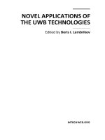
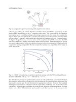
Fig. 6. The capacities of M-ary PSM, M-ary BPSM and M-ary OPPM-BPSM schemes in a
multipath environment where M=4 and 8.
−5 0 5 10 15 20 25 30
0
0.5
1
1.5
2
2.5
3
3.5
4
4.5
5
Eb/N0
bits/channel use
Capacity of 16−ary scheme in multipath environments
16−ary OPPM−BPSM(2 positions, 4 pulses)
16−ary OPPM−BPSM( 4 positions, 2 pulses)
16−ary BPSM
16−ary PSM
Fig. 7. The capacities of 16-ary PSM, 16-ary BPSM and 16-ary OPPM-BPSM schemes in
multipath environment.
47
Orthogonal Pulse-Based Modulation Schemes for Time Hopping Ultra Wideband Radio Systems
18 Name of the Book
we have used 1st order PSWF and 1st order MHP in 32-ary BPPM. It is known that both the
pules provide exactly the same correlation properties for the 1st order pulse. Fig. 6, Fig. 7 and
Fig. 8 show that the average full capacity for all values of M for M-ary PSM is nearly achieved
where the SNR is close to 23 dB, 20 dB for M-ary BPSM and 17 dB for M-ary OPPM-BPSM.
It is also observed that M-ary OPPM-BPSM has 3 dB more SNR than M-ary BPSM and 6 dB
greater SNR than M-ary PSM at the same capacity. This is because of the use of orthogonal
pulses resulting in that ISI and MAI are less for M-ary OPPM-BPSM scheme than M-ary PSM
and M-ary BPSM schemes for the same value of M. However, after 25 dB SNR, the capacities
are close to the same irrespective of the modulation schemes.
Under the same simulation condition the system capacities of 16-ary BPPM, 16-ary PSM,
16-ary BPSM and 16-ary OPPM-BPSM as a function of number of MPC are provided in
Fig. 9. It has been observed that capacities for all schemes decrease with increase in the
number of MPC. This is because ISI and MAI increase with the increase in the number of
MPC, resulting in the reduction of mutual information. It proves that mutual information is
inversely proportional to number of MPC. It is also observed that BPPM and OPPM-BPSM are
more sensitive to the number of MPC. When number of MPC is more than 10, the capacities of
BPPM and OPPM-BPSM are decreased more gradually than the PSM and BPSM scheme. It is
because of involving pulse position modulation in both BPPM and OPPM-BPSM. Indeed, it is
known that pulse position modulation is more sensitive in multipath environment. However,
OPPM-BPSM still outperforms conventional BPPM scheme for the same values of M.
5. Power spectral analysis of TH-UWB systems
In orthogonal pulse based signal, different symbols are transmitted by different order
orthogonal pulses. The continuous spectrum, energy spectral density (ESD), changes with
symbol. The discrete spectral component changes with orthogonality of the pulses and TH
code. Therefore, a mathematical frame work is essential to understand the orthogonal pulse
based PSD in the presence of deterministic TH code Majhi et al. (2010). We assume that
the analysis is only for 1 user. For simplicity, the superscript/subscript terms in (35) are
omitted/modified. After some modification, sum of M symbol can be written from (2) as
s
p
(t)=
M −1
∑
l=0
N
s
−1
∑
h=0
a
l
w
l
(t − lN
p
T
f
+ hT
f
−c
l,h
T
c
−δ
l
) (35)
where a
l
is the amplitude and δ
l
is the pulse position. The terms a
l
, δ
l
and w
l
are independent
and stationary process. The index p is related to TH code, c
l,h
,andTHperiod,N
p
. To simplify
the analysis of the PSD of TH-UWB signal, it is assumed that the number of time frames for a
symbol is N
s
and it is equal to N
p
. Since (35) depends on the time dithering, it can be written
in continuous form as
y
(t)=
∑
l
s
p
(t −lN
p
T
f
). (36)
The PSD is computed by evaluating the Fourier transform (FT) of the autocorrelation function
of y
(t) i.e.
P
y
( f )=F
E
{
y(t)y(t + τ)
}
(37)
48
Novel Applications of the UWB Technologies
Orthogonal Pulse-Based Modulation Schemes for Time Hopping Ultra Wideband Radio Systems 19
−5 0 5 10 15 20 25 30
0
0.5
1
1.5
2
2.5
3
3.5
4
4.5
5
Eb/N0
bits/channel use
Capacity of 32−ary scheme for PSWFs & MHPs
32−ary OPPM−BPSM (8 positions, 2 pulses)
32−ary OPPM−BPSM (2 positions, 8 pulses)
32−ary BPSM
32−ary PSM
32−ary BPPM
PSWFs
MHPs
Fig. 8. The capacity of 32-ary PSM, 32-ary BPSM and 32-ary OPPM-BPSM schemes schemes
in a multipath environment with different sets of orthogonal pulse waveforms.
10
0
10
1
10
2
0
0.5
1
1.5
2
2.5
3
3.5
4
Number of multipath components
Capacity bits/channel use
Capacity vs multipath component
16−ary OPPM−BPSM
16−ary BPSM
16−ary PSM
16−ary BPPM
Fig. 9. The capacity versus multipath components is provided for 16-ary BPPM, 16-ary PSM,
16-ary BPSM and 16-ary OPPM-BPSM schemes.
49
Orthogonal Pulse-Based Modulation Schemes for Time Hopping Ultra Wideband Radio Systems
20 Name of the Book
where F{.} denotes the FT and E{.} denotes the expectation operator. Therefore, the PSD can
be expressed as Padgett et al. (2003)
P
y
( f )=
1
N
p
T
f
E
|S
p
( f )|
2
− E
S
p
( f )S
∗
q
( f )
+
1
(N
p
T
f
)
2
∑
k
E
S
p
( f )S
∗
q
( f )
δ
f
−
k
N
p
T
f
(38)
where p and q are two independent random variables with the same probability distribution
function. S
p
( f ) is the FT of s
p
(t). It can be expressed as
S
p
( f )=
M −1
∑
l=0
W
l
( f )T
l
( f )a
l
e
−j2π f δ
l
(39)
where W
l
( f ) is the FT of the transmitted pulse w
l
(t). The time domain representation of
(l + 2)
th
order MHPs can be expressed as
nw
l+2
(t)=2tw
l+1
(t) −2(l + 1)w
l
(t) (40)
The FT of w
l+1
( f ) can be expressed as
W
l+1
( f )=j
1
4π
˙
W
l
( f ) −2π fW
l
( f )
(41)
where “ ˙” stands for derivative with respect to frequency. For MHP, W
0
( f ) is defined as
W
0
( f )=2
√
πe
−4π
2
f
2
(42)
The time and frequency domain representation of MHPs are given in Fig. 1.
T
l
( f ) is the FT of the TH code which transmits the l
th
symbol
T
l
( f )=
N
s
−1
∑
h=0
e
−j2π f
(
c
l,h
T
c
+(lN
p
+h)T
f
)
. (43)
To find the closed form expression of P
y
( f ) in (38), the expectation of |S
p
( f )|
2
is to be
evaluated. It is given as
E
|S
p
( f )|
2
=E
M −1
∑
l=0
M
−1
∑
n=0
W
l
( f )W
n
( f )
∗
T
l
( f )
×
T
n
( f )
∗
a
l
a
n
e
−j2π f
(
δ
l
−δ
n
)
.
(44)
Since a
l
and a
n
are independent random variables derived from the same process and δ
l
and
δ
n
are independent random variables derived from different processes. Therefore, (44) can be
50
Novel Applications of the UWB Technologies
Orthogonal Pulse-Based Modulation Schemes for Time Hopping Ultra Wideband Radio Systems 21
rewritten as
E
|S
p
( f )|
2
=
M −1
∑
l=0
|W
l
( f )|
2
|T
l
( f )|
2
E{a
2
l
}+
M −1
∑
n=0
n
=l
W
l
( f )W
∗
n
( f )T
l
( f )T
∗
n
( f )
×
E{a
l
}E{a
n
}E{e
−j2π f (δ
l
−δ
n
)
}
.
(45)
Similarly, the second expectation in (38) can be expressed as
E
{S
p
( f )S
∗
q
( f )}=
M −1
∑
l=0
M
−1
∑
n=0
W
l
( f )W
∗
n
( f )T
l
( f )T
∗
n
( f )
×
E
{
a
l
}E{a
n
}
E
e
−j2π f
(
δ
l
−δ
n
)
.
(46)
The waveforms s
p
(t) and s
q
(t) are generated by two i.i.d processes. Therefore, the expectation
in (46) is independent of l and n and equal to the case l
= n of (45) i.e.
E
{S
p
( f )S
∗
q
( f )} = E{a
l
}E{a
n
}E{e
−j2π f (δ
l
−δ
n
)
}
×
M −1
∑
l=0
M
−1
∑
n=0
W
l
( f )W
∗
n
( f )T
l
( f )T
∗
n
( f )
(47)
Substituting (45) and (47) in (38), the final PSD can be formulated as in (48)
P
y
( f )=
E{a
2
l
}−E{a
l
}E{a
n
}E{e
−j2π f (δ
l
−δ
n
)
}
N
p
T
f
M
−1
∑
l=0
|W
l
( f )|
2
|T
l
( f )|
2
+
E{a
l
}E{a
n
}E{e
−j2π f (δ
l
−δ
n
)
}
(N
p
T
f
)
2
M
−1
∑
l=0
M
−1
∑
n=0
W
l
( f )W
∗
n
( f )T
l
( f )T
∗
n
( f )
∑
k
δ
f −
k
N
p
T
f
(48)
Although UWB signals are alike in the frequency domain, they are diverse in the time domain
due to their different characteristics of time domain parameters N
p
, T
f
, a
l
and w
l
. We see that
the PSD of orthogonal pulse-based modulation signals consists of continuous and discrete
spectral components which change with the order of pulse waveforms and modulation
schemes. The variation of PSD over different orthogonal pulse-based signaling are given in
the following section.
5.1 PSD of M-ary PSM scheme
In PSM scheme, symbols are modulated only by the order of orthogonal pulses. The
generalized terms in (48) are specified by a
l
=1 and δ
l
= 0. The expectations of these variables
are E
{a
2
l
} = 1, E{a
l
}E{a
n
}
l=n
= 0andE{e
−j2π f (δ
l
−δ
n
)
} = 1 respectively. The PSD of the
PSM signal can be written from (48) as
P
y
( f )=p( f )+p
k
( f ) (49)
51
Orthogonal Pulse-Based Modulation Schemes for Time Hopping Ultra Wideband Radio Systems
22 Name of the Book
where
p
( f )=
1
N
p
T
f
M
−1
∑
l=0
|W
l
( f )|
2
|T
l
( f )|
2
(50)
and
p
k
( f )=
1
(N
p
T
f
)
2
M
−1
∑
l=0
M
−1
∑
n=0
W
l
( f )W
∗
n
( f )T
l
( f )T
∗
n
( f )
×
∑
k
δ
f −
k
N
p
T
f
(51)
We see that p
( f ) is continuous spectrum component. It depends on the TH code and the
ESD of the l
th
order orthogonal pulse. Since ESD of different order orthogonal pulses are not
identical, the selection of order of the orthogonal pulses plays an important role for continuous
spectral component.
p
k
( f ) is the discrete spectral component which induces UWB interference on the other narrow
band systems Majhi, Madhukumar & Ye (2007). The discrete components of the signal appear
based on the term
∑
k
δ
f −
k
N
p
T
f
. It shows that the position of discrete component depends
on the TH code and its dynamic range of amplitude depends on the orthogonality of pulses.
Since pulses are orthogonal in time and frequency domains, the value of W
l
( f )W
∗
n
( f ) is
approximately zero, as a result, the dynamic range of amplitude of the discrete spectral
components becomes very small. This small dynamic range increases the average transmitted
power in pulse and improves the UWB system performance. It helps UWB signal to coexist
with other systems without any serious performance degradation. In addition, it facilitates
UWB signal to keep its spectrum under the FCC spectral mask without minimizing the
average transmitted power in the signal.
5.2 PSD of M-ary BPSM scheme
In BPSM scheme, symbols are modulated by order and amplitude of the pulses, i.e. a
l
∈
{±1} and δ
l
= 0. The expectation of these variables are E{a
2
l
} = 1, E{a
l
}E{a
n
}
l=n
= 0and
E
{e
−j2π f (δ
l
−δ
n
)
} = 1. The corresponding PSD of BPSM scheme can be expressed from (48) as
P
y
( f )=
1
N
p
T
f
M
−1
∑
l=0
N
s
−1
∑
h=0
N
s
−1
∑
k=0
|W
l
( f )|
2
×exp
−j2π f
(c
l,h
−c
l,k
)T
c
+(h −k)T
f
(52)
The continuous PSD component of BPSM signal is same as PSM scheme. However, the
discrete spectral components become zero due to the antipodal pulse. The PSD of the
TH-UWB signal for BPSM scheme is smoothed. This allows the signal to coexist with other NB
signals. The extensive studies found that any antipodal signal has only continuous spectral
component Majhi, Madhukumar & Ye (2007). The continuous component can be easily fitted
to FCC by using appropriate MHPs.
52
Novel Applications of the UWB Technologies
Orthogonal Pulse-Based Modulation Schemes for Time Hopping Ultra Wideband Radio Systems 23
0 2 4 6 8 10 12
x 10
9
−90
−80
−70
−60
−50
−40
−30
Frequency [Hz]
PSD in dBm/MHz
FCC
PSD
8 8.5 9
x 10
9
−58
−57
−56
−55
−54
−53
−52
Amplitude of
dynamic
range
=8 dB
Fig. 10. PSD of 8-ary OPPM scheme with 3
rd
order MHP and TH code length is 8.
5.3 PSD of M-ary OPPM-BPSM scheme
For OPPM-BPSM scheme, a
l
∈{±1} and δ
l
=(l − 1)δ,whereδ is the constant time shift
length. This implies, E
{a
2
l
} = 1, E{a
l
a
n
} = 0andE{e
−j2π fmT
Δ
δ
} =(1 + cos(2πmfT
Δ
))/2.
The corresponding PSD of OPPM-BPSM signal can be expressed as
P
y
( f )=
1
N
p
T
f
M
−1
∑
l=0
N
s
−1
∑
h=0
N
s
−1
∑
k=0
|W
l
( f )|
2
×exp
−j2π f
(c
l,h
−c
l,k
)T
c
+(h −k)T
f
(53)
The PSDs of BPSM and OPPM-BPSM schemes are identical. However, OPPM-BPSM can
be used for higher level modulation scheme for higher data rate systems. Therefore,
OPPM-BPSM modulation is an attractive choice of TH-UWB signal from several aspects.
6. Simulation results and discussions
In this section, PSD is provided for orthogonal pulse-based signaling and compared with
conventional OPPM scheme. In simulation, different order of MHPs are used with two
different lengths of TH code 8 and 16. The other simulation parameters are set to T
f
= 60
ns and pulse width is 0.7ns.
Since BPSM and OPPM-BPSM have antipodal signal, they have only continuous spectral
component and shape of their spectral is same as continuous component of non antipodal
signal. The only difference is that spectral of antipodal signal does not contain any discrete
component. The PSD in non antipodal modulation schemes is more complicated. Since OPPM
and OPPM-PSM are special cases of OPPM-BPSM, OPPM and OPPM-PSM have been chosen
53
Orthogonal Pulse-Based Modulation Schemes for Time Hopping Ultra Wideband Radio Systems
24 Name of the Book
0 2 4 6 8 10 12
x 10
9
−90
−80
−70
−60
−50
−40
−30
Frequency [Hz]
PSD in dBm/MHz
0 2 4 6 8 10 12
x 10
9
−90
−80
−70
−60
−50
−40
−30
Frequency [Hz]
PSD in dBm/MHz
FCC
PCD
FCC
PCD
Fig. 11. (a) PSD of 8-ary OPPM scheme with 4
th
order MHP. (b) PSD of 8-ary OPPM scheme
with 5
th
order MHP and TH code length is 8
to compare the PSD of the signal. The PSD of 8-ary OPPM is given in Fig.10 for 3
rd
order
pulse and in Fig.11 for 4
th
and 5
th
order pulses with TH code of length 8 and T
c
= 7.5ns.Since
each time only one pulse is used in OPPM scheme, orthogonality is maintained by position
not by pulse. The 3
rd
order pulse almost satisfy the FCC spectral mask except some discrete
components. However, 4
th
and 5
th
order pulses do not satisfy the FCC spectral mask shown
in Fig.11. The dynamic range of the amplitude of discrete components of OPPM scheme is
about 8 dB which is very high. The power of the signal is calculated based on the line where
the dynamic range is zero (4 dB below from the pick point). As FCC rules, pick amplitude
must be below the -41.25 dBm limit. Therefore, the power of the signal is calculated based
on the line which is maximum up to -45.25 dBm. As a result, signal provides low average
transmitted power which degrades the system performance. Not that if the dynamic range
becomes zero, the maximum limit becomes -41.25 dBm.
Fig. 12 shows the PSD of 8-ary OPPM-PSM for 4 positions and 2 orthogonal pulses with TH
code of length 8. We see that that dynamic range of the amplitude of the discrete spectral
component of OPPM-PSM scheme is 4 dB which is lower than the OPPM scheme even
the same length of TH code is used. It is because of the orthogonality of pulses. So by
reducing dynamic range, we can improve the UWB system performance by increasing the
average transmitted power in the signal pulse as well as we can reduce the UWB interference
over other radio systems. Again by applying TH code over these orthogonal pulse-based
modulation, dynamic range of amplitude of discrete component further could be reduced.
Fig. 13 shows the PSD of 8-ary OPPM-PSM with TH code of length 16 and T
c
= 3.75ns.The
dynamic range is almost reduced to 1 dB. However, it can not be reduced to zero whatever
the length of TH code used. We also see that the average transmitted power in Fig. 13 is more
54
Novel Applications of the UWB Technologies
Orthogonal Pulse-Based Modulation Schemes for Time Hopping Ultra Wideband Radio Systems 25
0 2 4 6 8 10 12
x 10
9
−90
−80
−70
−60
−50
−40
−30
Frequency [Hz]
PSD in dBm/MHz
FCC
PSD
Amplitude of
dynamic
range
=4 dB
Fig. 12. PSD of 8-ary OPPM-PSM schemes for 4 positions and 2 pulses (0
th
and 3
rd
)withTH
code of length 8
0 2 4 6 8 10 12
x 10
9
−90
−80
−70
−60
−50
−40
−30
Frequency [Hz]
PSD in dBm/MHz
FCC
PSD
5.6 5.8 6 6.2
x 10
9
−44
−43
−42
−41
Fig. 13. PSD of 8-ary OPPM-PSM schemes for 4 positions and 2 pulses 0
th
and 3
rd
with TH
code of length 16
55
Orthogonal Pulse-Based Modulation Schemes for Time Hopping Ultra Wideband Radio Systems
26 Name of the Book
than the previous cases. Therefore, orthogonal pulse-based TH-UWB signaling has several
advantages than its complexity burden.
7. Summary
This book chapter provides TH-UWB system model based on orthogonal pulse waveform
such as MHPs and PSWFs. The performance of orthogonal pulse based modulation schemes
is provided over multipath channel. Several interference issues such as ISI and MAI are
provided in the presence of RAKE reception. The system capacity of pulse based modulation
schemes over multipath channel is analyzed in details. Finally PSD analysis for PSM, BPSM
and OPPM-BPS is drawn by using two different sets of orthogonal pulse waveforms.
8. References
(n.d.).
Benedetto, M. G. D. & Giancola, G. (2004). Understanding Ultra Wideband radio fundamentals,
Prentice Hall.
Bin, L., Gunawan, E. & Look, L. C. (2003). On the BER performance of TH-PPM UWB using
Paa’s monocycle in the AWGN channel, IEEE Conference on Ultra Wideband Systems
and Technologies, pp. 403–407.
Chu, X. & Murch, R. (2005). Multidimensional modulation for ultra-wideband multiple-access
impulse radio in wireless multipath channels, IEEE Transaction on Wireless
Communication 4: 2373–2386.
de Abrue, G. T. F. & Kohno, R. (2003). Design of jitter-robust orthogonal pulse-shape
modulation for UWB systems, IEEE Global Telecommunication Conference, pp. 739–743.
de Abrue, G. T. F., Mitchell, G. T. & Kohno, R. (2003). On the design of orthogonal pulse-shape
modulation for UWB systems using Hermite pulses, Journal Of Communications And
Networks 5: 328–343.
Dilmaghani, R. S., Ghavami, M., Allen, B. & Aghvami, H. (2003). Novel UWB pulse shaping
using Prolate spheroidal wave functions, The 14th IEEE International Symposium on
Personal, Indoor and Mobile Radio Communication Proceedings, pp. 602 – 606.
Durisi, G. & Benedetto, S. (2003). A general method for SER computation of M-PAM
and M-PPM UWB systems for indoor multiuser communications, IEEE Global
Telecommunication Conference, pp. 734–738.
Foerster, J. (2003). UWB channel modeling sub-committee report final, IEEEP802.15 Working
Group for Wireless Personal Area Networks (WPANs) .
Gezici, S. & Kobayashi, H. (2005). Performance evaluation of impulse radio UWB systems
with pulse-based polarity randomization, IEEE Transactions on Signal Processing,
pp. 2537–2549.
Gezici, S., Sahinoglu, Z., kobayashi, H. & Poor, H. V. (2006). Ultra-wideband impulse radio
systems with multiple pulse types, IEEE Journal n Selected Areas in Communications
24: 892–898.
Ghavami, M., Michael, L. B., Haruyama, S. & Kohno, R. (2002). A novel UWB pulse shape
modulation system, Wireless Personal Communications 23: 105–120.
Giorgetti, A. & Chiani, M. (2005). Influence of fading on the Gaussian approximation for BPSK
and QPSK with asynchronous cochanel interference, IEEE Transaction on Wireless
Communications 4.
56
Novel Applications of the UWB Technologies
Orthogonal Pulse-Based Modulation Schemes for Time Hopping Ultra Wideband Radio Systems 27
Guvenc, I. & Arslan, H. (2003). On the modulation option for UWB systems, IEEE Military
Communications Conference, pp. 892–897.
Harada, H., Ikemoto, K. & Kohno, R. (2004). Modulation and hopping using modified
Hermite pulses for UWB communication, IEEE Conference on Ultra Wideband Systems
and Technologies, pp. 336–340.
Hu, B. & Beaulieu, N. C. (2004). Pulse shaping in UWB communications systems, IEEE
Vehicular Technology Conference, pp. 5175– 5179.
Hu, W. & Zheng, G. (2005). Orthogonal Hermite pulses used for UWB M-ary communication,
Proceeding of the International conference on Information Technology, pp. 97–101.
Hwang, J. H., Kim, S. C., S. Yoon, B. K. & Park, J. S. (2007). Performance analysis of PO-THMA
UWB system using mutually orthogonal MHP pulses, IEEE Transactions on Consumer
Electronics 53.
Jia, T. & Kim, D. I. (2005). Analysis of average signal-to-interference-noise ratio for indoor
UWB rake receiving system, in proceedings of IEEE 61st Vehicular Technology Conference,
pp. 1396–1400.
Jiang, L., , Wang, Y. & Guo, J. (2005). The capacity of M-ary PPM ultra-wideband
communication over multipath channels, IEEE International Symposium on Microwave,
Antenna, Propagation and EMC Technology for Wireless Communication Proceedings,
pp. 1606–1609.
Kim, Y., Jang, B., Shin, C. & Womack, F. (2005). Orthonormal pulses for high data rate
communication in indoor UWB systems, IEEE Communication Letters 9: 405–407.
Kim, Y. & Womack, B. F. (2007). Performance evaluation of UWB systems exploiting
orthonormal pulses, IEEE Transactions on Communication 55.
Li, W., Gulliver, T. A. & Zhang, H. (2005). Performance and capacity of ultra-wideband
transmission with pulse position amplitude modulation over multipath fading
channels, IEEE Global Telecommunications C onference, pp. 225–229.
Majhi, S., Madhukumar, A. S., Nasser, Y. & Hélard, J F. (2010). Power spectral analysis of
orthogonal pulse-based th-uwb signals, VTC Spring, pp. 1–5.
Majhi, S., Madhukumar, A. S. & Premkumar, A. B. (2006). Reduction of UWB interference
at NB systems based on a generalized pulse waveform, IEICE Electronics Express
3: 361–367.
Majhi, S., Madhukumar, A. S. & Premkumar, A. B. (2007). Performance of orthogonal based
modulation schemes for TH-UWB communication systems, IEICE Electronics Express
4: 238–244.
Majhi, S., Madhukumar, A. S., Premkumar, A. B. & Chin, F. (2007a). M-ary signaling for ultra
wideband communication systems based on pulse position and orthogonal pulse
shape modulation, IEEE Wireless Communication and Networking Conference (WCNC),
pp. 2795 – 2799.
Majhi, S., Madhukumar, A. S., Premkumar, A. B. & Chin, F. (2007b). Modulation schemes
based on orthogonal pulses for time hopping ultra wideband radio systems, IEEE
International Conference on Communications (ICC), pp. 4185–4190.
Majhi, S., Madhukumar, A. S., Premkumar, A. B. & Richardson, P. (2008). Combining OOK
with PSM modulation for simple transceiver of orthogonal pulse-based TH-UWB
systems, EURASIP Journal on Wireless Communications and Networking 2008: 11.
Majhi, S., Madhukumar, A. S., Premkumar, A. B., Xiang, W. & Richardson, P. (2011). Enhancing
data rates of TH-UWB systems using M-ary OPPM-BPSM modulation scheme: A
system perspective, Wireless Personal Communications 56: 583–597.
57
Orthogonal Pulse-Based Modulation Schemes for Time Hopping Ultra Wideband Radio Systems
28 Name of the Book
Majhi, S., Madhukumar, A. S. & Ye, Z. (2007). Coexisting narrowband and ultra wideband
systems: Analysis of power spectral density and in-band interference power, World
Scientific and Engineering Academy and Society (WSEAS) 6: 318–324.
Majhi, S., Xiang, W., Madhukumar, A. S. & Premkumar, A. B. (2008). Theoretical capacity
analysis of th-uwb systems for orthogonal pulse based modulation schemes, VTC
Fall, pp. 1–5.
Michell, C., de Abreu, G. T. F. & Kohno, R. (2003). Combined pulse shape and pulse position
modulation for high data rate transmission in ultra-wideband communication,
International Journal of Wireless Information Networks 10: 167–178.
Mitchell, C. J. & Kohno, R. (2004). Orthogonality and coded modulation for combined pulse
position and pulse shape modulation, International Workshop on UWB Systems, Joint
with Conference on UWB Systems and Technologies, pp. 177–181.
Padgett, J. E., Koshy, J. C. & Triolo, A. A. (2003). Physical-layer modeling of UWB interference,
White Paper of Telcordia Technologies pp. 1–121.
Parr, B., Cho, B., Wallace, K. & Ding, Z. (2003). A novel ultra-wideband pulse design
algorithm, IEEE Communication Letters 7.
Proakis, J. G. (2001). Digital Communications, New York, NY, McGraw-Hill inc., Fourth Edition.
Ramseier, S. & Schlegel, G. (1993). Bandwidth power efficiencies of trellis coded modulation
schemes, IEEE GLOBAL Telecommunicaiton Conference, pp. 1634–1638.
Saleh, A. & Valenzuela, R. (1987). A statistical model for indoor multipath propagation, IEEE
Journal of Selected Area in Communication 5: 128–137.
Sklar, B. (2001). Digital Communications Fundamentals and Applications,Singapore,Pearson
Education, Second Edition.
Usuda, K., Zhang, H. & Nakagawa, M. (2004). M-ary pulse shape modulation for PSWF-based
UWB systems in multipath fading environment, IEEE Global Telecommunication
Conference, pp. 3498–3504.
Wen, H. & Guoxin, Z. (2005). Orthogonal hermite pulses used for UWB M-ary communication,
Proceedings of the International Conference on Information Technology, pp. 97–101.
Win, M. Z. & Scholtz, R. A. (1998a). Impulse radio: How it works, IEEE Communication Letters
2: 36 – 38.
Win, M. Z. & Scholtz, R. A. (1998b). On the energy capture of ultrawide bandwidth signals in
dencemultipath environment, IEEE Communication Letters 2: 245 – 247.
Zhang, H. & Gulliver, T. (2005a). Biorthogonal pulse position modulation for time-hopping
multiple access UWB communications, IEEE Transaction on Wireless Communication
4: 1154–1162.
Zhang, H. & Gulliver, T. A. (2005b). Performance and capacity of PAM and PPM UWB
time-hopping multiple access communications with receive diversity, EURASIP
Journal on Applied Signal Processing 2005: 306–315.
Zhang, L. & Zhou, Z. (2005). Research on orthogonal wavelet synthesized UWB waveform
signal, IEEE International Conference on Communication, pp. 803–805.
58
Novel Applications of the UWB Technologies
3
A 0.13um CMOS 6-9GHz 9-Bands Double-Carrier
OFDM Transceiver for Ultra Wideband
Applications
Li Wei, Chen Yunfeng, Gao Ting, Zhou Feng, Chen Danfeng,
Fu Haipeng and Cai Deyun
State Key Laboratory of ASIC & System, Fudan University
China
1. Introduction
Since 2002, ultra wideband (UWB) technology has ignited the interests of academia and
industry for its potential of achieving high-speed wireless communication in short distance
with low power. It is actively investigated today due to the wide available bandwidth for
very high data rate up to 480Mb/s and low power service over short distances in 10m range.
According to FCC (Federal Communications Commission), the frequency spectrum
allocated for UWB is 3.1-10.6 GHz, and the spectrum shape of modulated output power and
maximum power level are limited to -41.3dBm/MHz, which ensures that UWB can coexist
with existing spectrum users like GSM(Global System of Mobile communication),
WLAN(Wireless Local Area Network) and Bluetooth.
Based on MB-OFDM(Multi-Band Orthogonal Frequency Division Multiplexing), WiMedia
released the initial version of Physical Layer (PHY) Specification in September 2005. In this
proposal, the UWB frequency spectrum from 3.1 GHz to 10.6 GHz is divided into 14
channels with 528MHz for each channel. These sub-bands are grouped into five band
groups. It is seen that by increasing the signal bandwidth significantly, ultra-wideband
achieves a high channel capacity and becomes an attractive solution to the ever-increasing
data rate demands in wireless personal area networks (WPAN). In December 2005,
European Computer Manufacturer's Association (ECMA) proposed the standard ECMA
368/369 on high-speed UWB physics layer and media access control layer based on MB-
OFDM scheme. This has pushed the industrialization of UWB technology to a new stage
again.
In China, UWB technology has also become a hot topic according to the issue of the UWB
standard by Chinese Government in 2008. A new UWB scheme named dual carrier-
orthogonal frequency division multiplexing (DC-OFDM ) has been proposed and applied in
China. In China standard, only the band from 6.2GHz to 9.4GHz and the band from 4.2GHz
to 4.8GHz are available for UWB applications. These bands are partitioned into 14 sub-
bands of 264MHz bandwidth which means the bandwidth is halved in China’s DC-OFDM
standard compared with the ECMA 368/369 standard. Thus the sampling frequency of the
DACs(Digital-to-Analog Converter) and ADCs(Analog-to-Digital Converter) are halved too.
The power consumption of the system can be reduced greatly. Moreover, in DC-OFDM
Novel Applications of the UWB Technologies
60
UWB, two bands locating around two different carriers are utilized at the same time to form
a bandwidth of 528 MHz for maintaining high-speed communication. In this way, the
spectrum usage is more flexible and the spectrum efficiency is enhanced. However, the
requirements of less than 9-ns hopping time of the carrier frequency as well as simultaneous
dual-carrier outputs challenge the design of dual-carrier frequency synthesizer. Fig.1 shows
the frequency spectrum for WiMedia and China UWB standard.
A fully integrated transceiver for DC-OFDM UWB system in the 6-9GHz band is present in
this chapter. This chapter will describe the realization of a DC-OFDM UWB transceiver
covering 6-9GHz bands in a low cost 0.13um CMOS process. Firstly, the RF receiver design
will be described in section 2. Section 3 and 4 introduce respectively the designs of the RF
transmitter and the 9-bands frequency synthesizer. The detailed measurement results are
demonstrated in section 5, which is followed by the conclusions in section 6.
4356
4620
6336 6600 6864 7392 7656 8184 8448
9240
7128 7920 8712
f(MHz)
8976
f(MHz)
4488 6336 6600 6864 7392 7656 8184 8448
9240
7128 7920 8712
8976
4356 4620
3
rd
group 4
th
group
2
nd
group 3
rd
group 4
th
group
5
th
group
1
st
group
WiMedia Frequency Bands
China UWB Standard Frequency Plan
Fig. 1. Frequency spectrum for WiMedia and China UWB standard
2. RF receiver design
Fig.2 shows a block diagram of the proposed UWB receiver. Signals are received and filtered
by the off-chip antenna and the RF(Radio Frequency) filter firstly. And then the received
signals are amplified and converted to IF(Inter-media Frequency) baseband signal by RF
front-end building blocks. After further filtering and amplifying, the analog baseband
signals should be large enough to drive the ADC for digital signal processing. The receiver's
local oscillator (LO) should be a fast-hopping frequency synthesizer that generates carrier
tones according to the band plan in Fig.1. Performances such as in-band phase noise and
reference spur are specified as -80 dBc and -40dBc respectively, which are not so stringent.
And the I/Q mismatch is designed as 2.5 degree and 0.2 dB.
Normally the noise figure of channel select filter is around 30 dB, thus the conversion gain
of RF front-end building blocks should be larger than 30 dB to suppress the noise from
LPF(Low Pass Filter). But in that case, the linearity of the receiver will get worse. In order to
improve the linearity of the receiver, the conversion gain of the RF front-end building blocks
is set to be around 24 dB(average) with variable gain of 12 dB. The NF(Noise Figure) of the
LPF is designed to be less than 18 dB to guarantee low noise of the receiver. The LNA(Low
Noise Amplifier) utilizes a fully differential structure and presents an input matching to
A 0.13um CMOS 6-9GHz 9-Bands
Double-Carrier OFDM Transceiver for Ultra Wideband Applications
61
50ohm for the off-chip antenna. It should provide a maximum gain of 18 dB to suppress
noise from mixer and baseband circuits. As LNA sets the baseline for the noise figure of the
receiver, the NF of the LNA should be optimized to lower than 5 dB. Following is a
quadrature mixer with a fixed gain of 6 dB. The 5th-order Chebyshev type band-selection
LPF is implemented after the mixer. Unlike normal channel select filter, the proposed LPF
should provide a maximum gain of 30 dB, with a NF less than 18 dB at maximum gain
mode.
According to the Friis Equation, the noise of the LPF nearly doesn't contribute to the total
input referred noise of the receiver, leading to a very low noise figure. As the back-end block
of the receiver, the filter tackles with slightly large signals, leading to stringent linearity
requirement for the filter. Since the filter suppresses adjacent channel interferers to some
extent, the linearity of the filter is proportionally improved. Sharp rejection of out-of-band
signal is also required. Considering the difference between the sub-band's bandwidth of two
standards, the cut-off frequency of the filter is switchable between 264 MHz and 132 MHz.
Finally, the PGA(Programmable Gain Amplifier) amplifies the signal from the LPF and
delivers constant-magnitude signals to the ADC.
I&Q
LO
I
Q
132/264MHz Analog Baseband
6.2-9.5GHz RF
front-end
Off chip antenna and
RF filter
Digital
Control
To 6bit
ADC
LNA
Fig. 2. Architecture of the proposed receiver
2.1 RF front-end design
Attaining an input impedance match for the wide band receiver is particularly difficult
because parasitic may dominant the input impedance network. Fig.3 gives a presentation of
the LNA for the proposed UWB receiver. A resistive shunt feedback topology is adopted in
the LNA design, which achieves a wideband matching with a good balance between area
cost and performances. Although there is a slight degradation of the noise figure comparing
to other techniques like LC ladder (Bevilacqua A. et al., 2004) and transformer feedback
matching (Shin D. H., et al., 2007), quite a large number of inductor coils are avoided.
Bonding wire inductance L
bonding
and the ESD(Electro-Static Discharge) capacitance together
with the PAD capacitance C
pad
are co-designed with other on-chip components. The load
stage is an R-L-C tank. The load inductor LL can be replaced by a differential inductor to get
a smaller area. However, we split it into two symmetrical inductors for convenience of
cascading with mixer in the layout. A fully differential topology is utilized in LNA design to
have the input impedance match independent of the bonding wire inductance from the
source of M1 to ground. Fig.4 shows the simulated S11 with different bonding wire
inductance.
Novel Applications of the UWB Technologies
62
L
R
L
L
L
L
in
V+
in
V-
f
R
f
R
f
C
f
C
2
M
2
M
1
M
1
M
Fig. 3. Schematic Diagram of Low Noise Amplifier
5 6 7 8 9 10
-30
-25
-20
-15
-10
-5
0
Frequency(GHz)
Input Return Loss (S11)(dB)
1.8nH
2.2nH
2nH
Fig. 4. Simulated S11 with different bonding wire inductance
A 0.13um CMOS 6-9GHz 9-Bands
Double-Carrier OFDM Transceiver for Ultra Wideband Applications
63
Fig.5 shows the folded quadarture down- conversion mixer for the UWB receiver. A fully
differential Gilbert-cell based structure with I/Q branches sharing the same RF input stage
is implemented in the mixer, which eliminates the mismatch present in down conversion
topology with separate I/Q mixers. Exploring merged architecture (Sjöland H, et al., 2003)
for the quadrature mixer can also minimize the capacitive load to the LNA. Compared with
the traditional structure of mixer, the folded structure utilized in this work separates the
input stage and switching stage. Thus different bias current can be applied to the input stage
and switching stage, better performances are achieved. The bias current of the input stage is
bigger to guarantee good performance on conversion gain and noise figure. On the contrary,
small current in the switching stage can lower the 1/f noise and dc-offset, which is
significantly important in zero-IF receivers.
M
R
M
R
M
R
M
R
M
L
Fig. 5. Quadrature down conversion mixer circuit
2.2 Analog base-band design
The main difference between the two standards is that the intermediate frequency is
4.125MHz-264MHz and 1MHz-132MHz for WiMedia MB-OFDM and China UWB standard
respectively. In order to support both standards, the cut-off frequency of the band-select
filter should be switchable between 132MHz and 264MHz. Using two different filters to
support each standard may be a possible solution, but will sacrifice a lot of die area.
Furthermore, as the first stage of IF stage, the NF and linearity of the filter should be
optimized. Thus the LPF should provide variable gain to suppress noise substantially at
maximum gain mode and meet the linearity requirement when set as minimum gain. In this
work, a fifth-order Chebyshev type programmable Gm-C filter is implemented.
The fifth order low pass filter is realized by a cascade of a first order RC filter and two
biquads. The proposed architectures of the low pass filter and the biquad are illustrated in
Fig.6. Note that the down-conversion mixer’s load resistors are utilized to form the first
passive RC filter stage. As a result, simulations covering both the mixer and the filters
should be taken to make sure that the overall frequency response and gain are optimized.
Novel Applications of the UWB Technologies
64
The modified Nauta Gm cell (as shown in Fig.7) is implemented as the OTA(Operational
Transconductance Amplifier) in the filter. The transconductances of the all the OTA are
controlled by the digital data.
5-bit DCCA
4
b
1
b
0
b
M
C
OTA1
OTA 3
OTA2
OTA 4
ip
v
in
v
op
v
on
v
C
C
C
C
5
b
OTA1
ip
v
in
v
OTA1
ip
v
in
v
5
b
5
b
5
b
Fig. 6. Structure of the Low Pass Filter
INV3
vout +
S
S
S
S
S
S
S
S
S
S
INV4
INV5
INV6
INV1
vout -
S
S
INV2
Fig. 7. Modified Nauta OTA
The topology of the PGA (Programmable Gain Amplifier) is based on a source degenerated
structure as illustrated in Fig.8. A switched resistor array is implemented to achieve variable
gain from 0dB to 18dB with 2dB/step. High-gain amplification easily causes the following
stages into saturation due to DC-offset and DC offset also leads to second-order harmonic
distortion (HD2) of the received signals, resulting in SNR(Signal-to-Noise Ratio)
degradation. Thus the DC-offset cancellation circuits are also included in the PGA design.
The amplitude response of the PGA is designed to be flatness within the frequency range of
264MHz.
A 0.13um CMOS 6-9GHz 9-Bands
Double-Carrier OFDM Transceiver for Ultra Wideband Applications
65
ip
V
in
V
1
M
1
M
op
V
on
V
L
R
S
R
Swithched Resistor Array
DCOC
Fig. 8. Topology of the PGA
3. RF transmitter design
The proposed transmitter utilizes the direct conversion architecture for its easiness of
integration and low cost. As shown in Fig.9, it consists of a dual-mode I/Q LPF with mode-
switch circuits, an I/Q up-conversion mixer with high-linear voltage-to-current (V2I) units,
a two-stage power driver amplifier (PA). Besides, the trans-impedance amplifiers (TIAs) are
integrated to measure the AC transfer character of the LPF.
The main signal flow of this transmitter is as follows. The ABB(Analog Baseband) voltage
signals from the DACs are applied at the inputs of the I/Q LPF. With the correct mode-
switch bit as well as the Digital Control Capacitor Array (DCCA) control word, the image
signals of the DACs and the unwanted high frequency spurs are all filtered out in both 264-
MHz and 132-MHz modes. After the output voltages of the LPF are converted into ABB
currents by V2I units, they are up-converted into RF voltages by the switches in the up-
conversion mixer at the rate of LO. Lastly, the differential RF voltages are amplified by
PA(Power Amplifier) and are converted into single-ended one via the 6-9 GHz off-chip
balun, to drive the antenna.
Fig. 9. Block diagram of the proposed transmitter
3.1 Dual-mode I/Q LPF design
The main requirements of this LPF are the attenuation of the out-band signals, the in-band
ripple, the dual-mode operation with accurate cut-off frequency controlling and
accommodation to the large input ABB voltages. According to the sampling rate of a
common UWB DAC, the LPF should have an attenuation of about 45 dB from 264/132 MHz
Novel Applications of the UWB Technologies
66
to 600/300 MHz at 264/132-MHz mode. Moreover, an in-band ripple of 0.5 dB is required.
To obtain comparably good phase linearity, the 5th-order Chebyshev gm-c LPF is proposed.
Besides, to deal with the ABB voltage as large as 300mVpp, the passive sub-filter is placed as
the 1st-stage and the high-Q biquad is as the last stage. Also, to improve the linearity of the
LPF under low supply voltage with low power, the trans-conductors are built with the
Nauta’s structure (Nauta B, et al., 1992).
Fig. 10. Architecture of the 5th-order Chebyshev LPF with mode-switch circuits
3.2 Up-conversion mixer design
The simplified I-path schematic of the up-mixer is shown in Fig.11. It utilizes two double
balanced Gilbert cells with their outputs summed to realize single-sideband (SSB) up-
mixing. Since the I/Q up-mixer acts as I/Q modulator and up-conversion mixer in direct
conversion transmitter, the performances of the transmitter are mainly determined by this
circuit.
Low spurs, high linearity and wide bandwidth are the main challenges for the design of this
up-conversion mixer. The main spurs in the output spectrum of the transmitter are the LO
leakage and the sideband signal. The power of the LO leakage is determined by the offset of
the I/Q ABB path. In order to reduce the power of LO leakage, an AC coupling is utilized
between the V2I unit and the switches of the up-mixer as shown in Fig. 11. Besides, the
linearity of the up-mixer is mainly affected by the V2I unit while the impact of the switch
stage is of less importance (Zheng Renliang, et al., 2009). Many techniques (Willy Sansen,
2006) have been proposed to improve the linearity of the V2I unit. Although the complete
OPAMP-assisted V2I possess better linearity, its application is restricted by the power
consumption to achieve sufficient GBW(Gain Bandwidth) of the OPAMP for UWB ABB as
well as the limited voltage swing because of the low supply voltage. Instead, the simple
OPAMP-assisted V2I unit is preferred. As shown in Fig.11, the V2I unit consists of the input
PMOS transistor M1, the source degeneration resistor R1, the current-mirror transistor M2,
M3, the AC coupling capacitor CB as well as the bias resistor for eliminating the DC-offset in
V2I. The feedback loop is composed of M1, R1, M2, I1 and I2, where M2 acts as the simple
single-transistor OPAMP. When applied at the gate of M1, the input ABB voltage is directed
transferred to the terminals of R1, because any voltage changes at the gate will be
transferred to the source of M1 to maintain a fixed V
GS
as required by the current source I1
and I2. Thus the input voltage is converted linearly into its current counterpart with a gain
of 1/R1. The converted current ∆i circulates in M2. Then it is mirrored into the up-mixer by
M3. A 400-Ω R1 is used to improve the linearity at the cost of the gain loss in V2I. To
A 0.13um CMOS 6-9GHz 9-Bands
Double-Carrier OFDM Transceiver for Ultra Wideband Applications
67
compensate it, a 6-dB gain is set at the current mirror. Furthermore, a broadband operation
of the mixer is achieved by employing a differential inductor Ld to peak with the parasitic
capacitance Cpar and two series resistors Rs to reduce Q of the overall load network.
2
3
2
(W/L)
(W/L)
Fig. 11. Simplified I-path schematic of the up-mixer and its wideband load network
3.3 Power driver amplifier
Since the PA is the last stage of the transmitting chain, its linearity determines the output
IP3(Input 3rd order Intercept Point) of the transmitter according to the Friis’ formula.
Moreover, the PA should possess sufficient gain to boost the output power of the up-mixer
as well as to reduce the impact of former stages on the linearity of the transmitter. A flat
gain of the PA is desired, too. Besides, considerations of the rejection to common-mode
interferences should be taken because the tail current sources are eliminated to fit the low
supply voltage.
As shown in Fig.12, the 1st stage of the PA is a combination of source follower (M1) and
common source (M2) amplifier (Chang-Wan Kim, et al., 2005). The phase shift of the signal
passing through the two amplifiers is 0°and 180°respectively. When the input signal Vin is
applied at the two amplifiers, the common-mode signals in Vin become out-of-phase and
their amplitudes are subtracted at node X/Y while the differential-mode signals in Vin
become in-phase and their amplitudes are added at node X/Y. In this configuration, the
input differential signals are amplified with the common-mode signals rejected. Therefore,
the 1st stage increases the common-mode rejection ratio (CMRR) of the transmitter. In order
to obtain a high CMRR, the gain of the two appliers, i.e. the source follower and the
common source amplifier, should be equal. The transistors M1 and M2 have the identical
size. Under this condition the ideal CMRR is infinite and the differential voltage gain is 6 dB.
However, the post simulation of this circuit indicates that the CMRR is improved by 12 dB
and the differential voltage gain is about +2 dB because the inherent unbalances between the
two amplifiers. Moreover, as the impact of the parasitic capacitors the gain drops at high
frequency.
The 2nd stage of the PA amplifies the RF signals to drive the off-chip balun. As the main
amplification stage in this PA, its gain and linearity are important. Thus a class-A common
source amplifier (Ma) is employed. A differential inductor (LPA) with center tap is used as
the load of this stage to resonate with the capacitance including the parasitic capacitance of
Mc as well as the PAD. Because the effective 50-Ω input resistors of balun-2 are part of the
Novel Applications of the UWB Technologies
68
load network, its Q value is low and the gain is relatively flat. The value of the LPA is
optimized according to the PAD capacitance Cpad and the bonding inductance Lb to ensure
the peak of the gain is around 9 GHz instead of the middle of 6-9 GHz. Thus it compensates
the gain drop of the 1st stage at high frequency. Besides, in this PA the cascode transistors,
i.e. M3 and Mc, ease the Miller Effect to reduce the effective loading capacitance to the
former stage and avoid the breakdown of the transistors during large signal period. 2-bit
digital signals are used to select the required bias voltage for Ma; an 8-dB variable gain is
realized.
Fig. 12. Simplified schematic of two-stage PA
4. 9-bands frequency synthesizer
According to the band partition for UWB communication system shown in Fig.1, the SSB
mixer-based generator for the frequency generations from group2 to group5 is proposed in
Fig.13. It is based on the band generation plan (shown in Fig.14), which is designed with the
objective of attaining a synthesizer solution that uses a minimum number of components
while reducing the generation of spurs.
A PLL(Phase-Locked Loop) with quadrature voltage-controlled oscillator (QVCO) and an
external reference of 48 MHz is implemented to generate 8448 MHz I/Q outputs as the
fundamental LO frequency. The 8448 MHz in-phase and quadrature phase (I/Q) signals are
applied to the quadrature SSB (QSSB) mixer to mix with another input whose frequency is
switchable. These switchable input frequencies for QSSB mixer can be derived either from
divided-by-2 dividers’ output or from a combination of a SSB mixer1 and a divided-by-2
divider. The final output phase accuracy largely depends on the quadrature input signals of
the QSSB-mixer. Since divided-by-2 dividers are used to produce I/Q signals for some
synthesized frequencies for high phase accuracy. The divider’s phase sequence and spectral
purity may impact the mixer’s phase accuracy. A double balanced quadrature-input
divided-by-2 (DBQID) frequency divider is implemented to suppress the third harmonic
with high precise quadrature phase sequence.
Two frequency multiplexers are used to choose the right internal frequency for each
channel. The band selection is accomplished by switching the capacitor bank of the QSSB
mixers to the desired frequency and simultaneously switching its input to the desired
frequency and phase. Fast switching can be achieved since they operate simultaneously. To
suppress the sidebands caused by nonlinearity and mismatch at the output, the number of
SSB mixers has been minimized. The synthesizer’s output frequencies are given as
f
fs_out
=8448+/-264*m where m=0,1,2,3. and f
fs_out
=8448-264*n where n=4,5,6,7,8. The I/Q
vectors of the internal frequencies travel through different traces and inevitably suffer from
A 0.13um CMOS 6-9GHz 9-Bands
Double-Carrier OFDM Transceiver for Ultra Wideband Applications
69
phase and gain mismatches when they reach the QSSB mixers. A Clock buffer is inserted
before the QSSB mixer to calibrate the phase and gain mismatches of the input signals
coming from different paths.
Fig. 13. Architecture of the proposed frequency synthesizer
Fig. 14. Frequency plan of the proposed frequency synthesizer
Novel Applications of the UWB Technologies
70
4.1 QVCO design
The QVCO is the most important circuit in a PLL and its phase noise greatly determines the
overall PLL output noise performance. Quadrature coupling transistors in parallel
quadrature voltage-controlled oscillator (P-QVCO) make a large contribution to the phase
noise. A cascode structure can greatly reduce the noise from the cascode device. Better
phase noise performance can be achieved by series connection between coupling and
switching transistors (Andreani P, et al., 2007).
In the case of P-QVCO, through changing the ratio of the width of coupling transistor to the
width of switching transistor, phase noise and phase error can be deal with for each other.
The phase error cannot be improved by increasing phase noise for the series quadrature
voltage-controlled oscillator (S-QVCO). The phase error of S-QVCO depends on the amount
better phase error but worse phase noise performance. To suppress the sideband caused by
phase error, top-series QVCO(TS-QVCO) is adopted to generate quadrature LO signal. The
width ratio of coupling transistor to switching transistor is 1/2.
As shown in Fig. 15, a linearization technique is used to lower effective K
VCO
whereas
maintain a same tuning range (Kuo C, et al., 2006). By employing this linearization, nearly
the whole supply voltage range can be exploited. The varactors biased at different voltages
connect with metal-insulator-metal capacitors in series as dc blockers. The dc bias voltages
are generated by a resistor ladder. The resonators are both made of a differential inductor,
an array of 7 bits two binary weighted switched capacitors and thick oxide MOS varactors.
The tuning voltage ranges from 0 to 1.2 V. A small K
VCO
=60 MHz/V is adopted to achieve
low AM-FM noise conversion. To filter the flicker noise from the tail current transistors, a
large MOS capacitor is used at the gate of the current mirror.
Fig. 15. Schematic of TS-QVCO
4.2 Multiplexer
The multiplexers (MUX) are based on several differential pairs sharing a common resistance
load. Their activation or deactivation is through a signal enable or disable the tail current.
The port leakage and third harmonic rejection are the key issues. If the unselected input
frequency is leaked at the output, it will generate unwanted center frequency, which
A 0.13um CMOS 6-9GHz 9-Bands
Double-Carrier OFDM Transceiver for Ultra Wideband Applications
71
poisons the output frequency even more than those frequencies not at the center of the
bands. For the third MUX, it has as many as six inputs. Thus the port leakage must be
solved. There are several methods to suppress the port leakage such as cascode structure.
But it is not well suited in a low voltage application.
In this design, a couple of dummy transistors are added to a conventional current-steering
MUX to eliminate the unwanted coupling. Fig.16 shows the circuit of the in-phase path of
MUX1. Take transistors M1 and M5 for illustration, their input signals are same, but their
drains are connected to the opposite output nodes. When Vin1I is not selected and M5 is
omitted, Vin1I will couple to the output through the parasitic capacitance of M1. But with
the presence of M5, Vin1I will couple to the opposite output node as well. The common
response will be suppressed by the differential circuit. Therefore, good isolation is achieved
between different inputs. The dummy input pairs consume no extra power. The tail current
source of the dummy pairs is zero and the gate of the corresponding transistor is connected
to the ground. Fig.17 shows the output spectra of multiplexers with and without the dummy
input pairs. The two circuits are simulated with the same operation frequency and power
consumption. It shows a port leakage suppression of 46dB better with the dummy input
pairs than without them.
Fig. 16. Schematic of the multiplexer
Fig. 17. Simulation result of the MUX with and without the dummy pairs
The output of the MUX is feed to a latter SSB mixer, which functions as up or down
conversion according to the input phase sequence. A common way to select up or down
conversion is to add a controllable in-phase/opposite-phase buffer before the SSB mixer. In