Crystalline Silicon Properties and Uses Part 9 ppt
Bạn đang xem bản rút gọn của tài liệu. Xem và tải ngay bản đầy đủ của tài liệu tại đây (3.18 MB, 25 trang )
Silicon Nanocluster in Silicon Dioxide: Cathodoluminescence,
Energy Dispersive X-Ray Analysis and Infrared Spectroscopy Studies
189
where " ≡ " denotes the three bonds and " ● " represents the unpaired electron. Atomic
hydrogen (H°) is unstable (mobile) above 130 K [Cannas et al. 2003b]. A variety of evidence
strongly indicates that the dominant anneal mechanism for this atomic hydrogen is
dimerization, (H°+H°→H
2
). Hydrogen can also enhance the diffusivity of impurities or
other interstitial atoms such as oxygen by forming water molecules. Water molecules are
known to form silanol ≡Si−O−H) groups even at room temperature:
≡Si-O● + H
2
→ ≡Si-O-H + H° (3.2)
2≡Si-O●) + H
2
O → 2(≡Si-O-H) + O° (3.3)
Despite the wide interest in the behavior of H, paired H configurations (H
2
) and H
2
O in
SiO
2
, the understanding of the atomic scale processes remains limited and the microscopic
identities of these electrically inactive H sites are the subject of intense debate. It is believed
that the effectiveness of many defect generation and transformation processes depend
critically upon sites where H can be trapped and released. We dedicate this section to
presenting our results with hydrogen implanted SiO
2
layers.
3.1 CL of hydrogen implanted silica (SiO
2
:H
+
)
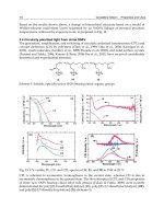
Besides the main luminescence peaks: red R, blue B, and UV an amplification of the yellow
luminescence Y at the region between 560 nm (2.2 eV) and 580 nm (2.1 eV) has been
recorded due to direct hydrogen implantation especially at RT, see Fig. 3.1. In both cases,
LNT and RT, the hydrogen implantation diminishes the red luminescence. Other authors
[Morimoto et al. 1996] have used nearly the same implantation parameters (dose and
implantation energy) as used in this study, and they reported the PL emission band at
around 2.2 eV without a detection of the 1.9 eV band. Similar results are also obtained with
He
+
implantation [Morimoto et al. 1996]. As we present in hydrogen-implanted layers, Fig.
3.1, a yellow luminescence Y at λ≈575 nm (2.1 eV) is dominating the spectra and only a weak
shoulder of the red luminescence appears. Here a high concentration of saturated bonds
≡Si−O−H or ≡Si−H ) are expected, therefore the right hand side of eq. (3.1) is fulfilled where
the NBOHC (≡Si−O●) and E´-center (≡Si●) are initially saturated by the excess hydrogen
atoms. The ≡Si−O−H bond is a good candidate to form NBOHC at room temperature in
hydrogen rich silica. The NBOHC is possibly produced by breaking the H bonds at high
annealing temperatures (T
a
>1000°C) or under electron irradiation [Kuzuu and Horikoshi
2005]. Direct hydrogen implantation or H
2
O molecule formation on the surface or in the
silica network are believed to be the main reasonable source of the Y luminescence [Fitting
et al. 2005b]; that means there are two aspects for the origin of this band.
3.2 Hydride (≡Si−H) and hydroxyl (≡Si−H−O) in SiO
2
:H
+
Hydrogen is a ubiquitous impurity in SiO
2
, therefore some authors consider it an intrinsic
defect. It is well known that hydrogen is present in all forms of silica. The wet oxide is
proposed to contain around 10
19
cm
-3
OH groups (in the form of silanol or interstitial water
molecules), while the typical OH concentration in dry oxides is only 10
16
cm
-3
.
Interstitial hydrogen does not form covalent bonds with the network, and the hydrogen
molecule does not react with the defect-free silica lattice [Blöchl 2000]. It has no states in the
band gap of silica. Thus it may be difficult to activate the hydrogen molecule with UV light
in the absence of other defects. This result indicates that hydrogen molecules need to
Crystalline Silicon – Properties and Uses
190
G
UV
B
R
SiO :H -
2
RTSiO :H -
2
RT
6 5 4 3 2.5 2 1.8 1.6
energy (eV)
UV
B
R
6 5 4 3 2.5 2 1.8 1.6
energy (eV)
CL-intensity (a.u.)
SiO :H-LN
2
TSiO :H - LN
2
T
Y
0
100
200
300
400
500
600
700
800
1h
1sec
1min
0
300
600
900
1200
1500
1800
1h
1sec
1min
200 300 400 500 600 700 800
wavelength (nm) wavelength (nm)
200 300 400 500 600 700 800
Y
G
Fig. 3.1 Initial (1sec) and saturated (5h) and dose-dependent CL spectra of H
+
implanted
SiO
2
layers recorded at room temperature (RT) and liquid nitrogen temperature (LNT).
interact with defects in silica before they can be activated. That means interstitial H
2
molecules could react at least with broken or strained silicon bonds, as
≡Si···O−Si + H
2
→ ≡Si−H + H−O−Si≡ (3.4)
or
D + H
2
→ ≡Si−H + H−O−Si≡ (3.5)
where D is an unspecified defect site. As we see, the product of the majority of the chemical
interactions proposed so far is saturated defects which can be a source (precursors) for
radiation induced defects later. In addition, hydrogen processing of the glass has been
found to greatly improve the radiation resistance because it is suspected to reduce the
number of precursors of radiation-induced defects [Brichard 2003]. It has been believed that
OH bonds make the silica system softer and better able to resist the creation of many kinds
of defects [Kuzuua and Horikoshi 2005].
G
UV
B
R
SiO :H -
2
RTSiO :H -
2
RT
6 5 4 3 2.5 2 1.8 1.6
energy (eV)
UV
B
R
6 5 4 3 2.5 2 1.8 1.6
energy (eV)
CL-intensity (a.u.)
SiO :H - LN
2
TSiO :H - LN
2
T
Y
0
100
200
300
400
500
600
700
800
200 300 400 500 600 700 800
wavelength (nm) wavelength (nm)
200 300 400 500 600 700 800
Y
G
0
500
1000
1500
2000
2500
3000
non annealed
= 700 C
= 900 C
=1100 C
T
T
T
a
a
a
o
o
o
a
non annealed
= 700 C
= 900 C
=1100 C
T
T
T
a
a
a
o
o
o
a
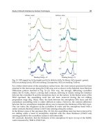
Fig. 3.2 Initial (1sec) CL spectra of H
+
implanted SiO
2
layer at different annealing
temperatures, 700≤T
a
≤1100 °C, recorded at RT and LNT.
Silicon Nanocluster in Silicon Dioxide: Cathodoluminescence,
Energy Dispersive X-Ray Analysis and Infrared Spectroscopy Studies
191
With additional hydrogen implantation we expect higher concentrations of both hydride
(≡Si−H) and hydroxyl (≡Si−O−H) in the whole network which we consider as a first
suspect for the dominant yellow luminescence in Fig. 3.1. If this hypothesis is correct, the
yellow luminescence should possibly diminish by eliminating hydrogen from the system.
Releasing hydrogen atoms even from amorphous material is previously reported by
thermal treatment [Pan and Biswas 2004]. The samples have been thermally annealed up
to relatively high temperature (T
a
) so that we can state that we were able to break the
hydrogen bonds and let an amount of hydrogen out. Fig. 3.2 shows a comparison between
the non-annealed and those thermally annealed. We found a slight change in the intensity
of the yellow luminescence at T
a
=700 °C at both RT and LNT, which means that T
a
=700 °C
is not enough yet to make a significant change in ≡Si−H and ≡Si−O−H concentration. But
by increasing the thermal annealing temperature to 900 and 1100 °C, we found a
considerable change in the CL spectra. We see diminishing of the yellow luminescence
and growing of the red luminescence R, leading us to the conclusion that T
a
>900 °C can
release hydrogen from both hydride and hydroxyl. The effective diffusion coefficient of
hydrogen and the rate of ≡Si−O−H and ≡Si−H in hydrogen rich silica glass have been
measured using Infrared spectroscopy [Lou et al. 2003]. It is found that the concentration
of both ≡Si−O−H and ≡Si−H decreases due to sample thermal treatment, see Fig. 3.3. The
decrease in hydroxyl quantity is very slow at 750 °C compared with other higher
temperatures (1000, 1250 and 1500 °C). More and faster elimination of hydroxyl is
achieved by increasing the temperature. A similar change in hydride quantity is also
shown in Fig. 3.3. Our samples have been annealed for 3600 sec (the red vertical dashed
line in Fig. 3.3) in vacuum, up to this period of time and T
a
=1100 °C we can estimate that
around 80% of hydride and hydroxyl have been eliminated from the SiO
2
:H. In Fig. 3.4
(top), we signify the dose behavior of the yellow Y and the red R luminescence. The
yellow band intensity shows higher initial level in the non annealed samples, it decreases
by increasing T
a
, but it passes a maximum at around 100 sec of electron beam irradiation.
This means that other precursors for the yellow luminescence are produced. We consider
short-term-living water molecule formation in the network to be one of these precursors.
When H
2
O molecules dissociate under the electron beam irradiation the yellow band
starts to decrease.
0 5000 10000 15000 20000 25000 30000
0.0
0.1
0.2
0.3
0.4
0.5
0.6
0.7
0.8
0.9
1.0
time (sec)
normalized residual hydroxyl
750 C
o
1500 C
o
1250 C
o
1000 C
o
750 C
o
1000 C
o
1250 C
o
1500 C
o
0 5000 10000 15000 20000 25000 30000
0.0
0.1
0.2
0.3
0.4
0.5
0.6
0.7
0.8
0.9
1.0
time (sec)
normalized residual hydride
Si HSi H
=
=
SiOHSi O H
=
=
Fig. 3.3 Normalized residual quantities of hydride (≡Si−H) and hydroxyl (≡Si−O−H) as a
function of heat treatment time in air. Open circle: 750 °C, filled circle: 1000 °C, open square:
1250 °C, filled square: 1500 °C, [Lou et al. 2003].
Crystalline Silicon – Properties and Uses
192
Contrary to the yellow luminescence, the red luminescence has much lower intensity in non-
annealed samples and rises with increasing annealing temperature T
a
until it shows the
same dose behavior as the non-implanted wet a-SiO
2
layers as articulated in the previous
section. We observe the same CL spectra and dose behavior of the red R luminescence in
SiO
2
:H as well as wet oxide SiO
2
samples at T
a
=1100 °C, see Fig. 3.4 (bottom). Finally we can
confirm the following production mode, eq. (3.6), of the non-bridging oxygen hole centers
(NBOHC, ≡Si−O●), the source of the red R luminescence in wet oxide SiO
2
, where hydrogen
and hydroxyl are present.
≡Si−O−H → ≡Si−O● + H
o
(3.6)
0
100
200
300
400
500
600
700
800
CL-intensity (a.u.)
Y: 575 nm , at RTY: 575 nm , at RT
non annealed
T
a
= 700 C
o
T
a
= 900 C
o
T
a
= 1100 C
o
0
200
400
600
800
1000
1200
Y: 565 nm , at LNTY: 565 nm , at LNT
non annealed
T
a
= 700 C
o
T
a
= 900 C
o
T
a
= 1100 C
o
1000
1500
2000
2500
3000
0
1 10 100 1000 10000
irradiation time (sec)
R: 665 nm , at LNTR: 665 nm , at LNT
non annealed
T
a
= 700 C
o
T
a
= 900 C
o
T
a
= 1100 C
o
300
400
500
600
0
1 10 100 1000 10000
irradiation time (sec)
CL-intensity (a.u.)
R: 645 nm , at RTR: 645 nm , at RT
non annealed
T
a
= 700 C
o
T
a
= 900 C
o
T
a
= 1100 C
o
Fig. 3.4 The dose-dependent of the yellow band Y (top) and the red band R (bottom) in
SiO
2
:H at different annealing temperatures recorded at RT and LNT.
3.3 H
2
O molecules and the yellow luminescence
The interaction of water molecules especially with the surfaces of amorphous silica is of
great technological interest [Legrand 1998], and thus numerous studies have been devoted
to this issue focusing especially on IR spectroscopy. It is suggested that the possible
existence of small-membered (i.e. having a small number of members) Si−O rings on SiO
2
surfaces are expected to be the reactive centers for the interaction with water and other
molecules [Mischler et al. 2005]. Additionally it is well known that water may dissociate on
SiO
2
surfaces resulting in the formation of silanol (≡Si−O−H) groups. In particular it is
frequently believed that the silanol groups are a result of the interaction of water molecules
with small-membered rings [Mischler et al. 2005], see Fig. 3.5. Besides, some experimental
results in the literature [Morimoto and Nozawa 1999] suggest that the photon irradiation of
isolated ≡Si−O−H can lead to the formation of some hydrogen bonds between the hydroxyls
and the H bonded ≡Si−O−H, which is decreased by heating to form once again isolated
≡Si−O−H and some H may be released.
Silicon Nanocluster in Silicon Dioxide: Cathodoluminescence,
Energy Dispersive X-Ray Analysis and Infrared Spectroscopy Studies
193
O
O
O
O
O
Si
Si
Si
O
O
O
Si
O
O
O
Si
O
O
H
H
O
Si
O
O
Si
Si
O
O
water
Si O rings
-
O
O
O
O
O
Si
Si
Si
O
O
O
Si
O
O
O
Si
O
H
H
O
Si
O
O
Si
Si
O
O
silanol groups
O
O
O
O
O
Si
Si
O
O
O
Si
O
O
O
Si
O
H
H
O
Si
O
O
Si
Si
O
O
H bond
O
hn
T
a
T
a
O
Si
Fig. 3.5 The speculated equilibria showing the interaction of H
2
O molecules with surface
SiO
2
rings followed by a photochemical reaction of the ≡Si−O−H to the hydrogen bond. The
dotted red line indicates the H bonding between H and O atoms, [modified after Mischler et
al. 2005, Morimoto and Nozawa 1999].
Based on IR absorption spectra described by [Rinnert and Vergant 2003], the adsorption of
water is favored by silicon dangling bonds (E´-center: ≡Si●) to form silanol groups not only
on the surface but also in the silica network. The reaction between water molecules and the
SiO
2
is supported too by the same authors, leading to the formation of two ≡Si−O−H.
With some complexities we were able to produce a thin layer of ice on the surface of pure
wet SiO
2
layer, whose CL behavior have presented in Fig. 3.6. Here we could measure the
CL spectra of ice together with the typical CL spectra of SiO
2
, see Fig. 3.6. Very intense
yellow Y luminescence has been detected, even higher than the red R luminescence of SiO
2
.
An additional sharper band in the UV range (λ≈370 nm) is also clearly seen. The width of
this band is much smaller than the conventional a-SiO
2
band widths indicating a crystalline
structured H
2
O. The whole spectral shape presented in Fig. 3.6 is loses its outlined profile in
quite short time. We see that it is no longer possible to detect a luminescence band after
some thirty seconds, especially the sharp band at 370 nm is totally disappearing.
A photoluminescence band at 3.7 eV (≈340 nm) has been reported in water-treated sol-gel
synthesized porous silica. The authors have correlated this PL emission band indirectly to
isolated silanols especially in the surface region [Yao et al. 2001], but others favored more
the interacting OH-related centers [Anedda et al. 2003b].
0
50
100
150
200
250
300
30 sec
1 sec
100 sec
200 300 400 500 600 700 800
wavelength (nm)
CL-intensity (a.u.)
6 5 4 3 2.5 2 1.8 1.6
energy (eV)
G
UV
B
R
Y
thin ice layer on SiO - LN
2
Tthin ice layer on SiO - LN
2
T
370 nm
570 nm
Fig. 3.6 CL spectra of a thin ice layer (H
2
O) on SiO
2
.
To determine whether the additional features presented in Fig. 3.6 belong to water
molecules on the surface or not, we performed the same experiment where a thicker ice
layer was produced on a metallic surface this time. To avoid any other influences coming
from the substrate material, the metallic substrate was examined first; it gave absolutely no
Crystalline Silicon – Properties and Uses
194
CL signals in our sensitive detection region. The possibility of ice bilayers on metallic
surfaces has been reported previously [Ogasawara et al. 2002]. It was found that half of the
water molecules bind directly to the surface metal atoms and the other half are displaced
toward the vacuum in the H-up configuration.
Ice layers on a metallic substrate show similar initial spectra with both 570 and 370 nm emitted
CL bands; they start with very stable intensities but the intensities fall down rapidly due to the
heat produced by the electron beam where the ice layer begins to melt then, see Fig. 3.7.
ice layer on metallic substrate - LNTice layer on metallic substrate - LNT
6 5 4 3 2.5 2 1.8 1.6
energy (eV)
UV:370 nm
CL-intensity (a.u.)
200 300 400 500 600 700 800
wavelength (nm) irradiation time (sec)
0
50
100
150
200
Y
30 min
1 sec
100 sec
UV
1 10 100 1000
0
50
100
150
200
Y: 570 nmY: 570 nm
570 nm
370 nm
Fig. 3.7 CL spectra of thin ice (H
2
O) layer on a metallic substrate (left), the dose behavior of
the individual luminescence bands (right).
Thus we state that both the fast decreasing yellow Y band at 570 nm, 2.15 eV (formerly
called green-yellow band G) as well as the long-term irradiation Y band is the same
electronic state and all attributed to water. In the first case condensed water and ice
sublimate at LNT from the surface whereas the longer irradiation Y band is due to water
molecules formed in the SiO
2
network by radiolytic processes.
3.4 Hdrogen association in luminescence defects
Extrapolating from the facts presented up to now we can formalize a model for the different
luminescence properties of the radiation induced defects in a-SiO
2
, presented in Fig. 3.8. We
assume that strained bonds ≡Si−O···Si≡ in dry oxide and the hydroxyl species (≡Si−O−H)
in wet oxide are the prevailing main precursors of the red R luminescence associated with
non-bridging oxygen hole center (NBOHC: ≡Si−O●).
During electron beam irradiation both precursors are transformed to NBOHC. We see that
the NBOHC centers produced in dry oxide increase up to a certain concentration obtained
by an equilibrium of center generation and electron beam induced dissociation to the E´-
center (≡Si●) and mobile atomic oxygen O
mob
. The production and the role of mobile oxygen
have already been stressed by [Skuja et al. 2002 and Fitting et al 2002b]. There, a model and
respective rate equations are given for the temperature and dose dependence of both the red
R and the blue B bands. The re-association of mobile oxygen to the E´-centers and re-
creation of the NBOHC will increase the role of mobile oxygen and hydrogen. Experiments
had suggested that the ≡Si−O−H is resisting bond breakage effectively at relatively short
irradiation time. Bond breakage might saturate only at sufficiently long irradiation time
[Kuzuu and Horikoshi 2005]. Different properties are shown by the wet oxide in Fig.3.8.
Silicon Nanocluster in Silicon Dioxide: Cathodoluminescence,
Energy Dispersive X-Ray Analysis and Infrared Spectroscopy Studies
195
Here the hydrogen is dissociated from the silanol group of the non-bridging oxygen bond,
eq. (3.6). But then the red luminescence of the NBOHC is destroyed by further electron beam
dissociation as in dry oxide too. The dissociated mobile hydrogen H
mob
may react with the
mobile oxygen O
mob
to form molecules H
2
, O
2
, and H
2
O on interstitial sites. These reactions
have been recently described [Bakos et al. 2004a]. There the authors underlined that water
and oxygen molecules are participating in various defect formation processes in thermally
grown SiO
2
films as well as in synthetic silica glasses. Formation energies and energy
barriers are obtained by first-principles calculations and compared for different reactions. A
part of the H atoms on the right-hand side of eq. (3.6) must form H
2
molecules through the
diffusion of H atoms in the silica network. In addition to H
2
molecules produced by this
mechanism, interstitial H
2
molecules are expected to exist in the sample. These H
2
molecules
and interstitial H
2
molecules could react with broken or strained bonds and form ≡Si−H and
≡Si−O−H pair as in eq. (3.4).
The ≡Si−H structure on the right hand side of eq. (3.4) can be a precursor of the E´-center
through the process expressed in the reverse of eq. (3.1). The amount of H
2
molecules
created by the irradiation must increase with increasing OH content. In addition to the
creation of hydrogen molecules from the ≡Si−O−H species, interstitial H
2
molecules exist
especially in the wet samples. Therefore, an excess amount of E´-centers, relative to that of
NBOHC, is induced as shown in Fig. 3.8.
Water molecules may cluster in the bigger voids of the oxide, i.e., form hydrogen-bonded
complexes with each other and the silica network's O atoms [Bakos et al. 2004a]. In such cases
two H
2
O molecules may react with each other forming once more OH bonds. Thus, the red
luminescence is stabilized at some fraction of the number of OH bonds. This model of the
hydrogen effect is consistent with our previous model of center transformation based on the
mobile oxygen generation and re-association [Fitting et al. 2002b], and extends it by the
reactions of H, OH, and H
2
O with the radicals in the silica atomic network as shown in Fig. 3.8.
This model is supported by investigations of the yellow Y luminescence, where the yellow
luminescence at the beginning of irradiation at LNT is associated with sublimating ice from the
sample surface rather more probably than due to a self-trapped exciton (STE) luminescence as
often emphasized [Trukhin 1994]. Moreover, the yellow Y luminescence after longer
irradiation (2 As/cm
2
), especially in hydrogen implanted samples, could be associated with
water molecules H
2
O too, formed in radiolytic processes as demonstrated in Figs. 3.6 and 3.7.
4. Group IV elements implanted in SiO
2
Ion implantation into glasses results in network damage and in compositional changes, it
modifies silica's physical properties such as density, refractive index, surface stress,
hardness, and chemical durability. Compositional changes can also occur due, e.g., to
radiation-enhanced diffusional losses of alkali ions, crystallization, phase separation, and H
incursion. Many authors [Hosono et al. 1990, Morimoto et al 1996, Fitting et al. 2002b,
Magruder et al. 2003] have implanted several kinds of ions in silica glass and found that ion
implantation causes an increase in refractive index by 1%-6% owing to the compaction of
surface region and to a chemical change in the structure of glass. It was deduced that this
refractive index change is caused by the formation of Si\textendash Si homobonds, but not
by the decrease in Si−O−Si bond angle which leads to compaction. In addition to the
compaction, the chemical change in structure, and the formation of colloid particles, ion
Crystalline Silicon – Properties and Uses
196
+
Si
E´ centerE´ center
Si
O
Si
strained bond
IRRADIATIONIRRADIATION
saturated bond
Si O H
+
Si
O
NBOHC
red band (R)red band (R)
"wet" oxide
"dry" oxide
Si
H
HO
2
O
2
PRECURSORS
H
mob
Si
E´ centerE´ center
H
2
O
mob
yellow band (Y)
+
e
-
Fig. 3.8 Model of the red luminescent center (NBOHC) creation from different precursors in
"wet" and "dry" oxide. The center destruction and recombination by radiolytic hydrogen and
oxygen dissociation and re-association will lead to a dynamic equilibrium.
implantation in silica glass is always accompanied by the formation of defects, such as
oxygen vacancy, E´-center, NBOHC, and peroxy radicals, resulting not only in changes to
emission bands but also to the emission of new CL bands especially in the violet V or in the
ultraviolet UV regions.
Before we start reviewing our results, it is appropriate to keep in mind that there are species
which diffuse through the glass without modifying the structure of the matrix, and these are
called non-interacting elements. There are both interstitial and substitutional non-interacting
species. Species which modify the structure of the glass matrix are called interacting species
[Minke and Jackson 2005]. Carbon (C), silicon (Si), Germanium (Ge), tin (Sn) and lead (Pb)
are the dopants whose influence on silica's natural luminescence defects will be discussed in
this section. They are examples of non-interacting substitutional species. Since these
elements have similar bonding characteristics to silicon, they can replace silicon in the
matrix of the glass, without significantly changing the network structure. Substitutional
non-interacting elements diffuse much more slowly than interstitial elements. Ion
implantation results allow deeper understanding of the relationship of the structure to
dopand incorporations, which is important for the application of ion implantation wave
guide formation in optoelectronic applications.
4.1 Silicon implantation SiO
2
:Si
+
To get started with the investigation of the implanted samples, we prefer to recognize
especially the surplus of atoms from the host material in this complex many body correlated
system. We report in this section our observation of visible-light emission at room
temperature from Si
+
implanted thermally grown SiO
2
layers on silicon substrates.
Cathodoluminescence measurements were performed on silicon implanted samples using
the same experimental parameters as used for the non implanted samples. As a result of
comparison between the CL spectra of the pure and Si
+
implanted SiO
2
, we see a significant
Silicon Nanocluster in Silicon Dioxide: Cathodoluminescence,
Energy Dispersive X-Ray Analysis and Infrared Spectroscopy Studies
197
blue B luminescence emission (460 nm ; 2.7 eV) and an intense broad luminescent band in
the yellow Y region with a peak beyond 580 nm (2.1 eV) are observed especially after
annealing at high temperature (T
a
=900 °C), see Fig. 4.1. The ultra violet UV (290 nm ; 4.3 eV)
and the red R luminescence (650 nm ; 1.9 eV) are also present but with less influence due to
silicon implantation. Two additional luminescence bands can be anticipated, one in the
green G region at 490 nm (2.5 eV) and another in the red region at around 750 nm (1.65 eV).
Higher initial intensities in the thermally annealed samples were registered but all
luminescence were saturated to the same level as of the non annealed samples. The green
(490 nm ; 2.5 eV), yellow (580 nm ; 2.1 eV) and the additional red (750 nm ; 1.65) emission
bands are associated with the presence of silicon nanoclusters in the silica matrix.
200 300 400 500 600 700 800
wavelength (nm) wavelength (nm)
200 300 400 500 600 700 800
6 5 4 3 2.5 2 1.8 1.6
energy (eV)
G
UV
B
R
6 5 4 3 2.5 2 1.8 1.6
energy (eV)
CL-intensity (a.u.)
Y
1h
1 sec
1min
pure SiO
2
d
ox
= 500 nm, RT
pure SiO
2
0
100
200
300
400
500
600
700
UV
B
R
, =900 C
T
a
o
d
ox
= 500 nm, RT
SiO :Si
2
+
,=900C
T
a
o
SiO :Si
2
+
Y
G
0
100
200
300
400
500
600
700
1 sec
1min
1h
Fig. 4.1 CL spectra of pure and Si
+
implanted SiO
2
layers at room temperature (RT). The
initial spectra (red colored) is labeled by (1 sec) and the saturated by (1 h).
The presence of silicon nanoclusters (crystalline and amorphous) is confirmed by
transmission electron microscopy (TEM) and by means of EDX measurements.Recently,
some authors presented room-temperature photoluminescence data from silica layers
implanted with Si
+
ions of 160 keV energy excited using 292 nm excitation light from a 450
W xenon lamp [Mutti et al. 1995]. They showed the existence of a visible band peaked at 1.9
eV (620 nm) together with a broad band centered at lower energy 1.7 eV (730 nm) which was
present only after annealing at 1100 °C. They ascribed the 1.9 eV band to E´ defects created
by ion implantation in the silica matrix, while they attributed the 1.7 eV band to the
presence of silicon nanocrystals.
4.2 Germanium implantation SiO
2
:Ge
+
Typical CL spectra of Ge
+
-implanted silica layers at room temperature (RT) are shown in
Fig. 4.2. The main ultraviolet (UV) and violet (V) luminescence bands at 295 nm (4.2 eV)
and 410 nm (3.1 eV) respectively, and a green band around 535 nm (2.3 eV) are seen
predominantly on non-annealed samples even at low temperature. The well-known red
band appears also in our detection range but not as dominant band as in the standard
SiO
2
spectra. Previously we have demonstrated that the spectra of Ge-doped amorphous
SiO
2
layers are a mixture of SiO
2
and tetragonal GeO
2
. Whereas the red luminescence at
1.9 eV from the NBOHC of the SiO
2
matrix is conserved, the larger amplitude of the violet
band at 3.1 eV seems to be overtaken from tetragonal GeO
2
modification indicating a
Crystalline Silicon – Properties and Uses
198
strong defect luminescence at the Ge dopant centers in the rutile-like tetragonal
coordination [Barfels 2001].
wavelength (nm)
200 300 400 500 600 700 800
G
UV
B
R
6 5 4 3 2.5 2 1.8 1.6
energy (eV)
UV
R
6 5 4 3 2.5 2 1.8 1.6
energy (eV)
CL-intensity (a.u.)
300
600
900
1200
1500
5h
30 sec
1h
1 sec
1min
0
10000
20000
30000
40000
50000
200 300 400 500 600 700 800
wavelength (nm)
0
SiO :Ge , non-annealed
2
+
d
ox
= 500 nm, RT
SiO :Ge , non-annealed
2
+
SiO :Ge , annealed
2
+
d
ox
= 500 nm, RT
SiO :Ge , annealed
2
+
=700 C
T
a
o
=900 C
T
a
o
=1100 C
T
a
o
V
V
Fig. 4.2 CL-spectra of Ge
+
-implanted (500nm) SiO
2
layers (implantation dose D=5×10
16
cm
-2
recorded at RT on the left hand side, demonstrating the huge violet band (V) at λ≈410 nm:
3.1 eV. The thermal annealing of the samples was performed at three different annealing
temperatures T
a
=700, 900, 1100 °C, as shown on the right hand side.
The CL spectra of pure undoped a-SiO
2
and Ge
+
-doped are similar to the local intrinsic point
defect centers associated with the fundamental silicon dioxide defect structure. The energy
positions and widths of the red R and the UV CL emissions are the same for both specimen
types within the limits of experimental uncertainty, unless the violet band (λ≈410 nm, 3.1
eV) is considered to be a well seen fingerprint of Ge related defects and covering the blue
band (λ≈465 nm, 2.7 eV) of pure SiO
2
. According to an earlier model [Skuja 1998], the violet
luminescence corresponds to the so-called twofold coordinated germanium luminescence
center ( =Ge●● ) which imperceptibly interacts with the host material atoms due to its poor
correlation in the silica glass network. However, this band could be also associated with
different phases of Ge, that is to Ge clusters as well nanocrystals located in the SiO
2
layer
[Fitting et al. 2002b], which can remarkably grow in size with increasing post annealing
temperature. In the absence of Ge impurities, the luminescent emission component observed
between 3.1-3.3 eV in oxygen deficient silica has been attributed to the recombination of a
hole trapped adjacent to a substitutional charge-compensated aluminum ion center
[Stevens-Kalceff 1998].
Furthermore, Fig. 4.2 (right) shows the CL spectra of the Ge
+
-implanted sample annealed at
700, 900, 1100 °C for 1 hour in dry nitrogen. The large emission band at 3.1 eV due to the
germanium implantation is observed and the intensity of this peak increases up to a factor
of 10-50 with increasing annealing temperature (T
a
), but it decreases rapidly with increasing
irradiation time. The concurrent changes in the various bands of the emission spectra due to
the Ge implantation are shown in Fig. 4.3.
With increasing annealing temperature up to T
a
=900 °C the CL intensity strongly increases.
Exceeding the annealing temperature up to 1100 °C, i.e. to the original oxidation
temperature, the CL intensity is reduced again and the green luminescence intensity at 535
nm is terminated (totally annealed), contrary to the violet (V) luminescence band which still
shows an enormous presence in the CL detection range. Also we see that NBOHC fades
Silicon Nanocluster in Silicon Dioxide: Cathodoluminescence,
Energy Dispersive X-Ray Analysis and Infrared Spectroscopy Studies
199
away with increasing annealing temperature (Fig. 4.3). That could be somehow a reason of
activation of various interstitial atoms at high temperatures, where electron spin resonance
(ESR) experiments have shown that the thermally activated diffusion of mobile interstitial
species can result in the annealing of defects involved in luminescent processes [Griscom
1990b]. As we stated, the violet luminescence is related to different states or phases of Ge,
namely to GeO
2
dissolved in the near SiO
2
surface region and to Ge nanocrystals [Rebohle et
al. 2002a] located in the SiO
2
layers, see Fig. 4.4, which may be partially oxidized at their
interface to the surrounding amorphous SiO
2
matrix. The nanoclusters size are growing
with annealing temperature from 2-4 nm at T
a
=900 °C to 5-10 nm at T
a
=1100 °C as shown in
Figs. 4.5 and 4.6.
CL-intensity (a.u.)
R : 645 nm , 1.9 eVR : 645 nm , 1.9 eV
CL-intensity (a.u.)
V : 410 nm , 3.1 eVV : 410 nm , 3.1 eV
G : 535 nm , 2.4 eVG : 535 nm , 2.4 eV
1 10 100 1000 10000
irradiation time (sec)
1 10 100 1000 10000
irradiation time (sec)
1
UV : 295 nm , 4.2 eVUV : 295 nm , 4.2 eV
0
500
1000
1500
2000
5000
10000
15000
20000
0
0
500
1000
1500
2000
0
500
1000
1500
2000
non-annealed
T
a
=700 C
o
T
a
=900 C
o
T
a
=1100 C
o
non-annealed
T
a
=700 C
o
non-annealed
T
a
=700 C
o
T
a
=1100 C
o
T
a
=900 C
o
T
a
=900 C
o
T
a
=1100 C
o
T
a
=700 C
o
non-annealed
Fig. 4.3 CL bands red (R:1.9 eV ), green (G:2.4 eV), violet (V:3.1 eV) and (UV:4.2 eV) from
Ge
+
-implanted SiO
2
layers after different annealing temperatures T
a
as a function of
irradiation time; CL measured at RT.
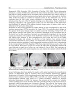
High resolution TEM micrographs shown in Fig. 4.5 reveal a spherical shape of Ge
nanocrystals in silica, in contrast to the shape of nanocrystals in other crystalline host
material. This is apparently the result of the anisotropy of the amorphous silica matrix.
Further experimental analysis of the orientation relationships between the nanocrystals and
the crystalline matrix shows that there is no fixed relationship of orientation between the
nanocrystals and the host [Xu et al. 2005]. A closer look at the highly resolved area is
obtained (marked by light colored circles) in Fig. 4.6 where higher magnification was
applied. The white circles enclose some of the nanocrystals visible under this magnification.
The crystalline structure (lattice) pattern of germanium nanoparticles is clearly
distinguishable from the amorphous host, in some areas similar even smaller crystal lattices
overlap each other. The host matrix remains in amorphous phase surviving the implantation
and thermal annealing.
The size distribution of the Ge nanocrystals was obtained through a laborious TEM effort of
a micrograph of very thin cross-sectional TEM specimen, and then followed by manually
measuring the size of the nanocrystals. The result is shown in Fig. 4.7. The dark bar
.
Crystalline Silicon – Properties and Uses
200
surface substrateinterface
R
p
SiO
2
Si
energy transfer (eV/nm)
depth (nm)
0 100 300 400 500 600 700
80
70
60
50
40
30
20
10
0
12 keV
10 keV
2 keV
3 keV
4 keV
5 keV
6 keV
8 keV
15 keV
25 keV
30 keV
E
o
=1 keV
200
Ge
100 nm100 nm
Ge implantation profile
+
SiO
2
SiO
2
Si
Ge
surface
interface
Fig. 4.4 Electron beam excitation densities in SiO
2
layers on Si substrate for different beam
energies E
o
allowing a CL depth profiling. Here we show the Ge
+
implanted SiO
2
in the
mean projected range R
p
=250 nm by an ion energy E
Ge+
=350 keV shown by the shaded
Gaussian shaped region. On the right hand side a scanning transmission electron
microscope (STEM) image of the same sample showing the actual Ge cluster profile after
thermal annealing.
20 nm20 nm 20 nm20 nm
T
a
=900 C
o
T
a
=1100 C
o
Fig. 4.5 Scanning transmission electron microscope (STEM) images of germanium implanted
SiO
2
sample annealed at: T
a
=900, 1100 °C, showing the actual size of the Ge clusters.
histogram shows the size distribution of Ge nanocrystals embedded in silica produced at
T
a
=1100 °C and the light bars are the size distribution of nanocrystals formed at T
a
=900 °C.
The Ge nanocrystals at higher temperatures are larger on average and have a wider size
distribution than those formed at lower temperatures, as it was expected. The size
distribution of the germanium particles in the silica system is near-Gaussian-shaped,
corresponding to average diameters of 3 nm and 6 nm for T
a
=900 and 1000 °C, respectively.
The cluster density is also shown in Fig. 4.7, where the cluster concentrations are
N
c
=4.6×10
17
and 2.6×10
17
cm
-3
for T
a
=900 and 1100 °C, respectively. It is expected that
thermally treating the samples is not the only reason for nanocluster formation but also
Silicon Nanocluster in Silicon Dioxide: Cathodoluminescence,
Energy Dispersive X-Ray Analysis and Infrared Spectroscopy Studies
201
5nm5 nm 5nm5 nm5nm5 nm
T
a
=900 C
o
T
a
=1100 C
o
Fig. 4.6 HR-TEM micrograph of Ge-implanted SiO
2
layers after 1 h anneal at 900 , 1100 °C.
Selective areas in the host matrix showing the growing of the crystalline Ge spots with
increasing temperature.
12345678910111213
0
5
10
15
20
25
30
35
cluster size (nm)
d
frequency (a.u.)
900 C
o
1100 C
o
900 C
o
1100 C
o
0 1020304050
0
5
10
15
20
25
distance (nm)
r
Fig. 4.7 Germanium cluster diameter and separation distance distributions: the correlated
cluster concentrations are N
c
=4.6×10
17
and 2.6×10
17
cm
-3
for T
a
=900 and 1100 °C,
respectively.
heavy electron beam irradiation, where Ge atoms diffuse faster in the more damaged area
caused by the irradiation. Large nanocrystals are thus formed, whereas in the area where Ge
atoms are less mobile, smaller nanocrystals are formed.
Based on the assessments specified in this section , we are presenting a model in Fig. 4.8 of
the annealing process forming Ge aggregates with an optimum size for a maximum
luminescence at annealing temperatures near T
a
=900 °C. For higher annealing temperatures
T
a
≥1100 °C the cluster or crystal growth has continued, thus their luminescent surface or
surroundings in their sum has been reduced, i.e. the overall luminescence efficiency
decreases. Simultaneously the specific depth of luminescent Ge clusters, however now in a
lesser amount, has shifted towards the surface, whereas at greater depths we find bigger Ge
crystallites but much less effective in luminescence than the smaller clusters.
Crystalline Silicon – Properties and Uses
202
layer depth (nm)
Ge
n (x)
CL
SiO :Ge
2
SiO :Ge
2
0 100 200 300 400 500 0 100 200 300 400 500 0 100 200 300 400 500
0 100 200 300 400 500 0 100 200 300 400 500 0 100 200 300 400 500
T
a
=900 C
o
T
a
=1100 C
o
non-annealed
Fig. 4.8 Schematic presentation of the luminescent center depth profile as a function of post
annealing temperature T
a
(above) and the supposed depth distribution of Ge nanocrystals
(below) with an optimum size for maximum luminescence (middle part).
4.3 Carbon implantation SiO
2
:C
+
Carbon implantation, like other ion implantations, produces many different chemical
reactions. It has been observed that the implanted carbon in silica can form carbon dioxide
(CO
2
) and carbon monoxide molecules (CO) [Perez-Rodriguez, et al. 2003]. It is intriguing
that the CO and CO
2
formed in the silica matrix have a very different spectroscopic
behavior from that of the gas phase molecules. These differences may reveal the unique
physical statuses of the CO and CO
2
embedded in the matrix. C
+
implantation is usually
combined with Si
+
implantations (Si rich SiO
2
layers), whereas in SiO
2
layers implanted
only with C
+
ions, it has been evidenced early on that a severe drawback consists in the
strong outdiffusion of the implanted carbon during the thermal process. This is caused by
the formation of highly mobile CO species. Accordingly, these phenomena could be
prevented by annealing under high-vacuum conditions. However, the most interesting
approach to stabilize the implanted C profile is the previous existence of a high Si
supersaturation, which enhances the interaction of both C and O atoms with the Si atoms,
and prevents the formation of C−O bonds. In this respect, we discuss the CL spectra of C
+
implanted silica.
High dose sequential implantation of C
+
ions into the SiO
2
oxides followed by high-
temperature annealing (T
a
=900 °C) probably results in the mixture of violet-blue-green-
yellow luminescence. The observed visible luminescence bands have been correlated
with the implant and annealing conditions and with the microstructure of the processed
films.
Silicon Nanocluster in Silicon Dioxide: Cathodoluminescence,
Energy Dispersive X-Ray Analysis and Infrared Spectroscopy Studies
203
UV
B
R
6 5 4 3 2.5 2 1.8 1.6
energy (eV)
B
R
6 5 4 3 2.5 2 1.8 1.6
energy (eV)
CL-intensity (a.u.)
200 300 400 500 600 700 800
wavelength (nm) wavelength (nm)
200 300 400 500 600 700 800
1h
1 sec
1min
1h
1 sec
SiO :C , RT
2
+
SiO :C , RT
2
+
SiO :C , LNT
2
+
SiO :C , LNT
2
+
G/Y
V
1min
660 nm
565 nm
460 nm
650 nm
550 nm
460 nm
295 nm
200
400
600
800
1000
0
400
800
1200
1600
2000
0
335 nm
395 nm
500 nm
UV
295 nm
335 nm
V
395 nm
G/Y
Fig. 4.9 CL-spectra of C
+
-implanted (500nm) SiO
2
layers (implantation dose D=5×10
16
cm
-2
recorded at RT and LNT. The sample was thermally annealed at T
a
=900 °C.
Fig. 4.9 demonstrate the CL spectra of C
+
implanted SiO
2
layers at room temperature (RT)
and liquid nitrogen temperature (LNT). A significant difference due to the measured
temperature change has not been registered. In general, it is more similar to the CL spectra
of Si
+
implanted silica than Ge
+
implanted silica (Figs. 4.1 and 4.2). Here we see a significant
blue B luminescence emission (460 nm ; 2.7 eV) and an intense broad luminescent band in
the green-yellow G/Y region with a peak beyond 565 nm (2.2 eV). The ultra violet UV (290
nm ; 4.3 eV) and the red R luminescence (650 nm ; 1.9 eV) are also present but with lower
intensity than in pure SiO
2
. The expectation of another red luminescence at around 750 nm
(1.65 eV) is also possible. The only difference between the CL spectra of Si
+
and C
+
implanted samples are that two additional luminescence bands in UV and V regions are
excited. One is at 335 nm (3.7 eV) and the other at around 395 nm (3.1 eV). Luminescence at
335 nm is reported in AlGaN [Riemann et al. 2002], in Lu
3
Al
5
O
12
films [Zorenko et al. 2005]
and even in crystalline SiO
2
(α-quartz) coated with LiNbO
3
[Siu et al. 1999], but never in
normal or carbon implanted silica. The violet V luminescence comes into view at a lower
wavelength, 394 nm, where this luminescence band was detected in the wavelength range
400-410 nm in other implanted silica layers, as we have already demonstrated in Ge
+
implanted SiO
2
. We found this band in all ion implanted samples which means that the
violet luminescence is not only created due to a specific ion kind implanted in silicas but
part of it arises from the network damage caused by the ion beam bombardment. Here the
intensity of the V band is lower compared to CL spectra of other ion implanted samples
presented in this study. We propose that some carbon atoms have been diffused out of the
network due to samples thermal treatments.
The intense room-temperature luminescent bands from the blue up to the yellow spectral
region as a result of C
+
ion-implantation processes into SiO
2
layers have been reported by
several authors [Zhao et al. 1998, Yu et al. 1998, Rebohle et al. 2001b]. There is a general
consensus in assigning these bands to the formation of C-related nanoparticles. The green-
yellow luminescence band (2.0-2.2 eV) was also observed in the C
+
implanted SiO
2
layers. In
this case, the intensity of the luminescent band was well correlated with the contribution of
carbon-related nanoclusters. A luminescence band at higher energies, in the range of 2.7 eV,
has also been reported from carbon graphite-like nanoparticles embedded in SiO
2
layers
synthesized either by ion implantation [Yu et al. 1998, Gonzalez-Verona et al. 2002] or by
Crystalline Silicon – Properties and Uses
204
sputtering deposition of C-rich oxides [Zhang et al. 1996] followed by thermal annealing.
The blue luminescent band is also characteristic of SiC-related crystalline nanostructures, as
porous SiC [Ma et al. 2000]. Furthermore, some authors have analyzed the PL emission from
C
+
implanted SiO
2
and they attributed the luminescent bands in the blue region to the
formation of amorphous clusters of Si
y
C
1-y
O
x
complexes [Rebohle et al.2001b]. The
microstructure of carbon implanted silica was investigated by Auger electron spectroscopy
(AES) and transmission electron microscopy (TEM). Amorphous nanostructures with a size
between 2 and 3.5 nm were found in a depth region between 80 and 150 nm below the oxide
surface. Strong photoluminescence (PL) around 2.1 and 2.7 eV has also been observed after
excitation at 4.77 eV as an indication of nanoclusters [Rebohle et al. 2001b].
4.4 Tin implantation SiO
2
:Sn
+
The implantation of Sn ions into SiO
2
layers has been studied in connection with the
formation of defects and nanostructures exhibiting intense visible and ultraviolet
Cathodoluminescence (CL). The spectra of Sn
+
implanted SiO
2
is dominated by a strong
violet V emission band with the intensity maximum at about 400 nm and a faint shoulder of
the blue luminescence at its usual position in SiO
2
spectra (around 460 nm), see Fig. 4.10. It
seems that another UV band is overlapped with the UV band detected previously at 290 nm,
or it could be that the 290 nm luminescence band has shifted to a higher wavelength
position at around 320 nm. An emission band at 320 nm is attributed to bulk tin dioxide
[Lopes et al. 2005a, Calestani et al. 2005]. Tin dioxide (SnO
2
) is an n-type semiconductor with
a wide band gap (E
g
=3.6 eV at 300 K) and is particularly important for many electronic
applications. At low temperature (10 K) the intensity maximum of the UV band experiences
a blue shift of about 10 nm.
G
UV
B
R
6 5 4 3 2.5 2 1.8 1.6
energy (eV)
UV
B
R
6 5 4 3 2.5 2 1.8 1.6
energy (eV)
CL-intensity (a.u.)
200 300 400 500 600 700 800
wavelength (nm) wavelength (nm)
200 300 400 500 600 700 800
Y
1h
1 sec
1min
1h
1 sec
SiO :Sn , RT
2
+
SiO :Sn , RT
2
+
SiO :Sn , LNT
2
+
SiO :Sn , LNT
2
+
G/Y
0
2000
4000
6000
8000
10000
12000
14000
0
2000
4000
6000
8000
10000
12000
14000
V
IR
1min
IR
V
310 nm
760 nm
655 nm
545 nm
460 nm
760 nm
655 nm
530 nm
460 nm
400 nm
320 nm
400 nm
Fig. 4.10 CL-spectra of Sn
+
-implanted (500nm) SiO
2
layers (implantation dose D=5×10
16
cm
-2
)
recorded at RT and LNT. The sample was thermally annealed at T
a
=900 °C.
A broad band G peaked at about 530 nm is revealed in room temperature (RT) CL spectra;
this band was assigned to Sn nanobelts (or Sn rings) with a lateral dimension 50 nm to 1000
nm. Smaller nanobelts were assigned with longer wavelength position in the CL spectra. At
LNT the G/Y shifts 15 nm forward to the red region. In addition, the formation of a rather
dense array of Sn-rich nanoparticles presenting a narrow size dispersion and located within
the oxide but very close to the SiO
2
/Si interface has been observed [Lopes et al. 2005a]. More
Silicon Nanocluster in Silicon Dioxide: Cathodoluminescence,
Energy Dispersive X-Ray Analysis and Infrared Spectroscopy Studies
205
recently, it has been shown that the annealing atmosphere also influences the microstructure
development of Sn
+
implanted silica layers, with significant effects in blue-violet PL
response [Lopes et al. 2005a]. Sn
+
implanted samples were thermally annealed at T
a
=900 °C.
The CL bands in the V, B and G regions were associated with oxygen deficiency centers
ODC created during the implantation and annealing processes [Rebohle et al. 2000], and
probably assisted by the development of the nanoparticles system.
Data from literature [Hu et al. 2002, Hu et al. 2003] report on the evidence of broad PL
optical bands from SnO
2
nanobelts in visible wavelength range from 400 nm to 600 nm. The
nature of the transition is tentatively ascribed to nanocrystals inside the nanobelts or to Sn or
O vacancies occurring during the growth which can induce trapped states in the band gap
[Wu et al. 1997]. Other authors [Gu et al. 2003] present absorption and PL luminescence
spectroscopy on SnO
2
nanoparticles showing an absorption edge at 300 nm. The same
authors show two distinct PL emissions at 400 and 430 nm which are tentatively attributed
to Sn interstitials or dangling bonds and to oxygen vacancies respectively.
The indication of the presence of doping-related oxygen deficient centers (ODC's) was
obtained from the 5 eV absorption band. This band is supposed to arise from twofold
coordinated silicon (=Si) cation sites in pure silica, and =Ge or =Sn sites in Ge
+
doped and
Sn
+
implanted silica [Skuja 1992a, Anedda et al. 2001], as evidenced by polarized
photoluminescence and lifetime data of the emission excited in this band [Skuja 1992a].
In particular, we showed that Sn
+
doping can give rise to strong and thermally stable
luminescence bands. However, it is not clear whether the microscopic mechanisms involved
are those proposed to be responsible for the photosensitivity of Sn
+
doped silica
photoconversion of optically active defects induced by doping and structural compaction of
the doped host network.
UV
R
6 5 4 3 2.5 2 1.8 1.6
energy (eV)
B
R
6 5 4 3 2.5 2 1.8 1.6
energy (eV)
CL-intensity (a.u.)
200 300 400 500 600 700 800
wavelength (nm) wavelength (nm)
200 300 400 500 600 700 800
Y
1h
1 sec
1min
1h
1 sec
SiO :Pb , RT
2
+
SiO :Pb , RT
2
+
SiO :Pb , LNT
2
+
SiO :Pb , LNT
2
+
G/Y
1min
V
655 nm
545 nm
460 nm
655 nm
290 nm
400 nm
0
200
400
600
800
1000
1200
0
400
800
1200
1600
2000
2400
B
455 nm
370 nm
425 nm
G
500 nm
425 nm
370 nm
UV
290 nm
Fig. 4.11 CL-spectra of Pb
+
-implanted (500 nm) SiO
2
layers (implantation dose D=5×10
16
cm
-2
)
recorded at RT and LNT. The sample was thermally annealed at T
a
=900 °C.
The red R luminescence (655 nm) is partially eliminated due to Sn
+
implantation. A probable
IR CL band can be seen in Fig. 4.10. No evidence of CL or PL emission at 760 nm is,
however, reported.
4.5 Lead implantation SiO
2
:Pb
+
The CL spectrum of the Pb
+
implanted sample is shown in Fig. 4.11. Both Sn and Pb are
classified as metallic substances in contrast to the other dopands presented in this section.
Crystalline Silicon – Properties and Uses
206
Pb
+
implantation creates defect centers providing more intense luminescence in the violet-
blue region. Here, two UV bands are detected; one is the UV of the SiO
2
matrix at 290 nm
with very low intensity and another, for sure due to Pb implantation at 370 nm. Contrary to
the violet band detected in Ge and Sn implanted silicas, the violet band in Fig. 4.11 is shifted
towards longer wavelengths (425 nm) and showing lower intensity than the blue
luminescence at 455 nm. We were anticipating the existence of a luminescence band at
exactly at 500 nm and even in pure SiO
2
. Pb
+
implantation enhanced this band significantly
at RT. The blue and the green bands suffered red shifts when the measurement's
temperature was changed to LNT.
All bands labeled in Fig. 4.11 were going through destructive modes where their intensities
dropped considerably in the first seconds of irradiation and they never recovered again as it
is often happens in pure SiO
2
CL spectra. The bands in the shorter wavelength than the red
are often ascribed to nucleation of the dopand atoms in silica, therefore we expect different
forms of Pb aggregates which destroyed under the electron beam irradiation, can be the
main precursor of these bands.
The famous red band (655 nm) has lost fractions of its intensity because of Pb
+
implantation
but it goes via destructive and creation modes simultaneously, where the NBOHC is
saturated by the dopands and followed by liberation from the dangling oxygen bonds under
heavy electron bombardment.
5. Group VI elements implanted in SiO
2
The visible cathodoluminescence from Si and its substitutional atoms at room temperature
and liquid nitrogen temperatures have been presented in the previous section. In this
section we will report the luminescence emission characterizing oxygen ion-implantation in
a-SiO
2
layers under electron beam excitation. Moreover some other elements (sulfur and
selenium) from group IV which are supposed to replace some of the oxygen atoms in the
silica matrix are important for better understanding of oxygen related radiation processes
and the structure and electronic state of respective defects while oxygen diffusion and
chemistry in SiO
2
are most important for silicon-based microelectronics.
5.1 Oxygen implantation SiO
2
:O
+
The typical CL spectra of wet SiO
2
is dominated mainly by bands: red R (650 nm, 1.9 eV),
blue B (460 nm, 2.7 eV), and UV (290 nm, 4.3 eV) besides we recognize a yellow band Y (570
nm, 2.2 eV) at LNT decaying very rapidly at the beginning of the electron beam irradiation
and CL excitation, but appearing and increasing at RT after a longer time of irradiation. We
could relate some of these bands to special luminescence defect centers. Defects rolled or
influenced by addition of oxygen are shown in Fig. 5.1 where the CL spectra of an oxygen
implanted SiO
2
layer are presented. Direct comparison between Fig. 5.1 and the CL on non-
implanted (pure) SiO
2
shows that the changes are in the red luminescence region and no
extra modification in the other regions of the spectra. This serves to confirm the origin and
the structure of the NBOHC where more strained silicon-oxygen bonds can transfer to
≡Si−O● and more interstitial oxygen can be produced depending on the implantation doses.
The red luminescence is not only associated with the NBOHC but also associated with
interstitial oxygen [Skuja et al. 1994a].
Silicon Nanocluster in Silicon Dioxide: Cathodoluminescence,
Energy Dispersive X-Ray Analysis and Infrared Spectroscopy Studies
207
UV
B
R
1h
1 sec
1min
SiO :O , =900 C
2
+
T
a
o
d
ox
= 500 nm, RT
SiO :O , =900 C
2
+
T
a
o
Y
G
0
100
200
300
400
500
600
700
800
wavelength (nm)
200 300 400 500 600 700 800
6 5 4 3 2.5 2 1.8 1.6
energy (eV)
200 300 400 500 600 700 800
wavelength (nm)
G
UV
B
R
6 5 4 3 2.5 2 1.8 1.6
energy (eV)
CL-intensity (a.u.)
Y
1h
1 sec
1min
pure SiO
2
d
ox
= 500 nm, RT
pure SiO
2
0
100
200
300
400
500
600
700
800
Fig. 5.1 CL spectra of non-annealed and annealed (T
a
=900 °C) O
+
implanted SiO
2
layers at
room temperature (RT). The initial spectra are labeled by (1 sec) and the saturated by (1 h).
5.2 Selenium implantation SiO
2
:Se
+
Se
+
was isoelectrically implanted with regard to oxygen. Fig. 5.2 shows the CL spectra
obtained from the SiO
2
layers implanted by Se
+
and annealed at 900 °C. Once again no
change is found in the UV luminescence; it is appearing at the same position with low
intensity, also the violet luminescence due to Se implantation this time at 410 nm.
The blue luminescence is also located clearly at 460 nm. The red and yellow
luminescences are enhanced by Se
+
implantation, and both bands seem to be from the
same origin as in pure SiO
2
where both have the same tendency during electron beam
irradiation at RT and LNT.
UV
B
R
1h
1 sec
1min
SiO :O , =900 C
2
+
T
a
o
d
ox
= 500 nm, RT
SiO :O , =900 C
2
+
T
a
o
Y
G
0
100
200
300
400
500
600
700
800
wavelength (nm)
200 300 400 500 600 700 800
6 5 4 3 2.5 2 1.8 1.6
energy (eV)
200 300 400 500 600 700 800
wavelength (nm)
G
UV
B
R
6 5 4 3 2.5 2 1.8 1.6
energy (eV)
CL-intensity (a.u.)
Y
1h
1 sec
1min
pure SiO
2
d
ox
= 500 nm, RT
pure SiO
2
0
100
200
300
400
500
600
700
800
Fig. 5.2 CL spectra of non-annealed and annealed (T
a
=900 °C) Se
+
implanted SiO
2
layers at
room temperature (RT) and liquid nitrogen temperature (LNT). The initial spectra are
labeled by (1 sec) and the saturated by (1 h).
5.3 Sulfur implantation SiO
2
:S
+
Defect centers in sulfur-implanted silica layers differ considerably from those observed in
other implanted samples. Fig. 5.3 shows the cathodoluminescence spectra of S
+
doped SiO
2
at room temperature (RT) and liquid nitrogen (LNT) as well as their time dependence.
Crystalline Silicon – Properties and Uses
208
Obviously, the high violet intensity V at ≈405 nm is assigned to sulfur S
+
implantation.
Moreover, a sharp and intensive multi-step emission in the green-yellow-red-nearIR (500-
820 nm) region is observed for these layers. The exact band positions in wavelengths and
energies are given in Table 5.1.
The UV band (290 nm) has been observed at the same position in both samples as well as in
pure SiO
2
. Moreover, after longer irradiation of about 1 min, i.e. an electron beam dose of 0.3
As/cm
2
, the multiplet structure disappears and the characteristic red band R (660 nm) of
the NBOHC in SiO
2
becomes visible besides remaining components at the blue band B (460
nm) position and in the yellow region at 560 nm and 590 nm. On the other hand, the
sulfur-associated violet band V (405 nm) still remains visible.
Analyzing the multiplet (MP) band structure according to the data listed in Table 5.1, we
find that the energy differences between the sub-bands start from 0.14 eV in the green
region and then decreases to 0.12 eV in the red region up to 0.11 eV in the near IR. Thus the
mean step width amounts to about 120 meV. This energy difference may correspond to a
series of almost equidistant vibration levels of non-saturated sulfur radicals ≡Si−S● or
≡Si−O−S● formed during implantation and thermal annealing analogously to the red R
band center of the non-bridging oxygen (NBOHC) ≡Si−O● in pure SiO
2
.
UV
B
R
6 5 4 3 2.5 2 1.8 1.6
energy (eV)
wavelength (nm)
200 300 400 500 600 700 800
2 sec
SiO :S , =900 C
2
+
T
a
o
d
ox
= 500 nm, LNT
SiO :S , =900 C
2
+
T
a
o
Y
0
500
1000
1500
2000
2500
3000
4 sec
8 sec
15 sec
30 sec
1 sec
1 min
1h
G
UV
B
R
6 5 4 3 2.5 2 1.8 1.6
energy (eV)
CL-intensity (a.u.)
200 300 400 500 600 700 800
wavelength (nm)
Y
SiO :S , =900 C
2
+
T
a
o
d
ox
= 500 nm, RT
SiO :S , =900 C
2
+
T
a
o
0
200
400
600
800
1000
1200
1400
1600
2 sec
4 sec
8 sec
15 sec
30 sec
1 sec
1 min
1h
650 nm
580 nm
460 nm
500 nm
530 nm
560 nm
590 nm
630 nm
670 nm
715 nm
765 nm
820 nm
G
665 nm
500 nm
530 nm
560 nm
590 nm
630 nm
670 nm
715 nm
765 nm
820 nm
460 nm
V
V
410 nm
290 nm 290 nm
410 nm
Fig. 5.3 CL spectra of non-annealed and annealed (T
a
=900 °C) S
+
implanted SiO
2
layers at
room temperature (RT) and liquid nitrogen temperature (LNT). The initial spectra are
labeled by (1 sec) and the saturated by (1 h).
Even the MP step widths decrease with lower photon energy, beginning with ∆E=140 meV
at hν=2.48 eV and dropping to ∆E=110 meV at hν=1.51 eV, indicating a widened (sub-
quadratic) potential curve of the luminescence ground states with compressed higher
vibration levels imagined in terms of the adiabatic configuration coordinate model.
5.4 Investigation of the multimodal luminescence
Before attributing this effect to sulfur implantation, we should prove whether the structured
spectrum is indeed true or arises from some experimental artifacts. We considered the
second argument in our first analysis, where contaminated layers especially at low
temperature measurements, interference (Fabry-Perot type) in thin films, and monocrystals
as quantum dots could also cause such effects temporarily. The measurements of the CL
spectra of the S
+
implanted sample have been repeated many times and under different
Silicon Nanocluster in Silicon Dioxide: Cathodoluminescence,
Energy Dispersive X-Ray Analysis and Infrared Spectroscopy Studies
209
experimental conditions; the results were always the same. Samples annealed at higher
temperatures still showed resolved multimodal bands, see Fig. 5.4, but the structured area
was less sharp, indicating a destruction of the centers causing this effect. Then any
experimental artifacts are definitely excluded.
Cluster formation is always expected especially when the samples are annealed at
temperatures exceeding 900 °C. We found no traces of sulfur clusters in our samples. Fig. 5.5
shows a STEM micrograph of the S
+
implanted silica layer in the same magnification as used
to detect Ge cluster (Fig. 5.4). S
+
implanted silica is rarely reported in the literature. Some
authors reported their PL results of S
+
doped in 1 mm thick optical fiber disks; the sulfur
content was 0.05 wt% which corresponds to 2×10
19
atoms/cm
3
. They attributed a similar
structured luminescence spectra but at a lower energy region (300-500 nm) to S
2
and S
+
2
interstitial molecules [Zavorotny et al. 2001, Gerasimova et al. 2002]. But afterwards they
concluded that the irregular intensity distribution of vibrational components of the PL
excitation band indicates that the color centers responsible for this band belong not to a
diatomic molecule with one vibrational frequency but to a polyatomic molecule whose
vibrational spectrum is formed by a combination of three vibrational frequencies.
SiO SiO :S
2 2
SiO SiO :S
2 2
ln/nm /eVh lnD/nm /eV /meVhE
290
405
500
530
560
590
630
670
715
765
820
4.30
3.10
2.48
2.34
2.21
2.10
1.97
1.85
1.73
1.62
1.51
140
130
110
130
120
120
110
110
UV
V
Y
R
IR
MP
290
460
570
660
4.3
2.7
2.2
1.9
UV
B
Y
R
Table 5.1 Luminescence bands and multiplet states (MP) in SiO
2
and sulfur implanted SiO
2
:S.
It is for this reason that they later attempted the multimodal structured spectra with the SO
2
molecule [Gerasimova 2003]. Whether this hypothesis is correct or not, we see a direct
connection between the multimodal structured luminescence and oxygen atoms where
sulfur atoms are supposed to substitute oxygen in the matrix and then more oxygen in
interstitial sites is expected because over-stoichiometric SiO
x
with x>2 does not exist.
V
G
UV
B
R
6 5 4 3 2.5 2 1.8 1.6
energy (eV)
CL-intensity (a.u.)
200 300 400 500 600 700 800
wavelength (nm)
Y
1h
1 sec
1min
SiO :S , =1100 C
2
+
T
a
o
d
ox
= 500 nm, RT
SiO :S , =1100 C
2
+
T
a
o
0
500
1000
1500
2000
2500
3000
10 sec
30 sec
Fig. 5.4 Room temperature (RT) CL spectra of annealed S
+
implanted SiO
2
at higher
temperature (T
a
=1100 °C).
Crystalline Silicon – Properties and Uses
210
SiO
2
SiO
2
Si
100 nm100 nm
Fig. 5.5 STEM micrograph of the S
+
implanted silica layer annealed at 900 °C showing no
evidence of sulfur clusters.
In order to avoid water formation and binding of oxygen we have chosen dry oxidized SiO
2
layers to run our test. Oxygen atoms were implanted in a thinner (d
ox
=100 nm) dry SiO
2
layer with lower energy (20 keV) and lower doses (3×10
16
cm
-2
). Thus the overall CL
intensity is about one order of magnitude lower than in 500 nm thick wet oxidized layers,
Fig. 5.6. Surprisingly we found the same multiple regular-shaped structure from the green G
over the yellow Y and red R regions into near infrared IR in the same peak positions, when
the sample was annealed at 1000 °C. And no trace of the violet luminescence was to be seen,
see Fig. 5.6. Such structural spectra are never recorded even by using different compositions
of non-implanted SiO
2
layers.
This leads us to the conclusion that not sulfur but oxygen should be the source of these
multimodal spectra. As already declared, oxygen is responsible for the red R luminescence
in SiO
2
.
Looking to the literature, we found excitation [Rolfe 1979] and emission spectra [Ewig and
Tellinghuisen 1991] of the negatively charged oxygen molecule O
¯
2
on interstitial sites in
alkali halide crystals. The ground electronic state and several low-lying excited states of the
superoxide ion O
¯
2
have been studied by multi-configuration self-consistent fields (MCSCF),
see Fig. 5.7. For comparison, the ground state of the neutral O
2
molecule was also
considered. Parallel computations were carried out for the species in vacuo and in a
simulated KCl crystal lattice (in lattio). Computed spectroscopic parameters are in good
agreement with experiments for X and A states of O
¯
2
in vacuo. In Fig. 5.7 there is also
substantial agreement between the computed energy curves for both the ground X and the
excited A states in a point-charge lattice and those measured in alkali halide lattices.
Further, the spectroscopic parameters of the electron scattering resonance states in vacuo
agree well with those of the analogous lattice-stabilized excited electronic states in the solid.
There is a typical absorption from the ground state X to the excited state A of about hν=5.1
eV corresponding to the red R luminescence excitation associated with the NBOHC [Skuja
1994a]. Moreover, the related luminescent transition from A→X shows the red R
luminescence at about hν=2 eV. Looking to vibronic levels within the potential configuration
curves, we see levels of about 120 meV step-widened towards higher energies, i.e towards
the green G region, Fig. 5.7. Thus we should prefer the explanation of the multimodal
spectra by means of electronic-vibronic spectra transitions as given by the common
configuration coordinate model of luminescence. All transitions appear in good agreement
with the multimodal CL spectra of SiO
2
:O and SiO
2
:S layers shown here. Therefore we favor
Silicon Nanocluster in Silicon Dioxide: Cathodoluminescence,
Energy Dispersive X-Ray Analysis and Infrared Spectroscopy Studies
211
the interstitial O
¯
2
model for the multimodal CL structure and may reject the concept of a
photonic crystal structure as proposed in [Bailey et al. 2005] as well as effects of quantum
confinement as reported recently for GaAs quantum dots in [Rodt et al. 2005]. Of course, in
the latter case of GaAs or other nanostructure materials even other molecule formations
should be taken into account as possibly responsible for different but similarly shaped
multimodal structures of luminescence spectra.
at room temperature ( RT)at room temperature ( RT) at liquid nitrogen temperature ( LNT)at liquid nitrogen temperature ( LNT)
0
10
20
30
40
6 5 4 3 2.5 2 1.8 1.6
energy (eV)
CL-intensity (a.u.)
6 5 4 3 2.5 2 1.8 1.6
energy (eV)
0
10
20
30
40
CL-intensity (a.u.)
10
20
30
40
CL-intensity (a.u.)
10
20
30
40
wavelength (nm)
CL-intensity (a.u.)
O implanted SiO , =100 nm
+
2
d
ox
initial spectra (1 sec)
saturated spectra (100 sec)
T
a
= 800 C
o
O implanted SiO , =100 nm
+
2
d
ox
T
a
= 800 C
o
O implanted SiO , =100 nm
+
2
d
ox
initial spectra (1 sec)
saturated spectra (100 sec)
T
a
= 1000 C
o
O implanted SiO , =100 nm
+
2
d
ox
T
a
= 1000 C
o
O implanted SiO , =100 nm
+
2
d
ox
initial spectra (1 sec)
saturated spectra (100 sec)
T
a
= 1300 C
o
O implanted SiO , =100 nm
+
2
d
ox
T
a
= 1300 C
o
50
100
150
200
0
50
100
150
200
50
100
150
200
50
100
150
200
O implanted SiO , =100 nm
+
2
d
ox
initial spectra (1 sec)
saturated spectra (100 sec)
T
a
= 800 C
o
O implanted SiO , =100 nm
+
2
d
ox
T
a
= 800 C
o
O implanted SiO , =100 nm
+
2
d
ox
initial spectra (1 sec)
saturated spectra (100 sec)
T
a
= 1000 C
o
O implanted SiO , =100 nm
+
2
d
ox
T
a
= 1000 C
o
O implanted SiO , =100 nm
+
2
d
ox
initial spectra (1 sec)
saturated spectra (100 sec)
T
a
= 1100 C
o
O implanted SiO , =100 nm
+
2
d
ox
T
a
= 1100 C
o
O implanted SiO , =100 nm
+
2
d
ox
initial spectra (1 sec)
saturated spectra (100 sec)
T
a
= 1300 C
o
O implanted SiO , =100 nm
+
2
d
ox
T
a
= 1300 C
o
0
0
wavelength (nm)
200 300 400 500 600 700 800
0
820 nm
R
B
Y
UV
R
B
Y
UV
R
B
Y
UV
765 nm
715 nm
665 nm
630 nm
590 nm
560 nm
530 nm
500 nm
460 nm
425 nm
295 nm
R
B
Y
UV
760 nm
710 nm
650 nm
590 nm
565 nm
520 nm
460 nm
425 nm
B
Y
295 nm
R
R
B
Y
UV
0
O implanted SiO , =100 nm
+
2
d
ox
initial spectra (1 sec)
saturated spectra (100 sec)
T
a
= 1100 C
o
O implanted SiO , =100 nm
+
2
d
ox
T
a
= 1100 C
o
0
200 300 400 500 600 700 800
R
B
Y
UV
R
B
Y
UV
Fig. 5.6 CL spectra of non-annealed and annealed (T
a
=700, 900, 1000, 1300 °C) O
+
implanted
SiO
2
layers at room temperature (RT) and liquid nitrogen temperature (LNT). The initial
spectra are labeled by (1 sec) and the saturated by (1 h).
Crystalline Silicon – Properties and Uses
212
1 1.5
2
2.5
0
1
2
3
4
5
6
internuclear distance ( )
r
D
X
A
relative energy x10 (cm )
4-1
O
2
O
2
-
.
5.1 eV
.
5.1 eV
.
2eV
.
2 eV
Fig. 5.7 Comparison of MCSCF in lattio (cycles) and in vacuo (triangles) energies with
experimental Morse curves derived from analysis of absorption, excitation and
luminescence spectra of O
¯
2
in NaCl; vibronic levels are indicated by bars [Ewig and
Tellinghuisen 1991]
6. Conclusions
The investigation of the present work are extended to various electronical and optical
modifications of silica SiO
2
layers as they are applied in microelectronics, optoelectronics, as
well as in forthcoming photonics. Electron irradiation of a-SiO
2
layers induces chemical
defect reactions dependent on the sample oxidation procedure, thermal post-annealing and
CL excitation temperature. The red luminescence R (650 nm ; 1.9 eV) is associated with the
non-bridging oxygen hole center (NBOHC: ≡Si−O●) whereas the blue luminescence B (460
nm ; 2.7 eV) and the ultraviolet band UV (4.2 eV ; 295 nm) are attributed to Si-related oxygen
deficient centers (Si-ODC). CL spectra of hydrogen-free (dry-oxidized) and hydrogen-rich
(wet-oxidized) samples have shown significant differences especially in the red region.
Hydrogen and hydroxyl groups during wet oxidization increase the intensity of the red
luminescence center, where exposure of SiO
2
during the oxidation to water vapor results in
the appearance of various OH species (Si−O−H, hydrogen bonded OH, H
2
O and the Si−H
bond). Thus the dose-dependence of the red R luminescence in wet and dry oxides differs
significantly, decreasing in wet oxide from a high initial level down to saturation and
increasing in dry oxide from almost zero to saturation. The initial decrease in the red
luminescent NBOHC concentration is indicating a recombination of NBOHC with different
types of hydrogenous species. In dry SiO
2
the strained bonds (≡Si−O···Si≡) and their
electron beam-induced rupture are the precursors for the NBOHC. The mean lifetime of the
red luminescence in wet oxide τ=(4.7±0.2)μs is almost the same as in dry oxide τ=(5.3±0.2)μs.
Additional hydrogen ion implantation into SiO
2
diminishes the intensity of the red
luminescence R because of hydrogen saturation of NBOHC, but magnifies the yellow
luminescence Y to very high intensity, even higher than the intensity of the red
luminescence. In hydrogen implanted SiO
2
the yellow Y luminescence appears after
irradiation doses of about 2 As/cm
2
and we may propose that this band is due to water
molecules in the SiO
2
network formed by mobile radiolytic hydrogen and oxygen. A
comparison with the CL of water (ice) layers supports this hypothesis.
Understoichiometric SiO
x
layers with x≤2 of oxygen deficit or silicon surplus are prepared
by means of thermal evaporation of silicon monoxide SiO
1
in different ambient oxygen
Silicon Nanocluster in Silicon Dioxide: Cathodoluminescence,
Energy Dispersive X-Ray Analysis and Infrared Spectroscopy Studies
213
atmospheres. The stoichiometric degree varies between 1≤x≤2 and was determined by FTIR
calibration measurements by means of the respective shift of the Si−O−Si stretching mode.
CL spectra of SiO
x
begin to show first typical silica luminescence bands at a stoichiometric
threshold of about x>1.4. Thermal annealing of these layers and electron bombardment lead
to a partial phase separation of SiO
x
into atomic Si fragments and clusters in a nearly
stoichiometric SiO
2
matrix. This process is correlated with the different luminescent centers
in amorphous SiO
2
. Especially the yellow luminescence 2.1 eV seems to be associated with
silicon hexamer rings in under-stoichiometric SiO
x
. Probably they represent the first step of
Si nanocrystal formation. Further on, Si clusters can grow to a size of several nanometers.
The size distribution, shown by TEM micrographs, exhibits a most probable diameter size of
4 nm and a maximum diameter up to 10 nm. Our results provide evidence that at least two
distinct defects are responsible for the yellow luminescence Y at 2.1 eV in silica. The first in
wet and H-implanted SiO
2
is due to high H
2
O molecule content which can be removed by
thermal annealing until it behaves like normal wet SiO
2
. The second defect for the yellow
luminescence in dry SiO
2
(where almost no H or H
2
O exist) could be due to oxygen deficient
centers in the form of silicon fragments or small rings in the SiO
2
network.
To investigate whether the different luminescent centers are related to oxygen or to silicon,
we have compared non-stoichiometric SiO
2
layers produced by direct oxygen or silicon ion
implantation. Thermally oxidized SiO
2
layers of 100 and 500 nm thickness have been
implanted with different kinds of ions with a dose 3×10
16
and 5×10
16
ions/cm
2
, respectively,
leading to an atomic dopant fraction of about 4 at.% in the middle, i.e. the half depth of the
SiO
2
layers. Oxygen implantation as well as, on the other hand, direct silicon implantation
led to an oxygen surplus as well as an oxygen deficit, respectively. As the main
experimental results we could state: Oxygen surplus increases the red band R in SiO
2
but
does not affect the blue band B. Silicon surplus increases the blue luminescence B, but
reduces the red band R. So it is verified that the red luminescence R is an oxygen related
center stated as NBOHC and the blue luminescence B is a silicon related oxygen deficient
center Si-ODC.
In Ge
+
-implanted SiO
2
a huge violet band V (3.1 eV ; 410 nm) appears and is associated with
the Ge-related oxygen deficient center Ge-ODC. It dominates the luminescence spectra,
covering the original blue band B (Si-ODC) of the SiO
2
matrix. Further on, the V band shows
a large increase after thermal annealing. Thus thermal annealing around temperatures of
T
a
=900 °C increases the violet luminescence of the Ge-ODC by more than two orders of
magnitude. Thus the Si-ODC's as well as the Ge-ODC's are formed by Si and Ge molecules
clustering to certain low-dimension fragments: dimers, trimers and higher aggregates. With
further annealing at higher temperatures, Si and Ge nanocrystals are formed embedded in
the amorphous SiO
2
matrix, and the blue B and the violet V luminescence begin to decrease
again. The nanocluster size grows with annealing temperature from 2-4 nm at T
a
=900 °C to
5-10 nm at T
a
=1100 °C.
Further on, heavy electron beam bombardment of SiO
2
with doses of 2.7 As/cm
2
and
associated oxygen dissociation may also create Si nanoclusters in a size range of 2-10 nm
with a most probable diameter of 4 nm. These Si nanoclusters with their quantum
confinement are a source of luminescence in the near IR at 1.6 eV and probably at 1.3 eV too.
Further ion implantations of group IV elements: C
+
, Sn
+
, Pb
+
which are thought to substitute
Si in the silica matrix, show new bands and a general increase of the luminescence in the
blue region. On the other hand, implantations of oxygen substitute elements of group VI