Photodiodes Communications Bio Sensings Measurements and High Energy Part 14 docx
Bạn đang xem bản rút gọn của tài liệu. Xem và tải ngay bản đầy đủ của tài liệu tại đây (2.26 MB, 20 trang )
Quantitative Measurements of X-Ray Intensity
251
6.1.1 Methods for imaging
The SXI’s CCD camera was mounted on the diagnostic arm is shown Fig. 6. There was an
extension between the camera and the Manson chamber of sufficient length that the X-ray
beam uniformly illuminated the CCD. The camera calibration proceeded by the following
steps:
1. Locate the bad pixels so that they can be masked out for image analysis;
2. Determine the linear range of the camera;
3. Measure the camera sensitivity;
4. Measure the uniformity of the CCD chip response over the area of the camera.
The cameras had a large number of bad rows and hot pixels. The bad rows were associated
with the readout and identified using closed shutter images with a 3 ms exposure time. The
hot pixels were identified by taking an image using the Ti anode and no filter, and using the
same exposure time that was used for the experiments on the NIF target chamber
experiments. A map was made that identified the bad rows and bad pixels.
The photon intensity was measured with the photodiode in arm #1 as seen in Fig. 6. An
exposure time was chosen to be as short as possible to give a reasonable signal. Photodiode
readings were taken before and after acquiring each CCD image. During imaging, the X-ray
beam intensity was monitored continuously for beam fluctuations using the photodiode in
arm #2. If there were beam intensity fluctuations observed during imaging, that image was
discarded.
Flat field images are images where the CCD is uniformly illuminated in order to measure
the uniformity of the camera response over its area. They were taken using the same
anode voltage that was used for the camera efficiency measurements and maximum
anode current. The exposure time was chosen to produce a signal that was 50% to 60% of
saturation. Ten flat field images and ten background images were taken at each photon
energy.
6.1.2 Image analysis
The camera images for the efficiency analysis had the background subtracted and the bad
pixels replaced by the average of adjacent pixels. The mean pixel count was determined by
randomly selecting 1000 regions 20x20 pixels in size, calculating the mean counts/pixel for
each region and calculating the average of the means for each region. This is the signal S for
that image. Then, for the flat field images, average all images that have the same exposure
time, average the background images, and subtract the average background from the
average flat field image.
6.1.3 Camera sensitivity
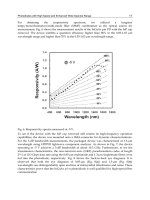
The camera sensitivity for one of the SXI cameras is given in Fig. 15(a). The Quantum
Efficiency (QE) calculated using Eq. 10 through 14 and camera gain K=7.62 electrons per
count is plotted as a function of photon energy in Fig. 15 (b). The data scatter as measured
by the standard deviation was 1% or less at each point. The dip near 1800 eV and the fall-
off after 2000 eV are properties of Si. Si that is 15 m thick transmits up to 35% as it
approaches the K edge at 1839 eV. It begins transmitting again above 2500 eV and is
transmitting 80% at 8 keV. These QE results are similar to that obtained by Poletto (1999).
There are two possible causes why the QE does not approach 1 when the photons are
completely absorbed: (1) There may be absorption at the surface coating of the Si; (2) the
Photodiodes – Communications, Bio-Sensings, Measurements and High-Energy Physics
252
Quantum Yield may be less than the photon energy divided by 3.66 eV per electron-hole
pair. Analysis of a large number of single photon events could show the relative
contribution of each effect.
6.2 Flat field
The flat field source is the 1 mm diameter spot on the anode. The anode is 1405 mm from the
CCD. This arrangement would produce a flat field within 1% if there were nothing between
the anode and the CCD. There is a light blocker that has an aluminum coating on a
polyimide film (Al 1054 Å 50 Å; polyimide 1081 Å 100 Å). This item does not affect the
flat field within the 1% cited above. The filter can cause a variation in the beam intensity
across the CCD if there is sufficient variation in thickness, foreign material, or misalignment
with the anode. A comparison of all the flat field images implies that the maximum
variation is 1% peak-to-peak.
(a) (b)
Fig. 15. The SXI (a) camera sensitivity and (b) quantum efficiency as measured by the
camera count per pixel for each photon of a given energy. The measurements made at X-ray
energies below 8800 eV were done on the Manson. The higher energy measurements were
done on the HEX.
Fig. 16(a) shows the flat field image for one of the SXI cameras at the Cu 8470 eV energy
band. The image is set at high contrast so that the pixel signal variation shows clearly. A
gross pattern is observed with the sensitivity at a maximum near the left center and
decreasing slowly going away from the maximum. The image in Fig. 16 (b) is at Ti 4620 eV;
it shows the same pattern but decreased magnitude. The pattern continues to decrease in
magnitude until it is no longer visible at 3000 eV. Vertical lineouts averaged over a small
horizontal width (see band in Fig. 16(b)) for three images at three different X-ray energies
are shown in Fig. 17. The lineouts are normalized by dividing by the maximum counts in
each image. The maximum sensitivity variation for each of the curves in Fig. 17 is 13% at
8470eV, 6% at 4620eV and 2% at 3580eV.
A flat field image of the Mg 1275 eV band is shown in Fig. 16(c) for comparison to the
higher energy flat field images. There is no trace of the sensitivity variation pattern that is
seen at higher energies. The 1275 eV lineout in Fig. 17 shows that the maximum variation is
less than 1%, which is the measurement limit of our flat field procedure.
This sensitivity variation is a large scale effect; it includes groups of pixels and is probably
related to the CCD manufacturing process. Any sensitivity variation of individual pixels is
less than the photon noise associated with averaging 10 images.
20
30
40
50
60
70
80
90
100
850 1850 2850 3850 4850 5850 6850 7850 8850
Counts/photon
Energy, eV
SXI Camera Sensitiv ity
0.0
0.1
0.2
0.3
0.4
0.5
0.6
0.7
0.8
0.9
850 2850 4850 6850 8850 10850 12850 14850
Energy, eV
SXI Quantum Efficiency
QE
Quantitative Measurements of X-Ray Intensity
253
A different phenomenon was seen at low energies. Small irregular patches having
diminished sensitivity were observed that are readily seen in Fig. 18(a). This image shows a
portion of the CCD. The effect on sensitivity in these regions also shows an energy
dependence. Fig. 8b is a similar image taken at 3080 eV. The irregular patches have now
become quite dim compared to what was observed at 1275 eV. At 4500 eV, these paths of
low sensitivity have completely disappeared.
(a) (b) (c)
Fig. 16. Flat field image for the (a) Cu anode, 8470 eV and (b) Ti anode, 4620 eV, showing the
pixel sensitivity variation (Signal range: 5200 to 7200 counts/pixel) The vertical band was
the area used to calculate the cross section that is shown in Fig. 17. The same region was
used for the cross section at the other energies. (Signal range: 5200 to 7200 counts/pixel) (c)
Flat field image for the Mg anode, 1275 eV, showing the pattern observed at the higher
energies shown in Fig. 16(a) and (b) has completely gone and the pixel sensitivity is flat.
Normalized Cross Section
0.84
0.89
0.94
0.99
1.04
100 600 1100 1600 2100
Y pixel
relative signal
1275eV
3580eV
4620eV
8470eV
Fig. 17. Normalized vertical lineouts from flat field images at several X-ray energies. The
lineouts were normalized to the maximum counts in each image. As the X-ray energy
increases, the pixel sensitivity shows a greater vatiation.
There are several possible causes for these dark regions. Debris on the CCD surface could
absorb X-rays and would be energy dependent, absorbing X-rays less as the energy
increased. Damage to the CCD would likely cause an energy dependence that would
increase the variance of the defective region from the surrounding pixels as the energy
increased. Damage to the surface coating could produce this effect if the coating were
thicker in that defective region. When we examined the CCD surface with a magnifying
glass it did appear that the coating was deformed. It looked like a manufacturing defect.
Photodiodes – Communications, Bio-Sensings, Measurements and High-Energy Physics
254
It is difficult to correct these images using the normal method of flat field inversion. This
could be done if you limit the energy range of the X-ray source. But the characterization
always provides the information necessary for the effective use of the X-ray camera.
(b) 1275 eV (a) 3080 eV
Fig. 18. These are the same sections of a flat field image taken at two different energies, (a)
1275 eV and (b) 3080 eV. The sections cover about ¼ of the entire CCD. The dark regions are
CCD surface defects causing diminished pixel sensitivity. For the 1275 eV section shown in
(a) the blemishes are much darker than in the 3080 eV image shown in (b).
6.3 Calibrating a front illuminated CCD camera from 705eV to 22keV using the Manson
and HEX sources
The SXI camera described above plays a critical role in the NIF operation, but this specific
chip is no longer manufactured. There is another chip on the market with this large array,
2kx2k, 24 μm square, and we were requested to test the chip in a standard camera. The
major concern regarding this chip was that it is front illuminated.
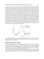
The QE measurements at X-ray energies below 10 keV were done using the Manson source
following the procedures given in 6.1. These measurements are shown in the graph of Fig.
15. Compare this to the results shown in Fig. 19 for the QE of the back illuminated camera.
The maximum QE for the front illuminated camera is QE=0.34 near 2300 eV. This is almost a
factor of 3 lower than the QE measured for the back illuminated camera. The predominant
difference begins to show below 1000 eV. At the Cu L lines, near 930 eV, the QE for the front
illuminated camera is down by a factor of 10 from the front illuminated camera. At the Fe L
lines near 705 eV, the QE is down by a factor of 100.
Fig. 19. The quantum efficiency measured for a front illuminated CCD sensor.
Quantitative Measurements of X-Ray Intensity
255
The measurements at 10 keV and lower energies were done on the Manson. The
measurements at higher energies were made using the HEX. Compare this to the QE
measurements shown in Fig. 15.
The Manson can only be used effectively up to the Cu K lines. The QE measurements at
higher energies have to be done on the HEX. The CCD cameras must be kept in a vacuum
since they are cooled and the HEX has a vacuum chamber on a rail as is seen in Fig.11. The
chamber is very similar to that shown on the Manson. It differs in having a Be window on
the side facing the Hex source. The camera is mounted on the opposite side from the Be
window. The HEX fluorescer source is near 10mm diameter rather than the “point” source
of the Manson. The X-ray beam is not flat across the entire CCD surface but is flat near the
beam center. The camera is moved horizontally and vertically until the X-ray beam is
centered on the CCD. The camera is then moved aside on the rail and the CdTe detector is
placed at the same distance from the source as was the CCD. The beam center is then
determined by moving the detector horizontally and vertically. These are the measurements
used in Eq. 10 to determine the QE shown in Fig. 15 and Fig. 19 for the higher X-ray
energies. The observation then is that the QE at these energies is the same for the front
illuminated and the back illuminated cameras.
Measuring the sensitivity variation on the HEX requires that the X-ray intensity
measurement be carefully measured over the entire area and an analytical representation be
developed. This functionality is being developed now. We will use both the CdTe detector
on a motorized X,Y positioner and image plates to measure the X-ray intensity distribution.
6.3 Single photon measurements using the Manson source
Images can be taken at sufficiently short exposure times so that most or all of the incidents
recorded by the camera are caused by individual photons. These single photon images
provide spectral information. This technique is used for astronomical measurements and
laser plasma studies. The image shown in Fig. 20(a) was taken on the Manson source using a
Ti anode and a Ti filter 100 μm thick. This is the same condition that was used to generate
the spectrum shown in Fig. 7 using an energy dispersive detector. The camera used was a
silicon CCD type having 1300 pixel x 1340 pixel array and the pixel size was 13 μm square.
A background image using the same exposure time and no X-rays has been subtracted from
the original X-ray image. The region shown in the figure is a 100 pixel square. There are
approximately 95 single photon events in this 10000 pixel area, or about a 1% fill. This is the
fill rate typically used in single photon measurements. Note that a significant fraction of the
single photon events produce counts in more than one pixel, that is, the production of
electron/hole pairs produces by the photon occurs in more than one pixel.
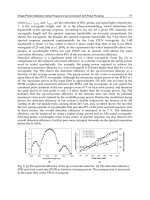
The graph shown in Fig. 20(b) is a histogram of the entire pixel array for the single photon
image of the Ti X-rays. This plot shows the number of times a pixel has a given count as a
function of counts. The histogram exhibits two peaks and they are above 400 camera counts.
The two peaks are the Ti Kα photons occurring at 415 camera counts and the Ti Kβ photons
occurring at 454 camera counts. These peaks represent single pixel events where the total
number of electron/hole pairs produced by the photon is contained within that single pixel.
As stated in the previous paragraph, there are many incidents in the image where the single
photon produces counts in multiple pixels. These multi-pixel events produce the rising
number of incidents in the graph going toward lower counts. There are no incidents at
counts above the K-M band. Compare this spectrum to that shown in Fig. 7 where an energy
Photodiodes – Communications, Bio-Sensings, Measurements and High-Energy Physics
256
dispersive Si detector was used. The spectral resolution is nearly the same for each detector.
In general then, a camera is an energy dispersive detector when operated in the single
photon mode.
(a) (b)
Fig. 20. (a) This image shows single photon incidents on a CCD camera zoomed in to show
the individual pixels in a small region of the camera active area. (b) This graph is a CCD
active area showing the Ti K-L and K-M spectral bands. Compare this to the spectral scan of
the Ti emission using the energy dispersive detector shown in Fig. 3.
The above description also describes a method for calibrating the camera count to spectral
energy. As described earlier for the camera efficiency calibration, images are taken with
several anode/filter combinations. The camera count for the peak center is then plotted
against the literature value for the spectral energy (more precisely, a weighted average of
the unresolved spectral lines).
More sophisticated software than a simple histogram can be devised that would capture a
large portion of the multi-pixel incidents that are single photon events. This would reduce
the noise that is seen in the histogram peaks. The method requires identifying significant
pixels by a thresholding technique, then adding the counts of adjacent pixels to the central
pixel. This represents a new image that generates a new histogram. The spectral peaks will
be better defined because the noise is reduced.
6.4 Characterizing and calibrating an uncooled X-ray CID camera using the HEX
source
This section describes the characterization of a CID camera that was planned as the detector
in a spectrometer system that was to be used on the LLNL NIF target chamber. The initial
interest was to measure the emission from highly ionized Ge so the camera was
characterized in the 10 keV region using the HEX source (Carbone, 1998 and Marshall,
2001). The fluorescers chosen were Cu, Ge, and Rb giving weighted average for the K-L and
K-M transitions of 8.13 keV, 10.01 keV, and 13.58 keV respectively.
The major use for this CID sensor is for dental X-rays. It is relatively cheap and therefore
expendable, a desirable property for the NIF application. The camera operates at room
temperature normally, which gave a challenging problem to the characterization on HEX.
Since the CID operates at room temperature, the dark current can saturate the camera for
exposure times less than 10 seconds. This not a problem on NIF since the exposure time can
be less than 1 second with sufficient X-rays to provide a bright spectral image.
Quantitative Measurements of X-Ray Intensity
257
As indicated in the earlier description of CCD camera calibrations on the HEX, minutes of
exposure time are needed to get a satisfactory signal. Preliminary experiments with the CID
camera showed that we would be limited to three-second exposure times. It was determined
that multiple exposures, on the order of 100 exposures, would be needed to obtain
satisfactory photon statistics. The multiple exposures would also allow us to average the
readout noise and get to the limit that photon statistics were dominant. A shutter control
system was implemented for automatically taking the multiple images. We quickly found
that drift in the dark current required us to take background images immediately after the
X-ray exposure. The system was designed so that an image was taken with the shutter open
to the X-rays, then the next image was taken with the shutter closed. In this way a pair of
images were produced, one image exposed to X-rays and the other as a background, that
were close enough in time that there was no observable dark current drift. A black Kapton
sheet, 50 μm thick, was used to shield the camera from visible light. The same type shield is
used for the camera on the NIF target chamber.
The X-ray beam was characterized geometrically using image plates to optimize collimator
and distance choices. The intensity distribution was measured using the CdTe energy
dispersive detector at multiple locations across the beam. Multiple images were taken with
the CID, and then the detector was placed at the same location as the center of the CID had
been located to verify that there was no drift in the X-ray source intensity. The multiple
images were analyzed by subtracting each background from the previously taken X-ray
image and summing the 100 resulting images. The final image then was effectively a 300
second exposure with the background removed. The measurements concentrated on the
X-ray beam center for this initial effort. The CID camera efficiency, counts per pixel per
photon, could then be calculated using the CdTe intensity measurements.
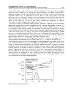
The results are shown in Fig. 21. The camera response was measured for two CID cameras at
three spectral energies over the range of interest. The responses of the two cameras are the
same within the experimental uncertainty. The expected response was modeled using the
vendor’s specification for camera gain and Si thickness and a typical surface coating. This is
shown by the blue line in the figure. This did not fit the measurement data so a second
model curve is shown using a thinner Si effective thickness.
The CID camera is now considered to be suitable for the spectrometer operation. The
spectrometers will be incorporated as part of existing diagnostics at several locations on the
NIF target chamber. All cameras will be calibrated using an extension of the procedure. It
will extend to lower X-ray energies using the Manson source and measure the sensitivity
variation of the CID over the full pixel array.
7. Conclusion
The chapter started with a presentation of basic X-ray physics needed to follow the
description of X-ray detector calibration. The X-ray sources used at NSTec for calibrating
detectors were described. The operation and characteristics of solid state semiconductor
detectors was presented. Single sensor photodiodes, both current detectors and pulse
counters, are used to measure the X-ray source beam intensities. The detectors are calibrated
using either of 2 procedures: radioactive sources that are NIST traceable; a synchrotron
beam that has an internationally accepted beam intensity accuracy. The chapter presented
the methods used and the results obtained for calibrating several types of X-ray cameras.
Photodiodes – Communications, Bio-Sensings, Measurements and High-Energy Physics
258
The accreditation procedure for recognition of the X-ray calibration labs as certified to
international standards is in process. This requires the full analysis of all uncertainties
associated with the detector calibration. The calibrated photodiode has yet to be completed
for the synchrotron calibration. It will then be used to better fill the efficiency curves of the
energy dispersive photodiodes. There are several agencies around the world that oversee
and certify the accreditation. NSTec will be working with one of them to achieve
certification. The NSTec X-ray labs will continually improve existing procedures and
develop new methods for calibrating X-ray detection systems and components.
0.0
2.0
4.0
6.0
8.0
10.0
12.0
0 5 10 15
counts per pixel per photon
Energy, keV
Camera Response
model 7um
model 5um
camera A response
camera B response
Fig. 21. The measurement results for the CID camera efficiency are shown as the crosses and
the plus signs. The curves are model calculations for the CID camera response based on
camera characteristics described in the text.
8. Acknowledgment
This manuscript has been authored by National Security Technologies, LLC, under Contract
No. DE-AC52-06NA25946 with the U.S. Department of Energy. The United States
Government and the publisher, by accepting the article for publication, acknowledges that
the United States Government retains a non-exclusive, paid-up, irrevocable, world-wide
license to publish or reproduce the published form of this manuscript, or allow others to do
so, for United States Government purposes. This manuscript was done under the auspices of
the U.S. Department of Energy by Lawrence Livermore National Laboratory under Contract
DE-AC52-07NA27344.
Quantitative Measurements of X-Ray Intensity
259
There were many persons from both NSTec and LLNL involved in developing the X-ray
laboratory calibration methods. I particularly thank Susan Cyr for special effort in putting
this manuscript together.
9. References
American Association of Physicists in Medicine (AAPM) (2006). Report No. 93, Acceptance
Testing and Quality Control of Photostimulable Storage Phosphor Imaging
Systems, available from
Carbone, J., Zulfiquar, A., Borman, C., Czebiniak, S., & Ziegler, H. (1998). Large format CID
x-ray image sensors, Proceedings of SPIE 3301, 90 doi:10.1117/12.304550, Solid
State Sensor Arrays: Development and Applications II
Center for X-Ray Optics (CXRO) (n.d.). X-ray interactions with Matter, available from
ESTAR Program (n.d.). Available from
Gottwald, A., Kroth, U., Krumrey, M., Richter, M., Scholze, F., & Ulm, G. (2006). The PTB
high accuracy spectral responsivity scale in the VUV and x-ray range, Metrologia
43
Haugh, M. J. and Stewart, R. (2010). Measuring Curved Crystal Performance for a High
Resolution Imaging X-ray Spectrometer, Hindawi Publishing
Haugh, M.J. & Stewart, R. (2010). X-Ray Optics and Instrumentation, Article ID 583620
Herzberg, G. (1945). Atomic Spectra and Atomic Structure, Dover
International Radiation Detectors (IRD) (n.d.). Available from
Janesick, J. (2000). Scientific Charge-Coupled Devices, SPIE Press, Bellingham, WA
Knoll, G. F. (2001). Radiation Detection and Measurement, 3
rd
edition, John Wiley & Sons
Maddox, B. et al (2011). High-energy backlighter spectrum measurements using calibrated
image plates, RSI 82, 023111
Marshall, F. J., Ohki, T., McInnis, D., Ninkov, Z., Carbone, J. (2001). Imaging of laser–plasma
x-ray emission with charge-injection devices, Rev. Sci. Instru. 72 713
Poletto, L., Boscolo, A., & Tondello, G. (1999), Characterization of a Charge-coupled
Detector in the 1100-0.14 nm (1 eV to 9 keV) Spectral Range, Applied Optics, 38, 1 Jan
99
Physikalisch-Technische Bundensanstalt (PTB) (n.d.). available at
Podgorsak, E. (2010). Radiation Physics for Medical Physicists 2
nd
edition, Springer
Quaranta, C., Canali, G., Ottavani, G. , & Zanio, K. (1969). Electron-hole Pair
Ionization Energy in CdTe between 85K and 350K, Lettere Al Nuovo Dimento, 4,
p. 908-910
Schneider, M.B., Jones, O.S., Meezan, N.B. et al (2010). Images of lthe laser entrance hole
from the static X-ray imager at NIF, Rev. Sci. Instru. 81 10E538.
Stepanov, S. (1997). X-ray Server, available from
Photodiodes – Communications, Bio-Sensings, Measurements and High-Energy Physics
260
Stepanov, S. (2009). X0h Program, avalable from
Nicola D’Ascenzo and Valeri Saveliev
National Research Nuclear University
Russia
1. Introduction
One of the main methods for the detection of the energy of the elementary particles is the
conversion of the particle energy into light photons due to the scintillation process and then
the conversion of the light photons into the electronic signal due to the photoelectric process
(Scintillator/Photo-detector Detection Systems). These detection systems are widely used in
high energy physics and currently operated in running experiments, as for example in the
CDF experiment at Tevatron (CDFII, 1996) and in the ATLAS experiment at Large Hadron
Collider (ATLAS, 1999). The same method is implemented in Nuclear Medicine and is
widely used in clinical practice. Detection systems for Positron Emission Tomography (PET),
Single-PET and Gamma Camera are based on scintillators read out by photo-detectors.
The main requirement of such applications is the necessity of the detection of a low photon
flux. A typical number of scintillation photons produced by modern scintillating crystals is
about 25 photons/keV and about 1 photon/keV is generated by a plastic organic scintillator.
For a long time the main photo-detector for such detection systems was the Photomultiplier
Tube (PMT), which was created more than 50 years ago and has many well known
disadvantages (Toshikaza et al., 2006).
As alternatives to the PMTs, in the last decade, a new type of photo-detector was developed
on the basis of the semiconductor technology, the Silicon Photomultiplier (SiPM) (Golovin
& Saveliev, 2004; 2000). At the present time such devices are produced by few companies
as Multi Pixel Photon C ounters (MPPC), Hamamatsu, Japan (Yamamura, 2009), S ensL,
Ireland (SensL, 2010)
The SiPM consists of an array of space-distributed micro sensors. Each micro sensor is capable
of detecting a single quantum of light - the array is detecting the photon flux. This innovative
detecting structure is a great technological improvement in the efficient detection of low
photon fluxes. The SiPM is r apidly being used and proposed in many experimental physics
and nuclear medicine applications. Few examples give the impression of the extension
of use of such detectors: read-out of the fiber/scintillator detectors in the neutrino T2K
experiment (Yokoyama, 2009), calorimeter systems at the International Linear Collider (ILD,
2009), CMS hadron calorimeter at the Large Hadron Collider (Freeman, 2009) and others.
Many projects are active on the design of PET and Gamma camera using SiPM-crystal
detectors (Herbert, 2006).
The aim of this chapter i s to show the advantages of using t he SiPM for the low photon fluxes
detection in scintillator-based high energy physics and medical applications. The examples
The New Photo-Detectors for High Energy
Physics and Nuclear Medicine
13
2 Will-be-set-by-IN-TECH
(a) (b)
Fig. 1. Schematic of the avalanche process ( a) and schematic of t he avalanche breakdown
micro-cell of a Silicon Photomultiplier n on p type with virtual guard ring (Saveliev, 2010).
of the hadron calorimetry at the International Linear Collider and the new generation PET
are considered and the potential of the interplay between mathematical modelling and
experimental study is analysed in the design and optimization of such applications.
2. The Silicon Photomultiplier
2.1 Photo-detector structure
The SiPM is a semiconductor-based photo-detector developed for the detection of low photon
fluxes. It consists of an array of micro-sensors (microcells), which are designed to detect
a single quantum of light with high efficiency. They are based on a special geometry
pn juntion (Golovin & Saveliev, 2004). Under a reverse bias a depleted area with a high
in-built electric field is formed inside the structure. The interaction of a visible photon in
the depleted area is mediated through the photo-electric effect with the consequent creation
of one electron-hole (e/h) pair. The detection of such small signal is a general problem due
to the thermal noise of the detector itself and of the front-end electronics (Alvares-Gaume,
2008). The SiPM has the possibility of the detection of a single photon or single e/h pair
through a very high intrinsic gain of the order of 10
6
. The amplification is achieved by
the avalanche breakdown process due to secondary impact ionization (Tsang, 1985). The
schematics of the amplification process in one microcell of the SiPM is shown in Fig. 1a.
When the e/h pair is created by a photon interaction, as in the figure, both the generated
electron and hole are accelerated in the electric field and reach an energy higher than the
ionization energy of the valence electrons and holes in the semiconductor. This initiates a
self-sustaining avalanche process. The current rises exponentially with time and reaches the
breakdown condition. The avalanche process is stopped via a quenching mechanism obtained
by a serial resistor to every microcell. The rising current flows out from the microcell through
a q uenching resistor causing a voltage drop on the resistor and accordingly to the pn junction
bias voltage. When the build-in electric field is lowered enough, the aval anche stops. After the
quenching, a hold-off time is required to the microcell in order to restore the proper build-in
electric field. The resulting intrinsic gain of the microcell is about 10
6
electrons per detected
photon, which is well above the noise level of modern measurement electronics. A structure
of the Silicon Avalanche Breakdown micro-cell is shown in Fig. 1b. The structure consists of
a silicon substrate with a p-type epitaxial layer (epi). The avalanche breakdown structure
262
Photodiodes – Communications, Bio-Sensings, Measurements and High-Energy Physics
The New Photo-detectors for High Energy Physics and Nuclear Medicine 3
Fig. 2. Equivalent schematic of the structure of the Silicon Photomultiplier (Saveliev, 2010).
(a) (b)
Fig. 3. Micro image of a modern Silicon Photomultiplier. Overall view 1 ×1mm
2
(a) and
detailed v iew of the microcell area (b) (Saveliev, 2010) .
is represented by the shallow pn junction (n
+
p) in the silicon epitaxial layer with the so
called virtual guard ring designed to prevent peripheral avalanche breakdown processes. The
heavily doped n
+
region is connected to one electrode through a serial quenching resistor.
The second electrode is formed on the back side of the substrate. The pn junction is designed
to reach a v ery high in-build electric field of the order of 10
5
V/cm within the small thickness
of the silicon layer of the order of few microns.
The schematic structure of the modern SiPM is shown in Fig. 2. It consists of an array of the
above described pn junctions micro-cells (light grey squares) of typical size 30
× 30 μm
2
on
a total sensitive area of few mm
2
. Each microcell has the quenching element located close
to the pn junction (grey and marked as Q element). The microcells are connected in parallel
through a common electrode. The sum of signals from the array provides an output signal
proportional to the number of detected photons.
The topology of the SiPM is shown on Fig. 3. On Fig. 3a is shown the top view of 1 mm
2
SiPM with micro-cells size about 30 × 30 μm
2
. The total number of micro-cells is 1000 on
1mm
2
. The typical size of Silicon Photomultipliers is 1 × 1mm
2
(up to 5 ×5mm
2
without
significant degradations in performances). In Fig. 3b is presented the microscopic view of a
single avalanche breakdown micro-cell where the main elements of the structure are visible:
the sensitive area (1), the quenching element (2), a part of the common electrode system (3).
The microcells are also optically isolated i n order to reduce the probability that optical photons
263
The New Photo-Detectors for High Energy Physics and Nuclear Medicine
4 Will-be-set-by-IN-TECH
Fig. 4. Spectrum of a low photon flux signal in a SiPM.
produced in the avalanche process initiate an avalanche in neighbouring cells. The optical
trenches around each microcell are also visible in the figure.
2.2 Silicon Photomultiplier performance
2.2.1 Single photon detection
The most challenging characteristic of the photo-detectors is the possibility of excellent single
photon detection performance. The spectrum of a low photon flux detected with a SiPM
is shown in Fig 4. The measurement is performed at room temperature. The resolution
of the SiPM allows a precise analysis of the detected photon flux. The structure of the
spectrum shows well defined peaks corresponding to the number of detected photons. The
first peak corresponds to the noise of the measurement electronics (pedestal). The s econd
peak corresponds to one photon detected, the third peak corresponds to two photons detected
and so on. The typical Poisson distribution characterizing the photon statistic describes the
spectrum. The SiPM introduces a significant improvement in the possibility of single photon
detection in comparison with the traditional photomultiplier tubes (Toshikaza et al ., 2006).
2.2.2 Photon detection efficiency of SiPM
The photon detection efficiency (PDE) of the Silicon Photomultiplier could be defined as:
PDE
= η(λ) · P
b
(V) · F (1)
where η
(λ) is the quantum efficiency of the Silicon microcell structure, P
b
(V) is the probability
of the avalanche breakdown in the silicon microcell structure, F is the filling factor of structure
geometry (Saveliev, 2010).
The experimental determination of the photon detection efficiency of the SiPM is usually
performed in two steps. First the photo detection probability of a single micro cell is measured
relative to a calibrated photo detector with a monochromator light source. Then the result is
rescaled to a full area SiPM multiplying by the filling factor, which in modern technologies is
within the range 0.6–0.8.
The measured photon detection efficiency of the SiPM is shown in Fig. 5 as a function of the
wavelength at 2V above the breakdown voltage. The PDE reaches a peak value of abo ut 20%
at aro und 500 nm. The quantum e fficiency of photocathodes used in PMT shows a maximum
264
Photodiodes – Communications, Bio-Sensings, Measurements and High-Energy Physics
The New Photo-detectors for High Energy Physics and Nuclear Medicine 5
Fig. 5. Photon detection efficiency of the SiPM (black dots) Stewart (2008). Spectra o f
photo-luminescence (blue dotted line) and radio-luminescence (red continuous line) of a LSO
crystal (Mao, 2008).
of 20-30 % within a spectral region between 350 nm and 500 nm (Toshikaza et al., 2006).
Improvements are ongoing in the SiPM technology in order to achieve a high photon detection
efficiency including the increasing the sensitivity in the blue spectral region. A realistic value
of the photon detection efficiency of modern SiPM is 40
−60%.
In the same Fig. 5 the photo-luminescence and radio-luminescence emission spectra of LSO
are shown according to the reported experimental measurements (Mao, 2008). It is observed
that the peak of the emission spectrum is 420 nm for the photo-luminescence and 450 nm for
the radio-luminescence. The red shift of the radio-luminescence spectrum is probably due to a
higher contribution of the irregular luminescence centre Ce2. The photon detection efficiency
of the SiPM matches the requirements for the read-out of the scintillation light from LSO.
2.2.3 Time performance of SiPM
The time performance of the SiPM is defined by two factors: the rising time of the avalanche
breakdown signal and the recovery time, which is defined by the process of reconstruction
of the pn junction state after quenching the avalanche breakdown process and recharging
through the quenching resistor. The rising time is defined by the generation time of the
avalanche breakdown process and is characterized by the drift time of carriers under the
high electric field. The drift velocity of the carriers under electric field of about 10
5
V/cm
is limited by the scattering process and in silicon structures it is approximately 10
7
cm× s
−1
.
As an example for the thickness of a depleted area of 4 microns the rising time is about 30
ps (Saveliev, 2010). The time resolution of the SiPM is measured as 27.54 ps, including the
response of measurement system (Stewart, 2008).
2.2.4 Dynamic range and linearity of SiPM
The detection of photons by a silicon Photomultiplier is a statistical process based on
the probability of d etecting randomly space-distributed photons by the limited number of
space-distributed sensitive elements. The photon detection efficiency and the total number
of micro-cells determine the dynamic range of the Silicon Photomultiplier. The number
265
The New Photo-Detectors for High Energy Physics and Nuclear Medicine
6 Will-be-set-by-IN-TECH
of detected photons n
dph
(number of micro-cells with signal) as function of the number of
incident photons can be approximated by the following expression:
n
dph
= N
mic
1
−e
−
PDE·N
ph
N
mc
(2)
where N
mc
is the total number o f microcells, N
ph
is the number of incident photons and PDE
is the photon d etection efficiency.
The Silicon Photomultiplier response is linear when the number of incident photons is much
less than the total number of micro-cells. The Silicon Photomultiplier response begins to
saturate when the number of fired pixels reaches approximately a quarter of the total number
of micro-cells, but could be corrected by well k nown statistical functions (Saveliev, 2010) .
2.2.5 Dark rate of SiPM
One of the main factors limiting the performance of the Silicon Photomultiplier is the dark
rate. The dark rate is the frequency of a thermal e/h pair created in the sensitive area of the
SiPM. Such e/h pair generates an output signal with amplitude equivalent of a single photon
signal and could not distinguished from it. The typical dark rate value for the modern Silicon
Photomultipliers is in the range 0.1-1 MHz per mm
2
(Saveliev, 2010).
The amplitude of the dark rate pulses is equivalent to the single photon signal amplitude and
in applications dealing with tens-hundred of photons it could be neglected. For applications
with very low photon flux the average dark rate can be measured and subtracted. However,
the statistical variation in the dark rate cannot be subtracted and constitutes a noise source that
determines the minimum detectable signal. As the dark rate of the Silicon Photomultiplier
scales as its area and the acceptable dark rate is about 10
6
in low photon flux, the maximum
designable area is limited to around few mm
2
.
3. Recent advances of scintillator/SiPM detection systems in high energy physics
3.1 The scintillator/SiPM detection system for hi ghly granular hadron calorimetry
A modern concept of high energy physics detection systems is the particle flow algorithm
(PFA) (Thompson, 2007). This method is proposed for the experiment at International Linear
Collider (ILD, 2009). Instead of performing a pure calorimetric measurement, as in traditional
environments, the reconstruction of the four vectors of all the observable particles in the jet is
proposed. The reconstructed jet energy is the sum of the energy of the individual particles.
The momentum of the charged particles is measured in the tracker, while the energy of the
neutral particles is measured in the calorimeters. The electromagnetic calorimeter is used for
the measurement o f the energy of photons and for the identification of photons and electrons.
The hadronic calorimeter is used for the measurement of the energy of neutral hadrons and
for the identification of hadrons. The muon chambers are used for the identification of muons.
A detector optimized for the particle flow should have an excellent separation power of the
components of the jets. The most important features in this respect are the spatial separation
of the particles in the high energy jets, which is achieved with a high magnetic field, and
high space resolution systems including the calorimeter systems. The key point of the hadron
calorimetry designed for the p article flow technique is the granularity. It allows in fact
to identify the single particles through the morphological properties of the shower. The
calorimeter becomes an imaging device more than an energy measurement device.
Mathematical modelling studies were performed for the optimization of the performances of
266
Photodiodes – Communications, Bio-Sensings, Measurements and High-Energy Physics
The New Photo-detectors for High Energy Physics and Nuclear Medicine 7
Fig. 6. Design of the scintillator/SiPM detection system for hadron calorimetry. The green
sensitive SiPM is coupled to the scintillator through a wavelength shifter fiber (CALICE,
2010).
the hadron calorimeter for the International Linear Collider. It is shown that a transverse
segmentation of 3
× 3cm
2
and a longitudinal segmentation of about 1 cm satisfies the
requirements in the experiment. Such modern performance calorimeter system, especially
the hadron calorimeter, could be developed only o n the basis of new t echnologies (ILD, 2009).
One of the solutions i s to use the modern scintillator/SiPM detection system.
The first proposed design of the scintillator/SiPM detection system consists of a 3
× 3 ×
0.5 cm
3
plastic organic scintillator tile read-out individually by a Silicon Photomultiplier
(Fig. 6). The coupling between the scintillator and the photo-detector is performed via a
wavelength shifter fiber. The scintillator/photo-detector system was optimized to yield about
15 photons on average in response to a minimum ionizing particle.
A simplification of the coupling between SiPM ad scintillator would be highly desirable, in
order to extend the concept to a large scale detector. The new generation of SiPMs produced by
Hamamatsu (MPPC) shows a better optical sensitivity in the 420 nm spectral region, making
it possible to investigate the direct read-out of the scintillation tile (D’Ascenzo et al., 2007).
3.2 Mathematical model of a highly granular calorimeter based on scintillator/SiPM with
individual read-out
In order to estimate and optimize the performance of the detection system with SiPM, a
mathematical model of a scintillator/SiPM calorimeter is performed on the basis of the
GEANT4 simulation framework. It allows to include the geometry and the physics processes
in response to any final states resulting from the studied high energy particle collisions.
The result of the simulation has maximal flexibility and can be studied with the same
reconstruction and statistical analysis techniques developed for the application to real data.
The mathematical model includes a detailed geometrical description of the full detector
system. The components of the mathematical model are shown in Fig. 7. In the barrel
region the detector components are the vertex detectors (VTX, SIT), the tracker (TPC, SET),
the electromagnetic and hadronic calorimeters (ECAL, HCAL) and the return yoke with
muon system (YOKE). In the forward region the forward tracking detectors (FTD, ETD) the
luminosity (LCAL, LHCAL) and veto d etectors (BCAL) are included.
267
The New Photo-Detectors for High Energy Physics and Nuclear Medicine
8 Will-be-set-by-IN-TECH
Fig. 7. Mathematical model of the detector for the International Linear Collider. The
overview of the detector components is shown. From the inside to the outside, the detector
components are the vertex detectors (VTX, SIT), the tracker (TPC, SET), the electromagnetic
and hadronic calorimeters (ECAL, HCAL) and the return yoke with muon system (YOKE). In
the forward region the forward tr acking detectors (FTD, ETD) the luminosity (LCAL,
LHCAL) and veto d etectors (BCAL) are included (ILD, 2009).
The hadronic calorimeter co nsists o f one barrel and two end-cap modules. The barrel module
has octagonal shape with inner and outer radius respectively of 2.02 m and 3.33 m. The end
cap modules has also octagonal shape and has a longitudinal thickness of 1.3 m, inner and
outer radius of 329 cm and 3.33 m. Each module is composed of 40 layers in an alternating
structure of 0.5 cm thick plastic scintillators as active material and 1 cm thick stainless steel as
absorber.
The detailed geometry of the scintillator/SiPM detection system is introduced in the
simulation. Each scintillator layer is segmented in 3
× 3cm
2
scintillator tiles, individually
read out by a SiPM. The total amount of calorimeter cells is about 10
6
. The energy deposited
in each cell is independently calculated and stored for further analysis.
The response of the scintillator/SiPM detection system is introduced with a parametric
model based on the results of the experimental study of the hadron calorimeter system
prototype ( CALICE, 2010).
The detector is immersed in a magnetic field of 3.5 T.
The reconstruction of the particles in the final state from the simulated detector response is
performed with a reconstruction software based on the Particle Flow Algorithm.
The dependence of the jet energy resolution on the size of the sensitive cells of the hadronic
calorimeter is shown in Fig. 8. The energy resolution of jets with energy as low as 45 GeV
is independent from the size of the HCAL cell, while higher energetic jets show a stronger
dependence on the granularity of the hadronic calorimeter. This effect is due to the increased
complication of the structures in the hadronic calorimeter in response to higher energy jets.
268
Photodiodes – Communications, Bio-Sensings, Measurements and High-Energy Physics
The New Photo-detectors for High Energy Physics and Nuclear Medicine 9
Fig. 8. Monte Carlo e stimation of the dependence of the jet energy resolution on the sensitive
element size of the highly granular hadronic calorimeter based on scintillator/SiPM
detection system with individual re ad-out (ILD, 2009).
Consequently the best possible granularity is needed in order to identify each contribution.
The result indicates that the ILC jet energy resolution goal is achieved with a 3
× 3cm
2
scintillator tile segmentation (ILD, 2009).
3.3 Experimental study of the prototype of the highly granular hadron calorimeter based on
scintillator/SiPM with individual read-out
The experimental study of the new detection system on the bas is of s cintillator/SiPM
photo-detectors for application in highly granular hadron calorimeters was performed on a
prototype of hadron calorimeter. The prototype consists of a sampling structure alternating
2 cm thick absorber steel plates with 0.5 cm thick sensitive layers. It has a total surface of
90
×90 cm
2
and consists of 38 layers, for a total length of 5 λ
0
.
Each sensitive layer is a array of 216 scintillators. The 30
× 30 cm
2
core has a granularity
of 3
× 3cm
2
and the outer region is equipped with tiles of increasing size — 6 ×6cm
2
and
12
×12 cm
2
. Each scintillation tile is read-out individually by a SiPM (Fig. 6). The coupling
between the scintillator and the photo-detector is performed via a wavelength shifter fibre arc
(Kurakay WLS fiber Y11(200)). The fibre is inserted in a groove carved directly in the tile. A
mirror is placed on one side of the tile in order to minimize the light losses along the fibre.
The photo detector is installed directly on the tile coupled to a WLS fiber. A 3M reflector foil
is applied on the surface of the tiles. The sensitive layer is housed in a steel cassette, with
2 cm thick rear and front plates. The calibration o f the photo-detectors with light i s done with
a LED/clear fibre system. The fibres are embedded with the sensitive cassette itself and a
proper electronic board controls the LED s ystem (CALICE, 2010).
The electronic read-out of the signals of the Silicon Photomultipliers is made by the
special electronics ILC-SiPM chip with 18 channels, e ach composed of a variable-gain,
269
The New Photo-Detectors for High Energy Physics and Nuclear Medicine
10 Will-be-set-by-IN-TECH
Fig. 9. Set-up of the detectors in the CERN test beam. The AHCAL was te sted in combination
with a prototype of highly granular Silicon/Tungsten electromagnetic calorimeter (ECAL)
and a strip-scintillator/steel Muon Tracker Tail Catcher (TCMT) (Behnke, 2007).
Fig. 10. Pion shower ( 12 GeV) identified in the data (CALICE, 2010) .
charge-sensitive amplifier, a var iable shaper, track and hold s tage and a multiplexing
unit (Blin, 2006).
The analog hadron calorimeter (AHCAL) was tested in combination with the prototypes of the
highly granular silicon-tungsten electromagnetic calorimeter (ECAL) and of the scintillator
strip tail catcher (TCMT) at the H6 beam line of the CERN SPS facility. The experimental
270
Photodiodes – Communications, Bio-Sensings, Measurements and High-Energy Physics