Organic Light Emitting Diode Material Process and Devices Part 6 ppt
Bạn đang xem bản rút gọn của tài liệu. Xem và tải ngay bản đầy đủ của tài liệu tại đây (2.06 MB, 25 trang )
Organic Light Emitting Diode – Material, Process and Devices
116
PHOLEDs is very broad and hole trapping is not so severe. The EL emission spectra of devices
D, E, and F are shown in Fig. 12(a) and CIE coordinates in Fig. 12(b).
Fig. 10. Normalized electroluminescent spectra of devices A, B, and C at the luminance of
1000 cd/m
2
.
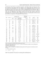
Thickness (Å)
Device D Device E Device F
X (nm) 0 10 20
Bebq
2
:Ir(piq)
3
100 100 100
Bebq
2
400 300 200
Table 6. Recombination zone position in Device C from the HTL/EML interface
Fig. 11. Recombination zone position in Device C
High Efficiency Red Phosphorescent Organic Light-Emitting Diodes with Simple Structure
117
Fig. 12. (a) EL emission spectra, and (b) CIE coordinates of devices D, E, and F.
4.2 Conclusions
A narrow band-gap host material, Bebq
2
, for red PHOLEDs with a very small exchange
energy value of 0.2 eV between singlet and triplet states has been demonstrated. It shows
almost no barrier to injection of charge carriers and charge trapping issue in PHOLEDs is
minimized. High current and power efficiency values of 9.66 cd/A and 6.90 lm/W in bi-
layered simple structure PHOLEDs are obtained, respectively. The operating voltage of bi-
layered PHOLEDs at a luminance of 1000 cd/m
2
was 4.5 V. In conclusion, simple bilayerd
red emitting device with Bebq
2
host could be a promising way to achieve efficient,
economical, and ease manufacturing process, important for display and lighting production.
5. Single layer structure
5.1 Introduction
Organic light emitting devices (OLEDs) have made significant stride (Pfeiffer et al., 2002)
and the technology has already been commercialized to mobile flat panel display
applications. Thermal evaporation technique and complicated fabrication process consisting
of multiple layers for charge carriers balancing and exciton confinement (Baldo and Forrest,
2002; Coushi et al., 2004; Tanaka et al., 2007) are employed in highly efficient
phosphorescent OLEDs. In order to overcome such complex device architecture, many good
approaches are enduring until now. High efficiency devices with pure organic bilayered
OLEDs have been reported by several researchers (Jeon et al., 2008b; Pode et al., 2009; Park
et al., 2008; Meyer et al., 2007; Z. W. Liu et al., 2009). Furthermore, bilayered devices
consisting of an organic single layer with a buffer layer on the electrode have also been
reported without any significant improvement of the device performances (Q. Huang et al.,
2002; Gao et al., 2003; Wang et al., 2006; Tse et al., 2007). However, truly organic single
layered approach is almost rare. To date, only an exclusive article on the red emitting
PHOLED single layer device with a tris[1-phenylisoqunolinato-C2,N]iridium (III) (Ir(piq)
3
)
(21 wt%) doped in TPBi (100 nm) with low values of current and power efficiencies under
3.7 cd/A and 3.2 lm/W at 1 cd/m
2
have been reported, respectively (Z. Liu et al., 2009).
In this section, we have presented efficient and simple red PHOLEDs with only single
organic layer using thermal evaporation technique. The key to the simplification is the direct
Organic Light Emitting Diode – Material, Process and Devices
118
injection of holes and electrons into the mixed host materials through electrodes. In
conventional OLEDs, usually the Fermi energy gap between cathode ( 2.9 eV) and surface
treated anode ( 5.1 eV) is about 2.0~2.2 eV which is close to the red light emission energy
(1.9 2.0 eV). As a consequence, red devices do not at all require any charge injection and
transporter layer if the host material has proper HOMO and LUMO energy levels. However,
such host materials are very rare. The most suitable option to address such issues is to
employ the mixed host system to adequately match the energy levels between emitting host
and electrodes. Mixed host system of electron and hole transporting materials to inject
electrons and holes from electrodes into the organic layer without any barrier has been
studied, respectively and employed for the charge balance. Thus, hole type host materials are
required to have HOMO energy levels at 5.1~5.4 eV to match with the Fermi energy of surface
treated ITO (5.1 eV). While 2.8~3.0 eV LUMO energy levels of electron transporting host
materials are necessary to match the Fermi level of cathode. 4,4’,4”-Tris(N-3-methylphenyl-N-
phenyl-amino)triphenylamine(m-MTDATA) and N,N’-diphenyl-N,N’-bis(1,1’-biphenyl)-4,4’-
diamine (α-NPB) were used as the hole transporting host materials. Bis(10-
hydroxybenzo[h]quinolinato)beryllium (Bebq
2
) with 2.8 eV LUMO energy was used as the
electron transport host material and Ir(piq)
3
was employed as a red phosphorescent guest.
5.2 Experimental
m-MTDATA and α-NPB as hole transporting host materials, Bebq
2
as an electron
transporting host material, and Ir(piq)
3
as a red dopant were obtained from Gracel
Corporation. Details of the fabrication process have been discussed section 3. The emitting
area of PHOLED was 2 mm
2
for all the samples studied in the present work.
5.3 Results & discussion
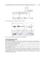
Figure 13 shows the energy band-diagram of the single layer red PHOLEDs used in the
present work. For the evaluation of single layer with different mixed host systems, the
following devices were fabricated:
Device A: ITO/m-MTDATA:Bebq
2
: Ir(piq)
3
[1~4 wt%, 100 nm]/LiF (0.5 nm)/Al (100 nm),
and Device B: ITO/α-NPB:Bebq
2
: Ir(piq)
3
[1~4 wt%, 100 nm]/LiF (0.5 nm)/Al (100 nm).
Fig. 13. Energy band-diagram of the single layer red PHOLEDs.
High Efficiency Red Phosphorescent Organic Light-Emitting Diodes with Simple Structure
119
The ratio of the hole and electron transporting hosts was fixed to 1:1. The doping
concentrations were varied from 1% to 4% to optimize the device performance. Table 7 shows
the performance of red PHOLEDs devices comprising a single emitting layer. The current and
power efficiencies values of 7.44 cd/A, and 3.43 lm/W at 1000 cd/m
2
brightness value are
reported in 4wt% doped device A, respectively. The driving voltage (to reach 1000 cd/m
2
) is
6.9 V. Very similar device performances are obtained in 2 wt% doped device A. The optimum
doping condition for Device A seems to be 4 wt% as the highest efficiency is observed at an
acceptable brightness value (1000 cd/m
2
). Whereas, the driving voltage, current and power
efficiencies values of 5.4 V, 9.02 cd/A, and 5.25 lm/W at brightness value of 1000 cd/m
2
are
reported in device B with 1 wt% of optimum doping condition, respectively. Maximum
current efficiency values for devices A and B were appeared in 4 and 1 wt% of Ir(piq)
3
doped
mixed hosts, respectively. The color coordinates are (0.66, 0.33) or (0.67, 0.32) for all devices.
Even in 1% doped device, a good red emission color is observed.
Device A Device B
1%
Doping
2%
Doping
4% Doping
1%
Doping
2% Doping
4% Doping
Turn on voltage
(@ 1cd/m
2
)
2.5 V
2.4 V
2.3 V
2.4 V
2.4 V
2.4V
Operating
voltage
(@ 1000 cd/m
2
)
7.2 V
7.1 V
6.9 V
5.4 V
5.4 V
5.3 V
Maximum
current and
power
efficiency
8.12 cd/A
7.84
lm/W
8.19 cd/A
9.86
lm/W
8.04 cd/A
10.96
lm/W
9.44 cd/A
10.62
lm/W
8.36 cd/A
9.82 lm/W
7.04 cd/A
8.11 lm/W
current and
power
efficiency
(@ 1000 cd/m
2
)
7.28 cd/A
3.18
lm/W
7.34 cd/A
3.29
lm/W
7.44 cd/A
3.43 lm/W
9.02 cd/A
5.25
lm/W
8.26 cd/A
4.80 lm/W
7.04 cd/A
4.10 lm/W
CIE (x, y)
(@ 1000 cd/m
2
)
(0.66, 0.33)
(0.67, 0.32)
(0.67, 0.32)
(0.66, 0.33)
(0.67, 0.32)
(0.67, 0.32)
Table 7. Device performances of various single red devices with different doping
concentration
The results of device B (1wt %) is significantly superior to Ir(piq)
3
doped multi-layer red
PHOLEDs [73]. Device B shows that the doping concentration in PHOLEDs can be reduced
until 1~2% range with higher efficiency provided HOMO-HOMO and LUMO-LUMO
differences between host and dopant molecules are within ~0.3 eV and emission zone is within
50nm. Device B displays exactly similar behavior although the HOMO-HOMO gap is
relatively higher as compared to that in device A. However, unlike device B, similar device
properties in device A regardless of doping condition from 1 to 4% are obtained. The self
Organic Light Emitting Diode – Material, Process and Devices
120
quenching by dopants seems to be not so serious in this device A. This indicates that the
emission zone of device A is very broad and the charge balance is also relatively poor. The
efficiency of device A is low compared to device B, but 4% doped condition in device A has a
little better charge balance.
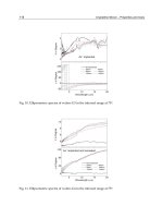
The J-V-L curve and efficiency characteristics of devices A and B are shown in Fig. 14. The
best efficiency yields of 9.44 cd/A (EQE 14.6%) and 10.62 lm/W are noticed in the device B
as shown in Fig 14(b). As seen from the results of Fig. 14(a), the driving voltage in device A
with m-MTDATA:Bebq
2
:Ir(piq)
3
[4 wt%] is 6.9 V at the brightness of 1,000 cd/m
2
. The
device B with α-NPB:Bebq
2
:Ir(piq)
3
[1 wt%] shows a driving voltage of 5.4 V at 1000 cd/m
2
.
Fig. 14. Current density (J)-Voltage(V)-Luminance (L) and Efficiency characteristics of single
layer red PHOLEDs. (a) J-V-L characteristics, (b) L vs. current and power efficiencies
characteristics. Device A(4%) and Device B(1%) fully doped.
High Efficiency Red Phosphorescent Organic Light-Emitting Diodes with Simple Structure
121
In m-MTDATA, no barrier for hole injection from the surface treated ITO (5.1 eV) to the
HOMO (5.1 eV) of the m-MTDATA exists. Further, this energy level matches with the
HOMO (5.1 eV) of the Ir(piq)
3
. While, electrons injected from the cathode move freely on
the LUMO energy of Bebq
2
. In case of the device B, the HOMO energy in the α-NPB
material at 5.4 eV as against 5.1 eV in the surface treated ITO ( HOMO difference 0.3 eV)
offers some barrier to the hole injection into the emitting layer. While electrons injected
from cathode move freely over the LUMO energy of Bebq
2
. To understand the injection
barrier situation in m-MTDATA and α-NPB, J-V of hole only devices were investigated. An ideal
Ohmic contact (Giebeler et al., 1998) at ITO and m-MTDATA interface was reported.
Whereas, the NPB hole only device had reported to have the injection limited current
behavior. When a buffer layer like PEDOT:PSS (poly(3,4-ethylenedioxythiophene)-poly(4-
stylenesurfonate) or C60 was introduced at ITO interface, the Ohmic characteristic was
observed in this device (Tse et al., 2006; Koo et al., 2008). Form these previously reported
results, a high value of driving voltage in the α-NPB mixed device B due to the high
barrier to hole injection into the emitting layer was expected. However in reality, the
device B with α-NPB hole transporting host shows a lower driving voltage implying a low
resistance to the current flow. Here, devices A and B were realized using two different
hole transporting host materials having different charge carriers transport abilities,
particularly the hole mobility. α-NPB has an ambipolar transporting ability with the hole
mobility faster than that of m-MTDATA (S. W. Liu et al., 2007). Thus, mobilities of hole
carriers in these mixed host single layer systems rather than hole injection barrier at the
ITO/mixed host interface seems to be crucial in deciding the driving voltage. In order to
elucidate the conduction and emission processes in single layer devices, we have
fabricated following several devices and investigated.
We have made devices C and D without Ir(piq)
3
dopant and results were compared with
those of devices A and B, respectively. Fig. 15 shows J-V characteristics of devices
A,B,C,D. Results on bi-layered ITO/-NPB (40 nm) / Bebq
2
: Ir(piq)
3
(10 wt%, 50 nm) /LiF
(0.5 nm) /Al(100 nm) red emitting PHOLEDs [73], reproduced here for better comparison,
show a low driving voltage value of 4.5 V to reach a luminance of 1000 cd/m
2
. As
displayed in Fig. 15, both devices C and D (undoped) show J-V characteristics similar to
Ir(piq)
3
doped devices A and B, respectively. Furthermore in our devices A and B, hole
and electron injection barriers by dopant molecules are negligible due to no barrier at ITO
and cathode interfaces, respectively. Doping in the device may affect carrier mobility due
to carrier trapping by dopant molecules. Usually, J-V characteristics of PHOLEDs are
changed significantly by adding dopant molecules when HOMO-HOMO and LUMO-
LUMO differences between host and dopant molecules are high over 0.3 eV. In device C
and D, these energy differences are within 0.3 eV. In this case, the J-V characteristic does
not change because trapped charges in dopant molecules easily overcome to host energy
level by thermal energy. Described results demonstrate that the conduction of current in a
hole and electron transporting mixed host layer is almost independent of (i) the charge
trapping at dopant molecules and (ii) hole injection barrier at the ITO/mixed host
interface. Further, all mixed single layer devices offer a high resistance to current flow
than bi-layered red device with hetero junction (see Fig. 15). The interesting and
intriguing results on J-V in mixed host single layer devices may be explained on the basis
of existing knowledge on carrier mobilities in organic materials. α-NPB exhibits an
ambipolar transporting ability with electron and hole mobility values of 9×10
-4
and 6×10
-4
cm
2
/Vs, respectively (S. W. Liu et al., 2007), while the hole mobility value in m-MTDATA
Organic Light Emitting Diode – Material, Process and Devices
122
is 3×10
-5
cm
2
/Vs. Earlier, it was shown that the charge transport behaviors in mixed thin
films of -NPB and Alq
3
are sensitive to (i) compositional fraction, and (ii) charge carriers
mobilities of neat compounds (S. W. Liu et al., 2007). The 1:1 mixed layer of -NPB and
Alq
3
appeared to give lower charge carrier mobility of 10
-2
~10
-3
order than neat films (S.
W. Liu et al., 2007). As a consequence, the fast current flow in the device B despite the
large hole injection barrier is attributed to the high hole mobility value and ambipolar
nature of -NPB. Higher driving voltage of single layer devices compared to the bilayer
device is also well understood by the decrease in carrier mobility in the mixed host
system.
Bilayered device: ITO/-NPB (40 nm) / Bebq
2
: Ir(piq)
3
(10 wt%, 50 nm) /LiF (0.5 nm)/Al(100 nm);
Device A: ITO/m-MTDATA:Bebq
2
: Ir(piq)
3
[4 wt%, 100 nm]/LiF (0.5 nm)/Al (100 nm); Device B:
ITO/α-NPB:Bebq
2
: Ir(piq)
3
[1 wt%, 100 nm]/LiF (0.5 nm)/Al (100 nm); Device C: ITO/m-
MTDATA:Bebq
2
[100 nm]/LiF (0.5 nm)/Al (100 nm); Device D: ITO/α-NPB:Bebq
2
[100 nm]/LiF (0.5
nm)/Al (100 nm)
Fig. 15. J-V characteristics of bi-layered and A~D red emitting PHOLEDs devices.
Since the charge transport behaviors in mixed hosts are sensitive to the composition and
intrinsic mobilities in neat films, the location of the recombination region may be important
to understand the device efficiency. To investigate the recombination zone position, we have
evaluated three devices with doped emissive layer located at different positions as:
1. Device A-(L) : ITO/m-MTDATA:Bebq
2
:Ir(piq)
3
[4 wt%, 30 nm]/m-MTDATA:Bebq
2
[70
nm]/LiF (0.5 nm)/Al (100 nm);
2. Device A-(C) : ITO/m-MTDATA:Bebq
2
[35 nm]/m-MTDATA:Bebq
2
:Ir(piq)
3
[4 wt%, 30
nm]/m-MTDATA:Bebq
2
[35 nm]/LiF (0.5 nm)/Al (100 nm);
3. Device A-(R) : ITO/m-MTDATA:Bebq
2
[30 nm]/m-MTDATA:Bebq
2
:Ir(piq)
3
[4 wt%, 70
nm]/LiF (0.5 nm)/Al (100 nm).
Similarly, Devices B-(L), (C) and (R) were fabricated using -NPB instead of m-MTDATA
and 1 wt% of Ir(piq)
3
. The doping region was fixed to 30 nm in all devices. The anode side
doped devices show the best current efficiency performance as displayed in Fig. 16
(Devices A-(L) and B-(L) ), indicating that the recombination zone is around the
ITO/mixed host interface. Further, the emission efficiency performance deteriorates as the
High Efficiency Red Phosphorescent Organic Light-Emitting Diodes with Simple Structure
123
doped region is moved toward the cathode side. High current efficiency in -NPB/Bebq
2
mixed host system is the consequences of the better charge balance in the recombination
zone. Figure 17 shows electroluminescence (EL) spectra dependence on the emission zone
location in doped and undoped devices. Broad and clean EL peak at 620 nm in undoped
mixed m-MTDATA/Bebq
2
host organic device C is due to exciplex emissions. While the
strong and asymmetric EL emission peak at 620 in devices A- (L) to A- (R) due to
emissions of exciplex and Ir(piq)
3
red phosphorescent dopant are noticed. In these
devices, exciplexes are formed as the energy difference between HOMO of m-MTDATA
and LUMO of Bebq
2
is about 2.3 eV. Whereas in case of fully doped (device B) and
undoped (device D) α-NPB/Bebq
2
mixed devices, clean peaks at 510 and 620 nm due to
strong emission of Bebq
2
and Ir(piq)
3
dopant are appeared, respectively. Upon moving the
doped region toward the anode side, EL spectra show both emission peaks at 510 and 620
nm due to Bebq
2
host and Ir(piq)
3
dopant, respectively, but with the reduced intensity of
510 nm emission peak of Bebq
2
. The electron charge carriers are transported over the
LUMO of Bebq
2
through the doped region and reach the anode side, resulting in the
emission due to Bebq
2
host.
Fig. 16. Luminance-current Efficiency characteristics of various single layer devices
fabricated with different locations of doped regions. Device A – Fully doped, Device B-
Fully doped.
Device A: ITO/m-MTDATA:Bebq
2
: Ir(piq)
3
[4 wt%, 100 nm]/LiF (0.5 nm)/Al (100 nm) –
Fully doped; Device C: undoped mixed m-MTDATA/Bebq
2
organic host device
Device B: ITO/α-NPB:Bebq
2
: Ir(piq)
3
[1 wt%, 100 nm]/LiF (0.5 nm)/Al (100 nm)- Fully
doped; Device D: undoped mixed α-NPB:Bebq
2
organic host device
Although holes are easily injected into the m-MTDATA/Bebq
2
organic layer (device A),
they are slowly transported due to low hole mobility in m-MTDATA which is further
reduced in the mixed host system. While transport behavior in -NPB/Bebq
2
mixed host
system is relatively better due to the high hole mobility in α-NPB. Whereas, electrons in
both doped devices A and B are transported freely over the LUMO of the Bebq
2
. These
results corroborate that the recombination zone in devices A and B are located between the
anode and the center of the emitting layer.
Organic Light Emitting Diode – Material, Process and Devices
124
Fig. 17. Electroluminescence (EL) spectra of various single layer devices fabricated with
different locations of doped regions at the brightness of 1000 cd/m
2
.
5.4 Conclusions
In conclusion, we have demonstrated high efficiency red PHOLEDs comprising only single
emitting layer. The key to the simplification is the direct injection of holes and electrons into
the mixed host materials through electrodes. The driving voltage of 5.4 V to reach the 1000
cd/m
2
and maximum current and power efficiency values of 9.44 cd/A and 10.62 lm/W,
respectively, in the -NPB/ Bebq
2
mixed single layer structure PHOLEDs with the Ir(piq)
3
dopant as low as 1 wt% are obtained. We found that carrier mobility is significantly
important parameter to simplify the device architecture. The obtained characteristics of red
PHOLEDs pave the way to simplify the device structure with reasonable reduction in the
manufacturing cost of passive and active matrix OLEDs.
6. Ideal host and guest system
6.1 Introduction
In phosphorescent devices, theoretically 100% internal quantum efficiency (IQE) is achieved
by harvesting both singlet and triplet excitons generated by electrical injection which is four
High Efficiency Red Phosphorescent Organic Light-Emitting Diodes with Simple Structure
125
times that of fluorescent organic light-emitting devices (OLEDs) (Gong et al., 2002; Tsuzuki
et al., 2003; Adachi et al., 2000). Förster and/or Dexter energy transfer processes (Tanaka
and Tokito, 2008) between host and guest molecules play an important role in confining the
triplet energy excitons in the phosphorescent guest. This determines the triplet state
emission efficiency in PHOLEDs. Förster energy transfer (Forster, 1959) is a long range
process (up to 10 nm) due to dipole-dipole coupling of donor host and acceptor guest
molecules, while Dexter energy transfer (Dexter, 1953) is a short range process (typically 1
to 3 nm) which requires overlapping of the molecular orbital of adjacent molecules
(intermolecular electron exchange).
The phosphorescence emission in the conventional host-guest phosphorescent system
occurs either with Förster transfer from the excited triplet S
1
state of the host to the excited
triplet S
1
state of the guest and Dexter transfer from the excited triplet T
1
state of the host to
the excited triplet T
1
state of the guest or direct exciton formation on the phosphorescent
guest molecules, resulting in a reasonable good efficiency. However, emission mechanism in
phosphorescent OLEDs whether due to charge trapping by guest molecules and/or energy
transfer from the host to the guest, is not clearly understood. Till date, several researchers
have reported that the charge trapping at guest molecules is the main cause for the emission
of PHOLEDs.
Amongst well-known iridium (III) and platinum (II) phosphorescent emitters, Iridium (III)
complexes have been shown to be the most efficient triplet dopants employed in highly
efficient PHOLEDs (Adachi et al., 2001b; Baldo et al., 1999). Usually, wide energy gap 4,4’-
bis(N-carbazolyl)-1,1’-biphenyl (CBP) is used as a host material for red ( 2.0 eV) or green (
2.3 – 2.4 eV) phosphorescent guests [63, 64]. Such a wide energy gap host has the advantage
of high T
1
energy of 2.6 eV (Baldo & Forrest, 2000) or 2.55 eV (Tanaka et al., 2004) and long
triplet lifetime > 1 s (Baldo & Forrest, 2000), while the optical band gap value (E
g
) is 3.1 eV
(Baldo et al., 1999).
Fig. 18(a) shows both the energy level diagram of fac-tris(2-phenyl-pyridinato)iridium(III)
(Ir(ppy)
3
) green and the tris(1-phenylisoquinoline)iridium (Ir(piq)
3
) red phosphorescent
complexes used in doping the CPB host. However, the wide band gap host and narrow
band gap (E
g
) guest system often causes an increase in driving voltage due to the difference
in HOMO and/or LUMO levels between the guest and host materials (Tsuzuki & Tokito,
2007). Thus, the guest molecules are thought to act as deep trapping centers for electrons
and holes in the emitting layer, causing an increase in the drive voltage of the PHOLED
(Gong et al., 2003). The dopant concentration in such a host-guest system is usually as high
as about 6 ~ 10 percent by weight (wt%) because injected charges move through dopant
molecules in the emitting layer. Therefore, self-quenching or triplet-triplet annihilation by
dopant molecules is an inevitable problem in host-guest systems with high doping
concentrations. Earlier, Kawamura et al. had reported that the phosphorescence
photoluminescence quantum efficiency of Ir(ppy)
3
could be decreased by ~5% with an
increasing in doping concentration from 2 to 6% (Kawamura et al., 2005). Consequently, the
selection of suitable host candidates is a critical issue in fabricating high efficiency
PHOLEDs.
In this section, the minimized charge trapped host-dopant system is investigated by using a
narrow band-gap fluorescent host material in order to address device performance and
manufacturing constraints. Here, we report an ideal host-guest system that requires only 1%
guest doping condition for good energy transfer and provides ideal quantum efficiency in
PHOLEDs. We also report that strong fluorescent host materials function very well in
Organic Light Emitting Diode – Material, Process and Devices
126
phosphorescent OLEDs due to efficient Förster energy transfers from the host singlet state to
the guest singlet and triplet mixing state which appears to be the key mechanism.
6.2 Experimental
N,N’-di(4-(N,N’-diphenyl-amino)phenyl)-N,N’-diphenylbenzidine (DNTPD) as a hole
transporting layer, CBP and bis(10-hydroxybenzo [h] quinolinato)beryllium complex
(Bebq2) as host materials, bis(2-phenylquinoline)(acetylacetonate)iridium (Ir(phq)2acac),
tris(1-phenylisoquinoline)iridium (Ir(piq)3) as red dopants, aluminum (III) bis(2-methyl-8-
quinolinato)-4-phenylphenolate (BAlq) as a hole blocking layer and Tris-(8-
hydroxyquinoline)aluminum (Alq
3
)
as
an electron transporting layer were purchased from
Gracel and Chemipro Corporation and were used. The fabricated devices are characterized as
described in the section 3. The OLED area was 2 mm
2
for all the samples studied in this work.
Fig. 18. (a) Energy level diagram of the Ir(ppy)
3
green and Ir(piq)
3
red phosphorescent
complex doped by the CPB host. (b) Energy level diagram of the Bebq
2
fluorescent host and
(Ir(phq)
2
acac) and Ir(piq)
3
red phosphorescent dopant materials.
6.3 Results & discussion
Fig. 18(b) shows an energy band diagram of the fluorescent host and orange-red
phosphorescent dopant materials used in the device fabrication. The simple bilayer
PHOLED comprises a DNTPD hole transport layer (HTL), a Bebq
2
narrow band gap
fluorescent host and an electron transport layer (ETL) plus Ir(phq)
2
acac dopant. In the
present investigation, the fabricated PHOLED was:
ITO/DNTPD (40 nm) / Bebq
2
: Ir(phq)
2
acac (50 nm, 1%)/ LiF(0.5 nm) / Al(100 nm).
Fig. 19 (a) & (b) and Table 8 (Device B) illustrate the electrical performance of the fabricated
phosphorescent device. A luminance of 1000 cd/m
2
was obtained with a driving voltage of
3.7 V, and current and power efficiency values of 20.53 cd/A and 23.14 lm/W, respectively.
High Efficiency Red Phosphorescent Organic Light-Emitting Diodes with Simple Structure
127
Furthermore, the maximum current and power efficiencies were 26.53 cd/A and 29.58
lm/W, respectively. The external quantum efficiency (EQE) value of 21% in the fabricated
PHOLED slightly exceeded the theoretical limit of about 20% derived from simple classical
optics. Moreover, this can be further improved by optimizing the output coupling. These
remarkable results brought some pleasant surprises.
Ir(phq)
2
acac concentration
(wt%)
Device A
(0.5)
Device B
(1.0)
Device C
(1.5)
Device D
(2.0)
Turn-on voltage (V)
(at 1 cd/m
2
)
2.1
2.1
2.1
2.1
Operating voltage (V)
(1000 cd/m
2
)
3.7
3.7
3.6
3.6
Efficiency (at 1000 cd/m
2
)
Current (cd/A)
Power (lm/W)
20.96
18.29
20.53
23.14
22.61
19.73
21.45
18.72
Maximum Efficiency
Current (cd/A)
Power (lm/W)
21.25
24.62
26.53
29.58
23.46
29.94
22.73
27.94
CIE (x,y) (1000 cd/m
2
)
(0.61,0.38)
(0.62,0.37)
(0.62,0.37)
(0.62,0.37)
EQE (%)(maximum)
16.6
21.0
18.9
18.6
Table 8. Key parameters from Bebq
2
:Ir(phq)
2
acac (0.5 – 2 wt%) orange-red emitting
ITO/DNTPD (40nm) / Bebq
2
: Ir(phq)
2
acac (50 nm, 0.5 to 2%)/ LiF(0.5 nm) /Al(100 nm)
PHOLED devices.
Indeed, because of the extraordinarily low doping concentration ( 1%) by contrast with
most phosphorescent devices (6 ~ 10 wt%), the enhancement of the performance of
Bebq
2
:Ir(phq)
2
acac PHOLEDs was never expected. In order to investigate the origin for the
enhanced performance, we fabricated several PHOLEDs by varying the doping
concentration from 0.5 to 2% in the host-guest system. Current and luminance as a function
of voltage are presented in Fig. 19(a), while current and power efficiencies as a function of
luminance are presented in Fig. 19(b). This data provides evidence for: (1) complete energy
transfer from the fluorescent host to phosphorescent guest, except at extremely low doping
concentrations (~0.5%); (2) no significant difference between measured I-V characteristics
for identical devices but with different dopant concentrations lying between 0.5 and 2 wt%;
Organic Light Emitting Diode – Material, Process and Devices
128
and, (3) the quenching of both luminance, and current and power efficiencies with higher
doping concentrations (~ 2 wt%). A summary of the key electrical and optical parameters
(Table 8) reveals the excellent device performance for doping concentration as low as 0.5 –
2%, in contrast with conventional PHOLEDs which require a guest concentration typically
in the range of 6 to 10 wt%. Therefore, a highly efficient simple bilayer PHOLED structure
with a Ir(phq)
2
acac guest doping concentration as low as 1% in the narrow band gap Bebq
2
fluorescent host is demonstrated here. Previously, (ppy)
2
Ir(acac):Ir(piq)
3
(0.3 – 1wt %) red
(Tsuzuki & Tokito, 2007) and CBP:Ir(phq)
2
acac (6 wt%) orange-red PHOLEDs (Kwong et al.
2002) demonstrated an EQE of 9.2% with a power efficiency of 11.0 lm/W and a power
efficiency of 17.6 cd/A with an EQE of 10.3% at 600 nit, respectively.
Fig. 19. (a) A J-V-L plot and (b) Current and power efficiencies as a function of luminance
from red PHOLEDs doped with different concentrations (0.5 – 2 %) of Ir(phq)
2
acac.
Figure 20 provides an evidence of energy transfer from the Bebq
2
fluorescent host to the
Ir(phq)
2
acac phosphorescent guest by comparing the electroluminescence (EL) spectra of
High Efficiency Red Phosphorescent Organic Light-Emitting Diodes with Simple Structure
129
PHOLEDs as a function of Ir(phq)
2
acac doping concentration from 0.5 to 2%. The strong red
light emission peak at 605 nm for all EL curves at 1000 nit is attributed to the
phosphorescence of Ir(phq)
2
acac. The Commission Internationale de l’Eclairage (CIE) color
emission coordinates are (0.61, 0.38), (0.62, 0.37), (0.62, 0.37), (0.62, 0.37) for doping
concentrations of 0.5, 1.0, 1.5, and 2.0 wt% of Ir(phq)
2
acac, respectively (as seen in Fig. 21). A
slight emission at 500 nm due to the Bebq
2
host plus a dominant doping peak at 605 nm
when the doping concentration is extremely low ( 0.5%), suggests an incomplete energy
transfer from the Bebq
2
host to the Ir(phq)
2
acac guest. Furthermore, it indicates that the
recombination of injected holes and electrons occurs at host molecule sites and then the
excited energy is rapidly transferred from the host to the guest. The presence of a clean EL
peak (no emissions at 500 nm) in other devices with doping concentrations of Ir(phq)
2
acac >
0.5% indicates a complete energy transfer from the host to the guest.
Fig. 20. EL spectra as a function of dopant concentration: Ir(phq)
2
acac of an ITO/DNTPD (40
nm) / Bebq
2
: Ir(phq)
2
acac (50 nm, 0.5 to 2%)/ LiF(0.5 nm) / Al(100 nm) PHOLEDs at 1000
cd/m
2
.
To understand the phosphorescence emission mechanism more precisely in the
Bebq
2
:Ir(phq)
2
acac host-guest system, we fabricated a series of PHOLEDs and studied. At
first, we used the well known wide band gap CBP host material instead of Bebq
2
and
fabricated the multilayer devices with a structure: NPB (40nm) / CBP:Ir(piq)
3
(30nm, 10%)
/ BAlq (5nm) / Alq
3
(20nm) / LiF (0.5nm) / Al (100nm) (Device A) and NPB (40nm) /
CBP:Ir(phq)
2
acac (30nm, 10%) / BAlq (5nm) / Alq
3
(20nm) / LiF (0.5nm) / Al (100nm)
(Device B). Table 9 displays the electrical performance of the fabricated phosphorescent
devices. At a luminance of 1000 cd/m
2
the resultant operating voltage was 7.1 V with
current and power efficiencies of 14.41 cd/A and 6.28 lm/W, respectively, and an EQE of
11.5%. Furthermore, the maximum current and power efficiency values were 14.43 cd/A
and 8.99 lm/W, respectively. Obviously, the two fold increase in driving voltage is a
consequence of the trapping of injected holes and electrons at deep Ir(phq)
2
acac molecules
in the CBP:Ir(phq)
2
acac system. Direct charge trapping on the Ir(phq)
2
acac guest molecules
seems to be the key mechanism for phosphorescence emission in this host-guest system.
Later, bilayer PHOLED device was fabricated using Ir(piq)
3
red emitting phosphorescent
doping instead of Ir(phq)
2
acac and a Bebq
2
host. The fabricated devices were: DNTPD
Organic Light Emitting Diode – Material, Process and Devices
130
(40nm) / Bebq
2
:Ir(piq)
3
(50 nm, 410 wt%) / LiF (0.5 nm) / Al (100 nm). Current density-
Voltage-Luminance and current and power efficiencies as a function of luminance plots are
shown in Fig. 22. Electrical performances of the fabricated phosphorescent devices are
illustrated in Table 10. A weak emission peak at 500 nm in the EL spectra due to the Bebq
2
host arises at a doping concentration of 4 wt% (significantly high by comparison with an
Ir(phq)
2
acac doping concentration 0.5 wt%), accompanied by a strong peak at 620 nm (CIE
coordinates x = 0.67 and y = 0.32) due to an Ir(piq)
3
doping molecule (Fig. 23). At luminance
of 1000 cd/m
2
, the corresponding operating voltage, current and power efficiencies were
3.5V, 8.41 cd/A and 7.34 lm/W, respectively. Furthermore, the maximum current and
power efficiency values were 9.38 cd/A and 11.72 lm/W, respectively. Increasing the
Ir(piq)
3
concentration to 6 wt% suppresses the Bebq
2
host emission and results in a clean EL
red emitting peak at 620 nm due to the Ir(piq)
3
doping molecules. However, the device
performance deteriorates with increasing doping concentration due to a self quenching
process as seen in Table 10.
Parameters
Device A
CBP:Ir(piq)
3
Device B
CBP:Ir(phq)
2
acac
Turn-on voltage (at 1 cd/m
2
)
3.3 V
3.1 V
Operating voltage (1000 cd/m
2
)
7.2 V
7.1 V
Efficiency (1000 cd/m
2
)
5.71 cd/A
2.49 lm/W
14.41 cd/A
6.28 lm/W
Efficiency (Maximum)
6.47 cd/A
4.45 lm/W
14.43 cd/A
8.99 lm/W
CIE (x,y) (1000 cd/m
2
)
(0.66, 0.33)
(0.61, 0.38)
Quantum efficiency (maximum)
11.2 %
11.5 %
Roll off (1000 nt vs 10000 nt)
48 %
86 %
Table 9. Electrical performance of the multilayer CBP:Ir(piq)
3
(Device A) and
CBP:Ir(phq)
2
acac (Device B) fabricated phosphorescent devices
High Efficiency Red Phosphorescent Organic Light-Emitting Diodes with Simple Structure
131
The primary mechanism for the phosphorescence emission in the Bebq
2
:Ir(piq)
3
host-guest
system (Fig. 18 (b)) appears to be due to the energetically favorable electron transport and
hole trapping at deep trapping centers in Ir(piq)
3
molecules. Thus, an appropriate selection
of the host and phosphorescent dopant materials plays a significant role in determining the
emission mechanism on phosphorescent devices. These results on phosphorescent emission
in Bebq
2
:Ir(phq)
2
acac host-guest systems are very interesting and intriguing. The mechanism
of phosphorescence emission is not believed to be due to the direct charge trapping in
Ir(phq)
2
acac phosphorescent guest molecules. Attempts have been made here to explain
these results on the basis of the existing knowledge of Förster and Dexter energy transfer
processes in host-guest systems.
Fig. 21. Commission Internationale de l’Eclairage (CIE) color emission coordinates of red
PHOLEDs described in Fig. 20.
Organic Light Emitting Diode – Material, Process and Devices
132
The Bebq
2
host material produces a strong fluorescence emission but no phosphorescence
emission signature even at 77 K. The efficient use of Bebq
2
host in the described
phosphorescent devices is an extraordinary phenomenon since strong fluorescent host
materials are believed to provide poor phosphorescent performance. Therefore, we suspect
efficient Förster energy transfer between the host singlet and the metal-to-ligand charge-
transfer (MLCT) state of the iridium (III) metal complex. Earlier, Förster energy transfer in
phosphorescent OLEDs was postulated by Gong et al. and Ramos-Ortiz. et al. in solid
photoluminescence studies (Gong et al., 2003; Ramos-Ortiz et al., 2002). To investigate
Förster energy transfer from the Bebq
2
host to the Ir(phq)
2
acac, time resolved spectroscopy
and a Stern-Volmer plot in THF solution measurements techniques were employed. The
Fig. 22. Current density-Voltage-Luminance and current and power efficiencies as a function
of luminance plots of DNTPD (40nm) / Bebq
2
:Ir(piq)
3
(50 nm, 410 wt%) / LiF (0.5 nm) / Al
(100 nm) red PHOLEDs
High Efficiency Red Phosphorescent Organic Light-Emitting Diodes with Simple Structure
133
singlet fluorescent lifetime of Bebq
2
is 5.0 ns. From the slope of the linear Stern-Volmer plot
(Fig. 24), the calculated energy transfer rate is k
q
= 8×10
12
sec
-1
M
-1
, indicating that the energy
transfer from the excited singlet state of the host to the dopant triplet occurs quantitatively
and ideally. Furthermore, the strong spin orbital coupling induced by the transition metal
ion indicates that a narrow energy gap exists between the
1
MLCT and
3
MLCT states (
0.3eV) and opens a pathway for efficient energy transfer from the singlet to the emitting
triplet states. Therefore, two channels for Förster energy transfer from the host singlet to the
1
MLCT and
3
MLCT states of the iridium complex are available as shown in Fig. 25.
Overlapping of the host emission and dopant absorption spectra substantiates the
hypothesis of efficient Förster energy transfer from the host singlet to the guest emitting
triplet states via two channels (Fig. 26). Furthermore, the strong fluorescent quantum
efficiency of 0.39 in the host (Bebq
2
) in solution, obtained using a relative quantum yield
measurement, favors Förster energy transfer.
Parameters
Device A
(10%)
Device B
(8%)
Device C
(6%)
Device D
(4%)
Turn-on
voltage
(at 1 cd/m
2
)
2.1 V 2.1 V 2.1 V 2.1 V
Operating
voltage
(1000 cd/m
2
)
3.5 V 3.5 V 3.5 V 3.5 V
Efficiency
(1000 cd/m
2
)
6.78 cd/A
5.92 lm/W
7.18 cd/A
6.26 lm/W
7.65 cd/A
6.68 lm/W
8.41 cd/A
7.34 lm/W
Efficiency
(Maximum)
7.38 cd/A
8.10 lm/W
7.82 cd/A
10.40 lm/W
8.37 cd/A
10.67 lm/W
9.38 cd/A
11.72 lm/W
CIE (x,y)
(1000 cd/m
2
)
(0.67,0.32) (0.67,0.32) (0.67,0.32)
(0.67,0.32)
Quantum
efficiency
(maximum)
11.4 % 13.0 % 14.4 % 16.3 %
Roll off
(1000 nt vs
10000 nt)
48 % 48 % 50 %
47 %
Table 10. Electrical performances of the fabricated DNTPD (40nm) / Bebq
2
:Ir(piq)
3
(50 nm,
410 wt%) / LiF (0.5 nm) / Al (100 nm) red phosphorescent devices
Organic Light Emitting Diode – Material, Process and Devices
134
Fig. 23. EL spectra of DNTPD (40nm) / Bebq
2
:Ir(piq)
3
(50 nm, 4 and 6 wt%) / LiF (0.5 nm) /
Al (100 nm) PHOLEDs at 8000 cd/m
2
.
Fig. 24. Stern-Volmer plot showing the effect of Bebq
2
fluorescence quenching by
(Ir(phq)
2
acac) dopant.
High Efficiency Red Phosphorescent Organic Light-Emitting Diodes with Simple Structure
135
Fig. 25. Förster and Dexter energy transfer mechanism in the Bebq
2
:Ir(phq)
2
acac system.
Fig. 26. Spectral overlapping of the photoluminescence spectrum from Bebq
2
and the
absorption spectrum from Ir(phq)
2
acac.
The Förster radius (R
0
), critical distance for the concentration quenching, was estimated as
1.3 nm (similar to a previously reported value) using the following equation:
2
64
0
54
0
9000(ln10)
() ()
128
PL
DA
A
k
RFd
Nn
where k
2
= orientation factor,
PL
= photoluminescence quantum efficiency, N
A
=
Avogadro’s number, n = refractive index,
0
() ()
DA
F
= spectral overlap integral between
donor photoluminescence (F
D
()
), and
A
()
= acceptor absorption, and = wavelength.
The triplet exciton energy transfer from the Bebq
2
host to
3
MLCT is governed by Dexter
energy transfer. The rate constant of Dexter energy transfer (Kawamura et al., 2006) is
k
ET
= K J exp (-2R
DA
/L)
Organic Light Emitting Diode – Material, Process and Devices
136
where K is related to the specific orbital interaction, J is a spectral overlap integral, and R
DA
is donor-acceptor separation relative to their van der Waals radii, L. The ideal Dexter radius
is the distance between the host and dopant molecule diameter considering overlapping
molecular orbitals in adjacent molecules (Turro, 1991a).
Using the equation: R = [(molecular density in film) × mol% of the dopant in a film]
-1/3
as
reported by Kawamura et al. (Kawamura et al., 2006) yields an average distance of about
58.5
Å and 44.9Å between Ir(phq)
2
acac molecules for doping concentrations of 0.5%, 1.0%,
respectively (Fig.27). By considering the host (13.6
Å) and dopant (13.7Å) diameters
calculated using a molecular modeling program (DMOL3) (Delley, 2000) and van der Waals
interaction distance (usually very small within 2
Å) for the ideal Dexter energy transfer
condition, the estimated distance between the host and guest molecules is about 15.6
Å (i.e.
the half diameters of the host and dopant molecules are, 13.7/2
Å plus 13.6Å/2, including a
2
Å van der Waals interaction distance). In solid state films, the minimum doping
concentration is desirable to prevent triplet quenching processes.
Considering that two host molecules are located between two dopant molecules, an ideal
Dexter condition (Fig. 27(b)), all host molecules are adjacent to a dopant molecule and
dopant molecules are well separated in the host matrix. In such a host and guest molecule
arrangement, the separation between two dopant molecules appears to be about 46.9
Å.
However, when the doping concentration is 0.5%, the estimated separation between
Ir(phq)
2
acac molecules is 58.5Å, suggesting that more than two host molecules are located
between two dopant molecules (Fig. 27(b). If the doping concentration is increased to 1%,
the separation between dopant molecules is less than 46.9
Å, which results in an efficient
energy transfer from the Bebq
2
host to the emitting triplet state of Ir(phq)
2
acac via Dexter
processes. The triplets generated due to the Bebq
2
host molecules diffuse to an average
distance of only 15.6
Å, with a doping concentration of 1 wt%, until they are harvested by
Ir(phq)
2
acac (Fig. 27(b). If the doping concentration is increased to greater than 1%, the
device performance deteriorates due to quenching processes of triplet excitons caused by
two closely separated dopant molecules.
The influence of the Förster quenching process in the described system is not serious at all
doping concentrations (Fig. 27(a). The singlet exciton energies generated by charge injection
in host molecules can be transferred to triplet states of dopant molecules by the efficient
Förster energy transfer. In our system, the rate constant of Förster energy transfer is much
faster than that of the intersystem crossing of host singlet states. Typical intersystem
crossing rate constants fall within the range ~10
6
-10
8
sec
-1
(Turro, 1991b). Thus, strong
fluorescent materials, such as Bebq
2
, are excellent as host materials in PHOLEDs.
6.4 Conclusions
In conclusion, we have demonstrated here an ideal host-guest energy transfer and quantum
efficiency conditions with a dopant concentration of approximately 1% in phosphorescent
OLEDs. We also report that strong fluorescent host materials function very well in
phosphorescent OLEDs. The operating mechanism for the phosphorescence emission is
twofold: Firstly, an efficient Förster energy transfer process from the host singlet exciton to
the
1
MLCT and
3
MLCT states of the guest. And, secondly, a Dexter energy transfer process
from the host triplet exciton to the
3
MLCT state of the guest. The extremely low doping
concept for highly efficient PHOLEDs has potential uses in future display and lighting
applications.
High Efficiency Red Phosphorescent Organic Light-Emitting Diodes with Simple Structure
137
Fig. 27. (a) Förster and Dexter energy transfer conditions as a function of doping
concentration and distance between two dopants. (b) The molecular diameters of the host
and dopant and the dopant-dopant distance for an ideal Dexter energy transfer.
7. Conclusions
Simple structure red PHOLED, using narrow band gap fluorescent host materials have
been demonstrated
, having a:
(1) Simple structure, (2) Low driving voltage, (3) High efficiency (lm/W), (4) No charge trapping at
phosphorescent guest molecules, (5) Low doping concentration, and (6) Low manufacturing cost.
These results are summarized in Table 11. Various triplet quantum well devices from a
single to five quantum wells are realized using a wide band-gap hole and an electron
transporting layers, Bebq
2
narrow band-gap host and Ir(piq)
3
red dopant materials, and
Organic Light Emitting Diode – Material, Process and Devices
138
Bepp
2
charge control layers (CCL). Triplet energies in fabricated MQW devices are confined
at the emitting layers. The maximum external quantum efficiency of 14.8 % with a two
quantum well device structure is obtained, which is the highest value among the reported
Ir(piq)
3
dopant red phosphorescent OLEDs. The described MQW device concept can be very
useful to future OLED display and lighting applications.
Parameters
1
MQW p-
i-n device
n=2
2
Bilayer
device
3
Single
Layer
4% Doping
4
Single
Layer
1% Doping
5
Ideal host-
Guest
Device
(1%)
Turn on voltage
(@ 1cd/m
2
)
2.5 V
2.3 V
2.4 V
2.1
Operating voltage
(@ 1000 cd/m
2
)
4.2 V
4.5V
6.9 V
5.4 V
3.7
Current (cd/A) &
Power (lm/W)
efficiencies @ 1000
cd/m
2
9.66,
6.90
7.44,
3.43
9.02,
5.25
20.53
23.14
Maximum
Current (cd/A) &
Power (lm/W)
Efficiencies
12.4
8.04,
10.96
9.44,
10.62
26.53,
29.58
CIE (x, y)
(@ 1000 cd/m
2
)
(0.66,
0.33)
(0.67, 0.33)
(0.67, 0.32)
(0.66, 0.33)
(0.62, 0.37)
EQE (%)
(maximum)
14.8
21.0
1
ITO/TCTA:WO
3
(30%,40nm)/TCTA(12nm)/Bebq
2
:Ir(2%,10nm)/Bepp
2
(CCL,5nm)(n=2) /Bepp
2
(7 nm)/Bepp
2
:Cs
2
CO
3
(10%, 20 nm)/ Al(100 nm)
2
ITO/α-NPB (40 nm) / Bebq
2
: Ir(piq)
3
(10 wt%, 50 nm)/ LiF(0.5 nm) / Al(100 nm
3
ITO/m-MTDATA:Bebq
2
: Ir(piq)
3
(4 wt%, 100 nm)/LiF (0.5 nm)/Al (100 nm)
4
ITO/α-NPB:Bebq
2
: Ir(piq)
3
(1 wt%, 100 nm)/LiF (0.5 nm)/Al (100 nm).
5
ITO/DNTPD (40nm) / Bebq
2
: Ir(phq)
2
acac (50 nm, 1%)/ LiF(0.5 nm) /Al(100 nm)
Table 11. Summary of performances of red PHOLEDs in this study
Bi-layered simple structure red PHOLED demonstrates high current and power efficiency
values of 9.66 cd/A and 6.90 lm/W, respectively. The operating voltage of bi-layered
PHOLEDs at a luminance of 1000 cd/m
2
was 4.5 V. A simple bilayerd red emitting device
with Bebq
2
host could be a promising way to achieve efficient, economical, and ease
manufacturing process, important for display and lighting production.
High Efficiency Red Phosphorescent Organic Light-Emitting Diodes with Simple Structure
139
We have also demonstrated high efficiency red PHOLEDs comprising only single emitting
layer. The driving voltage of 5.4 V to reach the 1000 cd/m
2
and maximum current and
power efficiency values of 9.44 cd/A and 10.62 lm/W, respectively, in the -NPB/ Bebq
2
mixed single layer structure PHOLEDs with the Ir(piq)
3
dopant as low as 1 wt% are
obtained. The obtained results could be useful to simplify the device structure with a
reasonable reduction in the manufacturing cost of passive and active matrix OLEDs.
An ideal host-guest system displays efficient energy transfer and quantum efficiency
conditions with a dopant concentration of approximately 1% in phosphorescent OLEDs. A
luminance of 1000 cd/m
2
was obtained with a driving voltage of 3.7 V, and current and
power efficiencies of 20.53 cd/A and 23.14 lm/W (maximum current efficiency: 26.53 cd/A
and maximum power efficiency: 29.58 lm/W), respectively. The external quantum efficiency
(EQE) value of 21% in the fabricated PHOLED, slightly exceeded the theoretical limit of
about 20% derived from simple classical optics, is recorded.
In summary, narrow band gap fluorescent host materials with the extremely low doping
concept for highly efficient PHOLEDs has potential uses in future display and lighting
applications.
8. Acknowledgement
Authors are thankful to Professor Yup Kim, Physics Department (Kyung Hee University,
Seoul) for his encouragement during the span of this work.
9. References
Al Attar, H.A., Monkman, A.P., Tavasli, M., Bettington, S. & Bryce, M.R. (2005). White
polymeric light-emitting diode based on a fluorine polymer⁄Ir complex blend
system, Appl. Phys. Lett. 86: 121101-1 – 121101-3.
Adachi, C., Baldo, M.A., Forrest, S.R. & Thompson, M.E. (2000). High-efficiency organic
electrophosphorescent devices with tris(2-phenylpyridine)iridium doped into
electron-transporting materials, App. Phys. Lett. 77: 904-906.
Adachi, C., Baldo, M.A., Forrest, S.R., Lamansky, S., Thompson, M.E. & Kwong, R.C.
(2001a). High-efficiency red electrophosphorescence devices, Appl. Phys. Lett. 78:
1622-1624.
Adachi, C., Baldo, M. A., Thompson, M. E. & Forrest, S. R. (2001b). Nearly 100% internal
phosphorescence efficiency in an organic light-emitting device, J. Appl. Phys. 90:
5048-5051.
Adamovich, V.I., Cordero, S.R., Djurovich, P.I., Tamayo, A., Thompson, M.E., D’Andrade, B.
W. & Forrest, S.R. (2003). New charge-carrier blocking materials for high efficiency
OLEDs, Org. Electron. 4 (2-3): 77-87.
Baldo, M.A., O’Brien, D.F., You, Y., Shoustikov, A., Sibley, S., Thompson, M.E. & Forrest,
S.R. (1998). Highly efficient phosphorescent emission from organic
electroluminescent devices, Nature (London) 395: 151-154.
Baldo, M. A., Lamansky, S., Burrows, P. E., Thompson, M. E. & Forrest, S. R. (1999). Very
high-efficiency green organic light-emitting devices based on
electrophosphorescence, Appl. Phys. Lett. 75: 4-6.
Organic Light Emitting Diode – Material, Process and Devices
140
Baldo, M. A. & Forrest, S. R. (2000). Transient analysis of organic electrophosphorescence: I
Transient analysis of triplet energy transfer, Phy. Rev. B 62, 10958-10966.
Bulovic, V., Khalfin, V. B., Gu, G. & Burrows, P. E. (1998). Weak microcavity effects in
organic light-emitting devices, Phys. Rev. B 58: 3730-3740.
Che, G., Su, Z., Li, W., Chu, B., Li, M., Hu, Z. & Zhang, Z. (2006). Highly efficient and color-
tuning electrophosphorescent devices based on Cu
I
complex, Appl. Phys. Lett. 89:
103511-1 – 103511-3.
Chen, P., Xue, Q., Xie, W., Duan, Y., Xie, G., Hou, J., Liu, S., Zhang, L. & Li, B. (2008). Color-
stable and efficient stacked white organic light-emitting devices comprising blue
fluorescent and orange phosphorescent emissive units, Appl. Phys. Lett. 93: 153508-1
– 153508-3.
Chin, B. D., Suh, M. C., Kim, M. H., Lee, S. T., Kim, H. D. & Chung, H. K. (2005). Carrier
trapping and efficient recombination of electrophosphorescent device with
stepwise doping profile, Appl. Phys. Lett. 86: 133505-1 – 133505-3.
Coushi, K., Kwon, R., Brown, J. J., Sasabe, H. & Adachi, C. (2004). Triplet exciton
confinement and unconfinement by adjacent hole-transport layers, J. Appl. Phys. 95:
7798-7802.
D’Andrade, B.W., Holmes, R.J. & Forrest, S.R. (2004).
Efficient organic
electrophosphorescent white-light-emitting device with a triple doped emissive
layer, Adv. Mater. 16: 624-628.
D’Andrade, B. W. & Forrest, S. R. (2004). White organic light-emitting devices for solid- state
lighting, Adv. Mater. (Weinheim, Ger.) 16: 1585-1595.
Delley, B. (2000). From molecules to solids with the DMoL3 approach, J. Chem. Phys. 113:
7756-7764.
Deng, Z. B., Ding, X. M., Lee, S.T. & Gambling, W.A. (1999). Enhanced brightness and
efficiency in organic electroluminescent devices using SiO
2
buffer layers, Appl. Phys.
Lett. 74: 2227-2279.
Destruel, P., Jolinat, P., Clergereaux, R. & Farenc, J. (1999). Pressure dependence of electrical
and optical characteristics of Alq
3
based organic electroluminescent diodes, J. Appl.
Phys. 85: 397-400.
Dexter, D.L. (1953). A Theory of Sensitized Luminescence in Solids, J. Chem. Phys. 21: 836-
850.
Duan, J P., Sun, P P. & Cheng, C H. (2003). New iridium complexes as highly efficient
orange-red emitters in organic light-emitting diodes, Adv. Mater. 15, 224-228.
Endo, J., Matsumoto, T. & Kido, J. (2002). Organic Electroluminescent Devices Having Metal
Complexes as Cathode Interface Layer, Jpn. J. Appl. Phys. 41: L800-L803.
Forster, T. (1959). Transfer mechanisms of electronic excitation, Discuss. Faraday Soc. 27: 7-17.
Friend, R. H., Gymer, R. W., Holmes, A. B., Burroughes, J. H., Marks, R. N., Taliani, C.,
Bradley, D. D. C., Dos Santos, D. A., Bredas, J. L., Logdlund, M. & Salaneck, W. R.
(1999). Electroluminescence in conjugated polymers, Nature (London) 397, 121-128.
Fukase, A. & Kido, J. (2002). High efficiency organic electroluminescent devices using
Iridium complex emitter and arylamine-containing polymer buffer layer, Polym.
Adv. Technol. 13: 601-604.