Advanced Microwave and Millimeter Wave technologies devices circuits and systems Part 2 pot
Bạn đang xem bản rút gọn của tài liệu. Xem và tải ngay bản đầy đủ của tài liệu tại đây (2.09 MB, 40 trang )
AdvancedMicrowaveandMillimeterWave
Technologies:SemiconductorDevices,CircuitsandSystems32
6. Acknowledgement
The author would like to thanks Vedran Kordic for invitation me as an editor of the present
book. The preparation of this chapter would not have been possible without the support of
our father and mother.
7. References
1. Anishchenko, Y. V. (1997). Radiation Initiated by a Surface Wave Propagating along a
Long Plasma Column with a Varying Impedance. Plasma Physics Reports, Vol. 23
No. 12, pp. 1001-1006.
2. Askar’yan G. A. (1982). Letters to journal of technical physics (JTF), Vol. 8, pp. 1131.
3. Dwyer, T.J., Greig, J.R., Murphy, D.P., Perin, J.M., Pechacek, R.E., and Raleigh, M. (1984).
On the Feasibility of Using an Atmospheric Discharge Plasma as an RF Antenna.
IEEE Transactions on Antennas and Propagation, Vol. AP-32. No.2, pp.78-83.
4. Alexeff, I., Kang, W. L., Rader, M., Douglass, C, Kintner, D., Ogot, R., and Norris, E.
(2000). A Plasma Stealth Antenna for the U. S. Navy-Recent Results. Plasma Sources
and Applications of Plasmas II, November 18.
5. Larry L. Altgilbers et al. (1998). Plasma antennas: theoretical and experimental
conciderations. Plasmadynamics and Lasers Conference, 29th, Albuquerque, NM, June
15-18. AIAA-1998-2567.
6. Zhang T. X., Wu S. T., Altgilbers L. L., Tracy P., and Brown M. Radiation Mechanisms of
Pulsed Plasma Dielectric Antennas, 2002, AIAA-2002-2104.
7. Novikov V.E., Puzanov A.O., Sin’kov V.V., Soshenko V.A. (2003). Plasma antenna for
magneto cumulative generator. Int. Conf. On antenna theory and techniques, Sept. 9-
12. Ukraine, pp. 692-695.
8. Shkilyov A.L., Khristenko V.M., Somov V.A., Tkach. Yu.V. (2003). Experimental
Investigation of Explosive Plasma Antennas. Electromagnetic phenomenon’s, Vol. 3, N
4(12), pp.521-528.
9. Schoeneberg N.J. (2003). Generation of transient antennas using cylindrical shaped
charges, A THESIS IN ELECTRICAL ENGINEERING, Submitted to die Graduate
Faculty of Texas Tech University in Partial Fulfillment of the Requirements for the
Degree of MASTER OF SCIENCE IN ELECTRICAL ENGINEERING.
10. Minin I., Minin O. (2002). The possibility of impulse plasma antenna creation, Proceeding
of the 6th Russian-Korean Int. Symp. On Science and Technology, June 24-30,
Novosibirsk, Russia. v.2, pp. 289 – 292.
11. Minin I.V., Minin O.V. (1998). Diffractional quasioptics. 180 p. Moskow: ImformTei.
12. Kennedy, D. R. (1983). History of the Shaped Charge Effect, the First 100 Years, 75p. U. S.
Department of Commerce, AD-A220 095.
13. Minin I.V. and Minin O.V. (2003). World’s history of shaped charge. Proceeding of the
Russian conference “Science, Industry and defense”, Novosibirsk, April 23-25, pp.
51-53.
14. Walters, W.P. and Zukas J.A. (1989). Fundamentals of Shaped Charges. 130 p. CMCPress.
Baltimore, MD.
15. Wolsh J., Shreffler, Willing F. (1954). The limiting conditions for jet formation at high speed.
Moskoy.: Mechanics, 1(23), (in Russian).
16. Godunov S., Deribas A., Mali V. (1975). About the influences of viscous of metall to the jet
formation process. Fisika gorenia i vzriva (in Russian), Vol. 11, № 1.
17. Pei Chi Chon, J.Carleone, R.Karpp. (1976). Criteria for jet formation from impinging shell and
plates. J. Appl. Phys., Vol. 47.
18. Birkhoff G., McDougall D., Pugh E., Taylor G. (1948). Explosives with lined cavities. J. Of
Appl. Phys. Vol. 19, pp. 563-582.
19. Lavrent’ev M. (1957). The shaped charge and principles of it operations. Uspehi matem. Nauk
(in Russian). Vol. 12, № 4, pp.41-56.
20. Minin I.V., Minin O.V. (2003). New criterion of cumulative jet formation. 7th Korea-Russia
International Symposium on Science and Technology "KORUS 2003",June 29-July 2,
2003. University of Ulsan, Ulsan, Korea, vol.3, Pages: 93 – 94.
21. V.F.Minin, I.V.Minin, O.V.Minin. Criterium of jet formation for the axisymmetrical
shaped charge//Izvestia Vuzov, Povoljskii region, 2006, № 6 (27), pp. 380-389 (in
Russian).
22. Neuber, A.; Schoeneberg, N.; Dickens, J.; Kristiansen, M. (2002). Feasibility study of an
explosively formed transient antenna. Power Modulator Symposium, 2002 and 2002
High-Voltage Workshop. Conference Record of the Twenty-Fifth International
Volume , Issue , 30 June-3 July 2002, pp. 374 – 377.
23. Minin O.V. and Minin I.V. (2000). The influence of the grain size of microstructure of the
surface layer material of a hypersonic body on the properties of air plasma The 10
th
Electromagnetic Launch Technology Symposium, Institute for Advanced
Technology, San Francisco, California, USA, April 25-28, 2000. The book of
abstracts, pp. 160. See also: Minin O.V. and Minin I.V. (2000). The influence of the
grain size of microstructure of the surface layer material of a hypersonic body on the
properties of air plasma. // Computer optics, N20, pp.93-96.
24. Minin I.V., Minin O.V. (2003). Diffraction optics of millimeter waves. – IOP Publisher,
Boston-London.
25. Patent of the USA № 4100783. Minin V.F. et al. Installation for explosion machining of
articles., Jul.18, 1978.
26. Walters. W.P. An Overview of the Shaped Charge Concept
/>Concept
27. Dante, J. G. and Golaski, S. K. (1985). Micrograin and Amorphous Shaped Charge Liners.
Proceedings of ADPA Bomb and Warhead Section, White Oak, MD, May 1985.
28. Manuel G. Vigil. (2003). Design of Largest Shaped Charge: Generation of Very Large Diameter,
Deep Holes in Rock and Concrete Structures. SANDIA REPORT SAND2003-1160,
Unlimited Release, Printed April 2003.
29. Minin I.V., Minin O.V. (2002). Physical aspects of shaped charge and fragmentational
warheads. 84 p. Novosibirsk, NSTU.
30. Minin I.V., Minin O.V. (1999). Some new principles of cumulative jet formation. Collection of
works NVI (in Russian), Vol. 7, pp. 19-26. Patent SU № 1508938 (1987). Minin V.F.,
Minin I.V., Minin O.V. and et. Devise for plasma jet forming.
31. Minin I.V., Minin O.V. (1992). Analytical and computation experiments on forced plasma
jet formation. Proc. of the 2
nd
Int. Symp. on Intense Dynamic Loading and Its Effects.
Chengdu, China, June 9-12, 1992, pp. 588-591.
Explosivepulsedplasmaantennasforinformationprotection 33
6. Acknowledgement
The author would like to thanks Vedran Kordic for invitation me as an editor of the present
book. The preparation of this chapter would not have been possible without the support of
our father and mother.
7. References
1. Anishchenko, Y. V. (1997). Radiation Initiated by a Surface Wave Propagating along a
Long Plasma Column with a Varying Impedance. Plasma Physics Reports, Vol. 23
No. 12, pp. 1001-1006.
2. Askar’yan G. A. (1982). Letters to journal of technical physics (JTF), Vol. 8, pp. 1131.
3. Dwyer, T.J., Greig, J.R., Murphy, D.P., Perin, J.M., Pechacek, R.E., and Raleigh, M. (1984).
On the Feasibility of Using an Atmospheric Discharge Plasma as an RF Antenna.
IEEE Transactions on Antennas and Propagation, Vol. AP-32. No.2, pp.78-83.
4. Alexeff, I., Kang, W. L., Rader, M., Douglass, C, Kintner, D., Ogot, R., and Norris, E.
(2000). A Plasma Stealth Antenna for the U. S. Navy-Recent Results. Plasma Sources
and Applications of Plasmas II, November 18.
5. Larry L. Altgilbers et al. (1998). Plasma antennas: theoretical and experimental
conciderations. Plasmadynamics and Lasers Conference, 29th, Albuquerque, NM, June
15-18. AIAA-1998-2567.
6. Zhang T. X., Wu S. T., Altgilbers L. L., Tracy P., and Brown M. Radiation Mechanisms of
Pulsed Plasma Dielectric Antennas, 2002, AIAA-2002-2104.
7. Novikov V.E., Puzanov A.O., Sin’kov V.V., Soshenko V.A. (2003). Plasma antenna for
magneto cumulative generator. Int. Conf. On antenna theory and techniques, Sept. 9-
12. Ukraine, pp. 692-695.
8. Shkilyov A.L., Khristenko V.M., Somov V.A., Tkach. Yu.V. (2003). Experimental
Investigation of Explosive Plasma Antennas. Electromagnetic phenomenon’s, Vol. 3, N
4(12), pp.521-528.
9. Schoeneberg N.J. (2003). Generation of transient antennas using cylindrical shaped
charges, A THESIS IN ELECTRICAL ENGINEERING, Submitted to die Graduate
Faculty of Texas Tech University in Partial Fulfillment of the Requirements for the
Degree of MASTER OF SCIENCE IN ELECTRICAL ENGINEERING.
10. Minin I., Minin O. (2002). The possibility of impulse plasma antenna creation, Proceeding
of the 6th Russian-Korean Int. Symp. On Science and Technology, June 24-30,
Novosibirsk, Russia. v.2, pp. 289 – 292.
11. Minin I.V., Minin O.V. (1998). Diffractional quasioptics. 180 p. Moskow: ImformTei.
12. Kennedy, D. R. (1983). History of the Shaped Charge Effect, the First 100 Years, 75p. U. S.
Department of Commerce, AD-A220 095.
13. Minin I.V. and Minin O.V. (2003). World’s history of shaped charge. Proceeding of the
Russian conference “Science, Industry and defense”, Novosibirsk, April 23-25, pp.
51-53.
14. Walters, W.P. and Zukas J.A. (1989). Fundamentals of Shaped Charges. 130 p. CMCPress.
Baltimore, MD.
15. Wolsh J., Shreffler, Willing F. (1954). The limiting conditions for jet formation at high speed.
Moskoy.: Mechanics, 1(23), (in Russian).
16. Godunov S., Deribas A., Mali V. (1975). About the influences of viscous of metall to the jet
formation process. Fisika gorenia i vzriva (in Russian), Vol. 11, № 1.
17. Pei Chi Chon, J.Carleone, R.Karpp. (1976). Criteria for jet formation from impinging shell and
plates. J. Appl. Phys., Vol. 47.
18. Birkhoff G., McDougall D., Pugh E., Taylor G. (1948). Explosives with lined cavities. J. Of
Appl. Phys. Vol. 19, pp. 563-582.
19. Lavrent’ev M. (1957). The shaped charge and principles of it operations. Uspehi matem. Nauk
(in Russian). Vol. 12, № 4, pp.41-56.
20. Minin I.V., Minin O.V. (2003). New criterion of cumulative jet formation. 7th Korea-Russia
International Symposium on Science and Technology "KORUS 2003",June 29-July 2,
2003. University of Ulsan, Ulsan, Korea, vol.3, Pages: 93 – 94.
21. V.F.Minin, I.V.Minin, O.V.Minin. Criterium of jet formation for the axisymmetrical
shaped charge//Izvestia Vuzov, Povoljskii region, 2006, № 6 (27), pp. 380-389 (in
Russian).
22. Neuber, A.; Schoeneberg, N.; Dickens, J.; Kristiansen, M. (2002). Feasibility study of an
explosively formed transient antenna. Power Modulator Symposium, 2002 and 2002
High-Voltage Workshop. Conference Record of the Twenty-Fifth International
Volume , Issue , 30 June-3 July 2002, pp. 374 – 377.
23. Minin O.V. and Minin I.V. (2000). The influence of the grain size of microstructure of the
surface layer material of a hypersonic body on the properties of air plasma The 10
th
Electromagnetic Launch Technology Symposium, Institute for Advanced
Technology, San Francisco, California, USA, April 25-28, 2000. The book of
abstracts, pp. 160. See also: Minin O.V. and Minin I.V. (2000). The influence of the
grain size of microstructure of the surface layer material of a hypersonic body on the
properties of air plasma. // Computer optics, N20, pp.93-96.
24. Minin I.V., Minin O.V. (2003). Diffraction optics of millimeter waves. – IOP Publisher,
Boston-London.
25. Patent of the USA № 4100783. Minin V.F. et al. Installation for explosion machining of
articles., Jul.18, 1978.
26. Walters. W.P. An Overview of the Shaped Charge Concept
/>Concept
27. Dante, J. G. and Golaski, S. K. (1985). Micrograin and Amorphous Shaped Charge Liners.
Proceedings of ADPA Bomb and Warhead Section, White Oak, MD, May 1985.
28. Manuel G. Vigil. (2003). Design of Largest Shaped Charge: Generation of Very Large Diameter,
Deep Holes in Rock and Concrete Structures. SANDIA REPORT SAND2003-1160,
Unlimited Release, Printed April 2003.
29. Minin I.V., Minin O.V. (2002). Physical aspects of shaped charge and fragmentational
warheads. 84 p. Novosibirsk, NSTU.
30. Minin I.V., Minin O.V. (1999). Some new principles of cumulative jet formation. Collection of
works NVI (in Russian), Vol. 7, pp. 19-26. Patent SU № 1508938 (1987). Minin V.F.,
Minin I.V., Minin O.V. and et. Devise for plasma jet forming.
31. Minin I.V., Minin O.V. (1992). Analytical and computation experiments on forced plasma
jet formation. Proc. of the 2
nd
Int. Symp. on Intense Dynamic Loading and Its Effects.
Chengdu, China, June 9-12, 1992, pp. 588-591.
AdvancedMicrowaveandMillimeterWave
Technologies:SemiconductorDevices,CircuitsandSystems34
32. Minin I.V., Minin O.V. (2005). Cumulative plasna jet formation for acceleration of
macroparticles, 9th Korea-Russia International Symposium on Science and Technology /
KORUS 2005, June 26-July 2, 2005, NSTU, Russia.
33. Minin I.V., Minin O.V. (2006). Experimental research on reactive type plasma antenna for
secure WiFi networks, 8th Int. Conf. On actual problems on electronics instrument
engineering, Proceeding, APIEE-2006, v.2, Novosibirks, Sep.26-28, 2006.
34. Prof. Dr. V.F.Minin
35. Minin F.V., Minin I.V., Minin O.V. (1992) Technology of calculation experiments //
Mathematical modeling, v.4, N 12, pp. 78-86 (in Russian).
36. Minin F.V., Minin I.V., Minin O.V. (1992) The calculation experiment technology,
Proceedings of the 2
nd
Int. Symp. on Intense Dynamics loading and its effects, Chengdu,
China, July 9-12, pp.581-587.
Exploitingthesemiconductor-metalphasetransitionofVO2materials:anovel
directiontowardstuneabledevicesandsystemsforRFmicrowaveapplications 35
Exploitingthesemiconductor-metalphasetransitionofVO2materials:a
noveldirectiontowardstuneabledevicesandsystemsforRFmicrowave
applications
Crunteanu Aurelian, Givernaud Julien, Blondy Pierre, Orlianges Jean-Christophe,
ChampeauxCorinneandCatherinotAlain
x
Exploiting the semiconductor-metal
phase transition of VO2 materials:
a novel direction towards tuneable
devices and systems for
RF-microwave applications
Crunteanu Aurelian
1
, Givernaud Julien
1
, Blondy Pierre
1
,
Orlianges Jean-Christophe
2
, Champeaux Corinne
2
and Catherinot Alain
2
1
XLIM, CNRS/ Université de Limoges
2
SPCTS, CNRS/ Université de Limoges
France
1. Introduction
Increasing demands for reconfigurable microwave and millimeter-wave circuits are driven
for their high-potential integration in advanced communication systems for civil, defense or
space applications (multi-standard frequency communication systems, reconfigurable /
switchable antennas, etc.). A wide range of tunable and switchable technologies have been
developed over the past years to address the problems related to the overlapping of the
frequency bands allocated to an ever-increasing number of communication applications
(cellular, wireless, radar etc.). Usually, the reconfiguration of such complex systems is
realized by using active electronics components (semiconductor-based diodes or transistors)
(Pozar, 2005) or, at an incipient stage, RF MEMS (Micro-electro-mechanical systems)-based
solutions (Rebeiz, 2003). However, the performances of these systems are sometimes limited
by the power consumption and non-linear behaviour of the semiconductor components or
by the yet-to-be-proved reliability of the MEMS devices (switches or variable capacitors).
Current research towards the development of smart multifunctional materials with novel,
improved properties may be a viable solution for realizing electronic devices and/ or optical
modules with greater functionality, faster operating speed, and reduced size. Smart
materials are those materials whose optical and electrical properties (transmittance,
reflectance, emittance, refractive index, electrical resistivity etc.) can be controlled and tuned
by external stimuli (applied field or voltage, incident light, temperature variation,
mechanical stress, pressure etc.). In the RF-microwave fields, materials that are relevant
towards the fabrication of tuneable components (resistors, capacitors, inductors), can be
classified according to their tuneable properties as: tuneable resistivity materials
(semiconductors, phase change materials), tuneable permittivity materials (ferroelectrics,
3
AdvancedMicrowaveandMillimeterWave
Technologies:SemiconductorDevices,CircuitsandSystems36
liquid crystals, pyrochlores, multiferroics) or tuneable permeability materials (ferromagnetics,
multiferroics etc.) (Gevorkian, 2008). They can be used to build intelligent components for a
broad range of applications: phase shifters/ modulators, delay lines, switches, filters and
matching networks, tuneable loads, agile antennas, sensors, detectors etc.
Among the most attractive class of smart materials are those exhibiting a phase transition or
a metal- insulator transition. The metal-insulator transition is a large area of research that
covers a multitude of systems and materials (chalcogenides, colossal magnetoresistance
manganites, superconducting cuprates, nickelates, ferroelectrics, etc.) (Mott, 1968; Edwards
et al., 1998). In particular, certain transition metal oxides exhibit such phase transition (Rice
&McWhan, 1970), and among these, the vanadium oxide family (V
2
O
5
, V
2
O
3
, VO
2
) shows
the best performance, in particular, presenting a noticeable resistivity change between the
two phases. Among these, vanadium dioxide, VO
2
, has been studied intensely in the last
decade because of his large, reversible change in its electrical, optical and magnetical
properties at a temperature close to room temperature, of ~68°C (Morin, 1959) which makes
it a potential candidate for introducing advanced functionalities in RF-microwave devices.
Within the present chapter, we want to offer an insight on the amazing properties of the VO
2
materials (focusing on the electrical ones) and to give practical examples of their integration in
advanced adaptive devices in the RF-microwave domain, as developed in the last years at the
XLIM Institute in collaboration with the SPCTS laboratory, both from CNRS/ University of
Limoges, France (Crunteanu et al., 2007; F. Dumas-Bouchiat et al., 2007, 2009, Givernaud et
al., 2008).
We will focus in a first step, on the fabrication using the laser ablation (or the pulsed laser
deposition -PLD) method of the VO
2
thin films, on its structural, optical and electrical
characterization (speed and magnitude of phase transition induced by temperature or an
external electrical field). In a second step we will show the practical integration of the
obtained VO
2
films in RF- microwave devices (design, simulation and realisation of VO
2
-
based switches and tuneable filters in the microwave domain etc.) and we will conclude by
presenting the latest developments we are pursuing, namely the demonstration of VO
2
-
based, current-controlled broadband power limiting devices in the RF- microwave
frequency domains.
2. VO
2
material properties and applications
As mentioned before, vanadium dioxide is one of the most interesting and studied members
of the vanadates family performing a metal-insulator (or, more correctly, a semiconductor to
metal phase transition- SMT) (Morin, 1959; Mott, 1968). At room temperature (low
temperature state) VO
2
is a semiconductor, with a band gap of ~1 eV. At temperatures
higher than 68°C (341 K) VO
2
undergoes an abrupt transformation to a metallic state, which
is reversible when lowering the temperature below 65°C (VO
2
becomes again
semiconductor). This remarkable transition is accompanied by a large modification of its
electrical and optical properties: the electrical resistivity decreases by several orders of
magnitude between the semiconductor and the metallic states while the reflectivity in the
near-infrared optical domain increases (Zylbersztejn & Mott, 1975; Verleur et al., 1968). The
reversible SMT transition can be triggered by different external excitations: temperature,
optically (Cavalleri et al., 2001, 2004, 2005; Ben-Messaoud et al., 2008; Lee et al., 2007),
electrically- by charge injection (Stefanovich et al., 2000; Chen et al., 2008, Kim et al., 2004,
Guzman et al., 1996, Dumas-Bouchiat et al., 2007) and even pressure (Sakai & Kurisu, 2008).
Recent studies showed that the electrically- and optically- induced transitions can occur
very fast (Stefanovich et al., 2000; Cavalleri et al., 2001-2005) (down to 100 fs for the
optically- triggered ones (Cavalleri et al., 2005)) and that the transition is more typical of a
rearrangement of the electrons in the solid (electron- electron correlations) than it is a an
atomic rearrangement (crystalline phase transition from semiconductor monoclinic to a
metallic rutile structure).
Although a large number of studies have been devoted to the understanding of the SMT in
VO
2
, there is still no consensus concerning the driving mechanisms of this phase transition
(Pergament at el., 2003; Laad et al., 2006, Qazilbash et al., 2007, Cavalleri et al., 2001). The
two mechanisms believed to be responsible for the phase transition (the Peierls mechanisms-
electron-phonon interactions and the Mott-Hubard transition – strong electron-electron
interactions) are still elements under debate (Morin, 1959; Mott, 1968; Cavalleri et al., 2001,
Stefanovich et al., 200, Pergament et al. 2003, Kim, 2004; Kim, 2008).
The transition temperature of the VO
2
layers can be shifted to lower temperatures e.g. by
applying an electric field or an incident light beam to a planar two-terminal device (Kim et
al., 2004; Lee et al., 2007, Qazilbash et al., 2008, Chen et al., 2008). It is believed that an
electric field application to VO2 or an incident beam influences the electron or holes
concentrations resulting in a shift of the transition temperature. According to the Mott-
Hubard mechanism (Laad et al., 2006), the SMT transition should be driven by the increase
in electron concentration (once the electrons reach a critical concentration, the VO
2
pass
from semiconductor to metallic). Also, the transition temperature of the VO
2
's SMT can be
increased or decreased by doping with metals like W, Cr, Ta or Al (Kitahiro & Watanabe,
1967; Kim et al., 2007). VO
2
has a high voltage breakdown, which can be exploited for
transmission of high power levels in microwave devices.
In the last years, en ever increasing number of papers have been published and discussed
VO
2
-based applications, most of which are on microbolometers applications (Yi et al., 2002;
Li et al., 2008), smart thermochromic windows (Manning et al., 2002), spatial light
modulators (e.g. Richardson and Coath, 1998; Jiang and Carr, 2004; Wang et al., 2006) or
electrical switches development (thin films and single-crystal structures) (e.g. Guzman et al.,
1996; Stefanovich et al., 2000; Qazilbash et al., 2007; Kim et al., 2004), but the functioning of
the proposed devices is based mainly on the thermal activation of the MIT transition which
is far more slow than the purely electric or optical- activated ones (massive charge injection
or optical activation). The very few reports concerning the possible integration of VO
2
thin
films in devices and systems for RF and millimetre wave applications concerns their
dielectric properties in this domains (Hood & DeNatale, 1991), the fabrication of
submillimeter –wave modulators and polarizers (Fan et al., 1977), of thermally controlled
coplanar microwave switches (Stotz et al., 1999) and numerical simulations of VO
2
-based
material switching operation in the RF-microwave domain (Dragoman et al., 2006). The
operating frequency for VO
2
-based switches was estimated to be beyond 1 THz (Stefanovich
et al., 2000), which makes them very attractive for realizing broadband devices in the
millimetr-wave domain.
In the last few years we successfully integrated PLD-deposited VO
2
thin films in several
types of components and more complex devices such as thermally and electrically-activated
microwave switches (Crunteanu et al., 2007; Dumas-Bouchiat et al., 2007 and 2009), tunable
band stop filters including VO
2
-based switches (Givernaud et al., 2008) and recently, we
Exploitingthesemiconductor-metalphasetransitionofVO2materials:anovel
directiontowardstuneabledevicesandsystemsforRFmicrowaveapplications 37
liquid crystals, pyrochlores, multiferroics) or tuneable permeability materials (ferromagnetics,
multiferroics etc.) (Gevorkian, 2008). They can be used to build intelligent components for a
broad range of applications: phase shifters/ modulators, delay lines, switches, filters and
matching networks, tuneable loads, agile antennas, sensors, detectors etc.
Among the most attractive class of smart materials are those exhibiting a phase transition or
a metal- insulator transition. The metal-insulator transition is a large area of research that
covers a multitude of systems and materials (chalcogenides, colossal magnetoresistance
manganites, superconducting cuprates, nickelates, ferroelectrics, etc.) (Mott, 1968; Edwards
et al., 1998). In particular, certain transition metal oxides exhibit such phase transition (Rice
&McWhan, 1970), and among these, the vanadium oxide family (V
2
O
5
, V
2
O
3
, VO
2
) shows
the best performance, in particular, presenting a noticeable resistivity change between the
two phases. Among these, vanadium dioxide, VO
2
, has been studied intensely in the last
decade because of his large, reversible change in its electrical, optical and magnetical
properties at a temperature close to room temperature, of ~68°C (Morin, 1959) which makes
it a potential candidate for introducing advanced functionalities in RF-microwave devices.
Within the present chapter, we want to offer an insight on the amazing properties of the VO
2
materials (focusing on the electrical ones) and to give practical examples of their integration in
advanced adaptive devices in the RF-microwave domain, as developed in the last years at the
XLIM Institute in collaboration with the SPCTS laboratory, both from CNRS/ University of
Limoges, France (Crunteanu et al., 2007; F. Dumas-Bouchiat et al., 2007, 2009, Givernaud et
al., 2008).
We will focus in a first step, on the fabrication using the laser ablation (or the pulsed laser
deposition -PLD) method of the VO
2
thin films, on its structural, optical and electrical
characterization (speed and magnitude of phase transition induced by temperature or an
external electrical field). In a second step we will show the practical integration of the
obtained VO
2
films in RF- microwave devices (design, simulation and realisation of VO
2
-
based switches and tuneable filters in the microwave domain etc.) and we will conclude by
presenting the latest developments we are pursuing, namely the demonstration of VO
2
-
based, current-controlled broadband power limiting devices in the RF- microwave
frequency domains.
2. VO
2
material properties and applications
As mentioned before, vanadium dioxide is one of the most interesting and studied members
of the vanadates family performing a metal-insulator (or, more correctly, a semiconductor to
metal phase transition- SMT) (Morin, 1959; Mott, 1968). At room temperature (low
temperature state) VO
2
is a semiconductor, with a band gap of ~1 eV. At temperatures
higher than 68°C (341 K) VO
2
undergoes an abrupt transformation to a metallic state, which
is reversible when lowering the temperature below 65°C (VO
2
becomes again
semiconductor). This remarkable transition is accompanied by a large modification of its
electrical and optical properties: the electrical resistivity decreases by several orders of
magnitude between the semiconductor and the metallic states while the reflectivity in the
near-infrared optical domain increases (Zylbersztejn & Mott, 1975; Verleur et al., 1968). The
reversible SMT transition can be triggered by different external excitations: temperature,
optically (Cavalleri et al., 2001, 2004, 2005; Ben-Messaoud et al., 2008; Lee et al., 2007),
electrically- by charge injection (Stefanovich et al., 2000; Chen et al., 2008, Kim et al., 2004,
Guzman et al., 1996, Dumas-Bouchiat et al., 2007) and even pressure (Sakai & Kurisu, 2008).
Recent studies showed that the electrically- and optically- induced transitions can occur
very fast (Stefanovich et al., 2000; Cavalleri et al., 2001-2005) (down to 100 fs for the
optically- triggered ones (Cavalleri et al., 2005)) and that the transition is more typical of a
rearrangement of the electrons in the solid (electron- electron correlations) than it is a an
atomic rearrangement (crystalline phase transition from semiconductor monoclinic to a
metallic rutile structure).
Although a large number of studies have been devoted to the understanding of the SMT in
VO
2
, there is still no consensus concerning the driving mechanisms of this phase transition
(Pergament at el., 2003; Laad et al., 2006, Qazilbash et al., 2007, Cavalleri et al., 2001). The
two mechanisms believed to be responsible for the phase transition (the Peierls mechanisms-
electron-phonon interactions and the Mott-Hubard transition – strong electron-electron
interactions) are still elements under debate (Morin, 1959; Mott, 1968; Cavalleri et al., 2001,
Stefanovich et al., 200, Pergament et al. 2003, Kim, 2004; Kim, 2008).
The transition temperature of the VO
2
layers can be shifted to lower temperatures e.g. by
applying an electric field or an incident light beam to a planar two-terminal device (Kim et
al., 2004; Lee et al., 2007, Qazilbash et al., 2008, Chen et al., 2008). It is believed that an
electric field application to VO2 or an incident beam influences the electron or holes
concentrations resulting in a shift of the transition temperature. According to the Mott-
Hubard mechanism (Laad et al., 2006), the SMT transition should be driven by the increase
in electron concentration (once the electrons reach a critical concentration, the VO
2
pass
from semiconductor to metallic). Also, the transition temperature of the VO
2
's SMT can be
increased or decreased by doping with metals like W, Cr, Ta or Al (Kitahiro & Watanabe,
1967; Kim et al., 2007). VO
2
has a high voltage breakdown, which can be exploited for
transmission of high power levels in microwave devices.
In the last years, en ever increasing number of papers have been published and discussed
VO
2
-based applications, most of which are on microbolometers applications (Yi et al., 2002;
Li et al., 2008), smart thermochromic windows (Manning et al., 2002), spatial light
modulators (e.g. Richardson and Coath, 1998; Jiang and Carr, 2004; Wang et al., 2006) or
electrical switches development (thin films and single-crystal structures) (e.g. Guzman et al.,
1996; Stefanovich et al., 2000; Qazilbash et al., 2007; Kim et al., 2004), but the functioning of
the proposed devices is based mainly on the thermal activation of the MIT transition which
is far more slow than the purely electric or optical- activated ones (massive charge injection
or optical activation). The very few reports concerning the possible integration of VO
2
thin
films in devices and systems for RF and millimetre wave applications concerns their
dielectric properties in this domains (Hood & DeNatale, 1991), the fabrication of
submillimeter –wave modulators and polarizers (Fan et al., 1977), of thermally controlled
coplanar microwave switches (Stotz et al., 1999) and numerical simulations of VO
2
-based
material switching operation in the RF-microwave domain (Dragoman et al., 2006). The
operating frequency for VO
2
-based switches was estimated to be beyond 1 THz (Stefanovich
et al., 2000), which makes them very attractive for realizing broadband devices in the
millimetr-wave domain.
In the last few years we successfully integrated PLD-deposited VO
2
thin films in several
types of components and more complex devices such as thermally and electrically-activated
microwave switches (Crunteanu et al., 2007; Dumas-Bouchiat et al., 2007 and 2009), tunable
band stop filters including VO
2
-based switches (Givernaud et al., 2008) and recently, we
AdvancedMicrowaveandMillimeterWave
Technologies:SemiconductorDevices,CircuitsandSystems38
proposed an original approach for the design and fabrication of self-resetting power limiting
devices based on microwave power induced SMT in vanadium dioxide (Givernaud et al.,
2009). As an illustration of our current activities towards the integration of VO
2
layers in RF-
microwave (RF- MW) devices, we will present the design, fabrication and caracterization of
thermally activated MW switches and their integration in a new type of thermally triggered
reconfigurable 4-bit band stop filter designed to operate in the 9- 11 GHz frequency range.
3. PLD deposition and structural, optical and electrical characterization of the
VO
2
thin films
Several deposition methods have been proposed for fabrication of VO
2
thin films:
sputtering, evaporation pyrolysis or chemical reaction techniques (Hood & DeNatale, 1991;
Stotz et al., 1999; Manning et al., 2002; Li et al., 2008 etc.). According to the multivalency of
vanadium ion and its complex oxide structure (Griffiths & Eastwood, 1974), numerous
phases with stoechiometries close to VO
2
can exist (from V
4
O to V
2
O
5
) and the synthesis of
phase pure VO
2
thin films is an important challenge. Reactive pulsed laser deposition (PLD)
is a suitable technique for obtaining high-purity oxide thin films (Chrisey & Hubler, 1994;
Eason, 2007), very well adapted for obtaining the stoichiometric VO
2
layers. However,
careful optimisation of the working parameters is necessary to obtain thin films of the pure
VO
2
stabilized phase without any post-treatment.
Fig. 1. Photography of the PLD set-up showing schematically the inside of the deposition
chamber (left-hand side) and the expansion of the plasma plume towards the substrate after
the laser pulse (right-hand side).
In our case, VO
2
thin films were deposited using reactive pulsed laser deposition from a
high purity grade (99.95%) vanadium metal target under an oxygen atmosphere. The
experimental set-up (picture shown in Fig.1) was described elsewhere (Dumas-Bouchiat et
al., 2006) and is based on an excimer KrF laser (with a wavelength of 248 nm and a pulse
duration of 25 ns), operating at a repetition rate of 10 Hz. The laser beam is focused on a
rotating target in order to obtain fluences (i.e. energies per irradiated surface unit) in the
order of 5 to 9 J/cm². The plasma plume expands in the ambient oxygen atmosphere (total
pressure in the chamber maintained at 2×10
-2
mbar). Since it has a relatively low lattice
parameter mismatch (4.5%) as compared to VO
2
monoclinic phase, monocristalline Al
2
O
3
(C)
is a good candidate to deposit mono-oriented VO
2
films (Garry et al., 2004). The substrate is
heated by an halogen lamp at about 500°C and the deposition duration is changing from 10
to 45 minutes leading to thickness in the range 100 - 600 nm. VO
2
thin films have been also
deposited on sapphire R-type substrates (Al
2
O
3
(R)), quartz or 100 Si substrates (bare or
oxidized with a 1-m thick layer of SiO
2
).
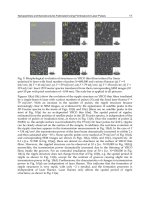
Irrespective on the substrate we used, the obtained films show a smooth surface with very
low-density or no particulates at all, as indicated by scanning electron microscopy analysis,
see Fig. 2a. Their morphology (as revealed by atomic force microscopy, AFM, Fig. 2b)
consists of compact quasispherical crystallites with typical dimensions (root mean square
roughness) between 5 and 15 nm. The non-dependence of film morphology on the substrate
nature may be an indication that the growth mechanism is governed mainly by the laser
beam/ target interaction.
a. b.
Fig. 2. a) SEM image of a VO
2
thin film growth on a sapphire substrate showing a smooth
surface and b) AFM image obtained on a VO
2
film (75-nm thickness) onto a sapphire R
substrate showing compact crystallites.
Fig. 3. Typical XRD scan for a 200-nm thick VO
2
thin film deposited on an Al
2
O
3
(C)
substrate showing characteristic peaks ((020) and (040) of the monoclinic phase of VO
2
.
Exploitingthesemiconductor-metalphasetransitionofVO2materials:anovel
directiontowardstuneabledevicesandsystemsforRFmicrowaveapplications 39
proposed an original approach for the design and fabrication of self-resetting power limiting
devices based on microwave power induced SMT in vanadium dioxide (Givernaud et al.,
2009). As an illustration of our current activities towards the integration of VO
2
layers in RF-
microwave (RF- MW) devices, we will present the design, fabrication and caracterization of
thermally activated MW switches and their integration in a new type of thermally triggered
reconfigurable 4-bit band stop filter designed to operate in the 9- 11 GHz frequency range.
3. PLD deposition and structural, optical and electrical characterization of the
VO
2
thin films
Several deposition methods have been proposed for fabrication of VO
2
thin films:
sputtering, evaporation pyrolysis or chemical reaction techniques (Hood & DeNatale, 1991;
Stotz et al., 1999; Manning et al., 2002; Li et al., 2008 etc.). According to the multivalency of
vanadium ion and its complex oxide structure (Griffiths & Eastwood, 1974), numerous
phases with stoechiometries close to VO
2
can exist (from V
4
O to V
2
O
5
) and the synthesis of
phase pure VO
2
thin films is an important challenge. Reactive pulsed laser deposition (PLD)
is a suitable technique for obtaining high-purity oxide thin films (Chrisey & Hubler, 1994;
Eason, 2007), very well adapted for obtaining the stoichiometric VO
2
layers. However,
careful optimisation of the working parameters is necessary to obtain thin films of the pure
VO
2
stabilized phase without any post-treatment.
Fig. 1. Photography of the PLD set-up showing schematically the inside of the deposition
chamber (left-hand side) and the expansion of the plasma plume towards the substrate after
the laser pulse (right-hand side).
In our case, VO
2
thin films were deposited using reactive pulsed laser deposition from a
high purity grade (99.95%) vanadium metal target under an oxygen atmosphere. The
experimental set-up (picture shown in Fig.1) was described elsewhere (Dumas-Bouchiat et
al., 2006) and is based on an excimer KrF laser (with a wavelength of 248 nm and a pulse
duration of 25 ns), operating at a repetition rate of 10 Hz. The laser beam is focused on a
rotating target in order to obtain fluences (i.e. energies per irradiated surface unit) in the
order of 5 to 9 J/cm². The plasma plume expands in the ambient oxygen atmosphere (total
pressure in the chamber maintained at 2×10
-2
mbar). Since it has a relatively low lattice
parameter mismatch (4.5%) as compared to VO
2
monoclinic phase, monocristalline Al
2
O
3
(C)
is a good candidate to deposit mono-oriented VO
2
films (Garry et al., 2004). The substrate is
heated by an halogen lamp at about 500°C and the deposition duration is changing from 10
to 45 minutes leading to thickness in the range 100 - 600 nm. VO
2
thin films have been also
deposited on sapphire R-type substrates (Al
2
O
3
(R)), quartz or 100 Si substrates (bare or
oxidized with a 1-m thick layer of SiO
2
).
Irrespective on the substrate we used, the obtained films show a smooth surface with very
low-density or no particulates at all, as indicated by scanning electron microscopy analysis,
see Fig. 2a. Their morphology (as revealed by atomic force microscopy, AFM, Fig. 2b)
consists of compact quasispherical crystallites with typical dimensions (root mean square
roughness) between 5 and 15 nm. The non-dependence of film morphology on the substrate
nature may be an indication that the growth mechanism is governed mainly by the laser
beam/ target interaction.
a. b.
Fig. 2. a) SEM image of a VO
2
thin film growth on a sapphire substrate showing a smooth
surface and b) AFM image obtained on a VO
2
film (75-nm thickness) onto a sapphire R
substrate showing compact crystallites.
Fig. 3. Typical XRD scan for a 200-nm thick VO
2
thin film deposited on an Al
2
O
3
(C)
substrate showing characteristic peaks ((020) and (040) of the monoclinic phase of VO
2
.
AdvancedMicrowaveandMillimeterWave
Technologies:SemiconductorDevices,CircuitsandSystems40
X-Ray diffraction -XRD investigations (in θ, 2θ configuration) performed on VO
2
/Al
2
O
3
(C)
thin films reveal two peaks located near 40.2° and 86.8° corresponding respectively to the
(020) and (040) planes of the monoclinic VO
2
phase. In certain cases, and especially for
amorphous substrates (SiO
2
/ Si substrates), depending on the deposition parameters, a peak
appears near 28° corresponding to the (011) planes of VO
2
with an orthorhombic structure
(Youn et al., 2004).
3.1 Temperature-induced SMT of VO
2
thin films
For the obtained VO
2
films we recorded the variation of their electrical optical and
properties (resistivity and optical transmission variation) with the applied temperature in
order to rapidly assess the amplitude of their temperature-activated SMT transition.
The electrical resistance/ resistivity of the VO
2
thin films was recorded in the 20-100°C
temperature range using a two-terminal device (two metallic contacts deposited nearby on a
rectangular VO
2
pattern). A typical resistance hysteresis cycle (heating- cooling loop) of a
200-nm thick VO
2
thin films deposited on a C-type sapphire substrate can be observed in
Fig. 4 (the VO2 pattern between the two measurements electrodes was, in this case, 70 m
long x 45 m wide and 200 nm thick). One may observe a huge change in its resistance as
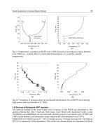
the temperature is cycled through the phase transition (R~ 450 k at 20°C down to R·
at 100°C). The width of the hysteresys curve (heating- cooling cycle) is very small: the
transition occurs in the 72-74°C range when heating the sample (transformation from
semiconductor to metal) and in the 65-68°C range when cooling down at room temperature,
and is witnessing on the high quality of the obtained material.
Fig. 4. Resistance variation with temperature for a VO
2
film (two terminal device of 70 mm
long, 45 mm wide and 200 nm thick) fabricated by PLD on a C-type sapphire substrate
The optical transmission measurements of VO
2
layers on different substrates as a function of
the temperature were done in the UV-visible- mid-IR regions of the spectrum using a Varian
Carry 5000 spectrophotometer equipped with a sample heater. They were recorded for
different temperatures in the 20-100° C domain. As observed on Fig. 5, the VO
2
films
deposited on Al2O3 (R) and on SiO
2
/ Si substrates showed a very sharp phase transition
witnessing of abrupt change (transmission change factors between 4 and 8) of its optical
properties (drastic modification of its refractive index and absorption coefficient). One may
notice on the graph on Fig. 5a that the temperature- dependent transmission curves intersect
in a particular point, the isosbestic point (at ~850 nm) where the transmittance is constant
for all temperatures (Qazilbash et al., 2007).
a.
b.
Fig. 5. Optical transmission spectra vs. temperature for 50-nm thick VO
2
films made by PLD
on R-type sapphire substrates (a) and 1-m thick SiO
2
/ Si substrate (the oscillations visible
on these spectra are interference patterns due to the SiO
2
/ Si stack layers)(b).
We also investigated the reflectivity variation of the VO
2
films versus the temperature.
Typically, a substrate covered with a VO
2
thin layer was placed on a heating stage and the
optical power of a reflected fiber laser beam (at 1550 nm) directed at almost normal
incidence onto the film surface was recorded during temperature variation in the 20-100°C
domain. On Fig. 6 is presented a typical hysteresys cycle of film’s reflectivity (heating-
cooling cycle). The VO
2
films showed a very sharp, abrupt phase transition that occurs
Exploitingthesemiconductor-metalphasetransitionofVO2materials:anovel
directiontowardstuneabledevicesandsystemsforRFmicrowaveapplications 41
X-Ray diffraction -XRD investigations (in θ, 2θ configuration) performed on VO
2
/Al
2
O
3
(C)
thin films reveal two peaks located near 40.2° and 86.8° corresponding respectively to the
(020) and (040) planes of the monoclinic VO
2
phase. In certain cases, and especially for
amorphous substrates (SiO
2
/ Si substrates), depending on the deposition parameters, a peak
appears near 28° corresponding to the (011) planes of VO
2
with an orthorhombic structure
(Youn et al., 2004).
3.1 Temperature-induced SMT of VO
2
thin films
For the obtained VO
2
films we recorded the variation of their electrical optical and
properties (resistivity and optical transmission variation) with the applied temperature in
order to rapidly assess the amplitude of their temperature-activated SMT transition.
The electrical resistance/ resistivity of the VO
2
thin films was recorded in the 20-100°C
temperature range using a two-terminal device (two metallic contacts deposited nearby on a
rectangular VO
2
pattern). A typical resistance hysteresis cycle (heating- cooling loop) of a
200-nm thick VO
2
thin films deposited on a C-type sapphire substrate can be observed in
Fig. 4 (the VO2 pattern between the two measurements electrodes was, in this case, 70 m
long x 45 m wide and 200 nm thick). One may observe a huge change in its resistance as
the temperature is cycled through the phase transition (R~ 450 k at 20°C down to R·
at 100°C). The width of the hysteresys curve (heating- cooling cycle) is very small: the
transition occurs in the 72-74°C range when heating the sample (transformation from
semiconductor to metal) and in the 65-68°C range when cooling down at room temperature,
and is witnessing on the high quality of the obtained material.
Fig. 4. Resistance variation with temperature for a VO
2
film (two terminal device of 70 mm
long, 45 mm wide and 200 nm thick) fabricated by PLD on a C-type sapphire substrate
The optical transmission measurements of VO
2
layers on different substrates as a function of
the temperature were done in the UV-visible- mid-IR regions of the spectrum using a Varian
Carry 5000 spectrophotometer equipped with a sample heater. They were recorded for
different temperatures in the 20-100° C domain. As observed on Fig. 5, the VO
2
films
deposited on Al2O3 (R) and on SiO
2
/ Si substrates showed a very sharp phase transition
witnessing of abrupt change (transmission change factors between 4 and 8) of its optical
properties (drastic modification of its refractive index and absorption coefficient). One may
notice on the graph on Fig. 5a that the temperature- dependent transmission curves intersect
in a particular point, the isosbestic point (at ~850 nm) where the transmittance is constant
for all temperatures (Qazilbash et al., 2007).
a.
b.
Fig. 5. Optical transmission spectra vs. temperature for 50-nm thick VO
2
films made by PLD
on R-type sapphire substrates (a) and 1-m thick SiO
2
/ Si substrate (the oscillations visible
on these spectra are interference patterns due to the SiO
2
/ Si stack layers)(b).
We also investigated the reflectivity variation of the VO
2
films versus the temperature.
Typically, a substrate covered with a VO
2
thin layer was placed on a heating stage and the
optical power of a reflected fiber laser beam (at 1550 nm) directed at almost normal
incidence onto the film surface was recorded during temperature variation in the 20-100°C
domain. On Fig. 6 is presented a typical hysteresys cycle of film’s reflectivity (heating-
cooling cycle). The VO
2
films showed a very sharp, abrupt phase transition that occurs
AdvancedMicrowaveandMillimeterWave
Technologies:SemiconductorDevices,CircuitsandSystems42
irrespective of the used substrate or of their thickness. As in the case of the electrical
resistivity measurements, the width of the hysteresys curve is very small.
Fig. 6. Hysteresis cycle of reflectivity (at 1550 nm) vs. temperature for a 75-nm thick VO
2
film
made by PLD on C-type sapphire substrate showing the sharp phase transition of the VO
2
material.
3.2 Electrically- induced SMT of VO
2
thin films
The proof of concept of thermally induced SMT of VO
2
thin films for realising microwave
(and optical) switching devices shown above represents already an innovative, interesting
field of research both from theoretically and practical points of view. However, the
electrically driven SMT of the VO
2
material will results in more practical devices (without
the need of a additional temperature source for the phase transition activation) that,
theoretically, can be activated several orders of magnitude faster (Mott, 1968; Cavalleri et al.,
2001; Stefanovich et al., 2000; Kim et al., 2004).
We therefore initiated investigations for evaluating the electrically induced phase transition
of VO
2
thin films integrated in two-terminal switching devices. The VO
2
pattern is included
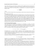
in an electrical circuit (Fig. 7a) with a c.c. voltage source (applied voltage, V
ap
), an
amperemeter (measuring the current in the circuit, I) and a resistor (Rs, with typical values
between 100 and 1500 ) for limiting the overall current in the circuit since high values of
the current may damage the VO
2
switch. The first results (I-V
ap
and I-V
VO2
characteristics) of
the electrically actuated VO
2
- based two-terminal device (rectangular pattern, 40- m long,
95–m wide and 200 nm thick) are presented on Figs. 7 b, c. It may be seen that at a given
threshold voltage (V
ap
between 11 and 14 V for the c.c. voltage source, and V
VO2
~ 10.5 to 13
V for the voltage on the VO
2
circuit, depending on the Rs value) the current increase
abruptly, indicating that the resistivity of the VO
2
layer decreased. This phenomenon is
indicative on the onset of the phase transition, VO
2
passes from a high resistive state
(semiconductor) in a low-resistive one (it becomes metallic).
a.
b.
c.
Fig. 7. a) Electrical circuit set-up for investigating the Electrically- induced SMT transition of
a two terminal switching device based on a VO
2
thin film (200-nm thick on C-type sapphire);
b) I-V
ap
hysteresis characteristic as the V
ap
is swept between 0 and maximum of 30V and
backwards and c) the typical S-shape of the I-V
VO2
characteristic of the device.
The nonlinear, S-shaped, negative differential resistance (NDR) I-V
VO2
characteristic, typical
for the VO
2
material (and whose shape can be tuned with external applied temperature) is of
high interest from the viewpoint of fundamental physics as well as of a broad range of
applications (NDR based oscillators, transistors, filters etc.).
Exploitingthesemiconductor-metalphasetransitionofVO2materials:anovel
directiontowardstuneabledevicesandsystemsforRFmicrowaveapplications 43
irrespective of the used substrate or of their thickness. As in the case of the electrical
resistivity measurements, the width of the hysteresys curve is very small.
Fig. 6. Hysteresis cycle of reflectivity (at 1550 nm) vs. temperature for a 75-nm thick VO
2
film
made by PLD on C-type sapphire substrate showing the sharp phase transition of the VO
2
material.
3.2 Electrically- induced SMT of VO
2
thin films
The proof of concept of thermally induced SMT of VO
2
thin films for realising microwave
(and optical) switching devices shown above represents already an innovative, interesting
field of research both from theoretically and practical points of view. However, the
electrically driven SMT of the VO
2
material will results in more practical devices (without
the need of a additional temperature source for the phase transition activation) that,
theoretically, can be activated several orders of magnitude faster (Mott, 1968; Cavalleri et al.,
2001; Stefanovich et al., 2000; Kim et al., 2004).
We therefore initiated investigations for evaluating the electrically induced phase transition
of VO
2
thin films integrated in two-terminal switching devices. The VO
2
pattern is included
in an electrical circuit (Fig. 7a) with a c.c. voltage source (applied voltage, V
ap
), an
amperemeter (measuring the current in the circuit, I) and a resistor (Rs, with typical values
between 100 and 1500 ) for limiting the overall current in the circuit since high values of
the current may damage the VO
2
switch. The first results (I-V
ap
and I-V
VO2
characteristics) of
the electrically actuated VO
2
- based two-terminal device (rectangular pattern, 40- m long,
95–m wide and 200 nm thick) are presented on Figs. 7 b, c. It may be seen that at a given
threshold voltage (V
ap
between 11 and 14 V for the c.c. voltage source, and V
VO2
~ 10.5 to 13
V for the voltage on the VO
2
circuit, depending on the Rs value) the current increase
abruptly, indicating that the resistivity of the VO
2
layer decreased. This phenomenon is
indicative on the onset of the phase transition, VO
2
passes from a high resistive state
(semiconductor) in a low-resistive one (it becomes metallic).
a.
b.
c.
Fig. 7. a) Electrical circuit set-up for investigating the Electrically- induced SMT transition of
a two terminal switching device based on a VO
2
thin film (200-nm thick on C-type sapphire);
b) I-V
ap
hysteresis characteristic as the V
ap
is swept between 0 and maximum of 30V and
backwards and c) the typical S-shape of the I-V
VO2
characteristic of the device.
The nonlinear, S-shaped, negative differential resistance (NDR) I-V
VO2
characteristic, typical
for the VO
2
material (and whose shape can be tuned with external applied temperature) is of
high interest from the viewpoint of fundamental physics as well as of a broad range of
applications (NDR based oscillators, transistors, filters etc.).
AdvancedMicrowaveandMillimeterWave
Technologies:SemiconductorDevices,CircuitsandSystems44
The device remains in the activated state as long as the voltage or the current is maintained
in the circuit. For evaluating the switching time of the electrically induced transition we
used a similar activation schema (Fig. 8a) but including an a.c. voltage actuation with a
square-type waveform (voltage pulses for which the temporal width were varied from 1 to
20 m).
a.
b.
Fig. 8. a) Set-up for electrical activation of the SMT transition and evaluation of the
switching time of a VO
2
-based two-terminal switch b) applied squared waveform (16 V
amplitude, 1.5 s in width) and the voltage variation through the VO2 switch (in series with
a resistor having R
S
= 278 ) showing installation of the VO2's SMT with activation times
which varies between 100 and 250 ns.
As indicated in Fig. 8 b, c, preliminary results indicate switching times values as low as
several hundreds of nano-seconds, which are, however, situated well above the
electronically induced VO
2
transition (supposed to occur in the ps domain).
Although the theoretical calculations for a current-induced temperature initiation of the
SMT transition (by the Joule heating effect) on the tested device lies in the order of the
micro-second scale time (higher than the switching times we recorded), it is prematurely to
asses on a purely electrical-induced phase transition (by charge injection). More likely we
recorded a switching time describing a mixture of the two potentially present mechanisms
(Joule effect heating and charge injection). Nevertheless, the key point of these experiments
is that the switching time values are better than those of devices employing fast MEMS-
based solutions (Lacroix et al., 2007) and not far from the switching times values of the
semiconductors currently used in millimeter domain-switching devices.
We should point out that the electrical activation of VO
2
thin films is also accompanied by
changes in their optical properties, easily perceived using optical microscopy and recorded
using a CCD camera, as reflectivity change periodically with the applied a.c. signal. These
findings are currently exploited in our group for fabrication of variable reflectivity micro
mirrors and attenuators in the optical domain for high-speed modulators in novel laser
systems (results not reported here).
To resume the preliminary results presented above we may say that the VO
2
is a very
interesting and exciting phase transition material. Its electrical and optical properties may be
tuned in a static or dynamical way by external factors such as the temperature or an applied
electrical field or voltage. These results were further exploited for the realization of rapid
electrically switching of microwave coplanar waveguide (CPW) lines or the fabrication of
band-stop-type MW filters.
4. Integration of VO
2
thin films in microwave switches and filters
The enormous resistivity change (3 to 4 order of magnitude) of the VO
2
material undergoing
the SMT induced by the temperature or by an applied voltage was exploited to fabricate and
characterize simple microwave switches based on a coplanar microwave waveguide
integrating VO
2
thin films. We obtained temperature activated switching functions (in both
shunt and series configurations) with relatively low losses and more than 25 dB
transmission variations between the ON/OFF states, on a very large bandwidth (50 MHz–
35 GHz) (Crunteanu et al., 2007; Dumas-Bouchiat et al., 2009). The concept was successfully
implemented for more complex devices, such as tuneable band stop filters operating around
10 GHz in the microwave frequency domain (Givernaud et al., 2008).
4.1 Microwave switching based on VO
2
films two terminal devices
In the followings we will present a novel concept of VO
2
-based electrical switch by using the
discrete (and local) thermal activation of a VO2 two-terminal device using a miniature
heating element. The micro-heater is based on a thin-film resistor fabricated from a Ni-
doped tetrahedral carbon layer (Ni:ta-C). Nickel-doped ta-C layers are currently used in our
laboratory and efficiently integrated in radio frequency micro electro mechanical systems
(RF MEMS) and in other tunable components (Orlianges et al., 2005). These thin films allows
the realization of localized, high value, planar, easily patterned resistances, leading to
significant improvement of insertion losses of MEMS switches integrated in electronic
devices. Such thin-film resistors are often used under high value of electrical current, which
generate important heating of these devices. Our previous investigations on ta-C layers
doped with 5%- 30% wt. Ni showed that the layers preserve their integrity for current
Exploitingthesemiconductor-metalphasetransitionofVO2materials:anovel
directiontowardstuneabledevicesandsystemsforRFmicrowaveapplications 45
The device remains in the activated state as long as the voltage or the current is maintained
in the circuit. For evaluating the switching time of the electrically induced transition we
used a similar activation schema (Fig. 8a) but including an a.c. voltage actuation with a
square-type waveform (voltage pulses for which the temporal width were varied from 1 to
20 m).
a.
b.
Fig. 8. a) Set-up for electrical activation of the SMT transition and evaluation of the
switching time of a VO
2
-based two-terminal switch b) applied squared waveform (16 V
amplitude, 1.5 s in width) and the voltage variation through the VO2 switch (in series with
a resistor having R
S
= 278 ) showing installation of the VO2's SMT with activation times
which varies between 100 and 250 ns.
As indicated in Fig. 8 b, c, preliminary results indicate switching times values as low as
several hundreds of nano-seconds, which are, however, situated well above the
electronically induced VO
2
transition (supposed to occur in the ps domain).
Although the theoretical calculations for a current-induced temperature initiation of the
SMT transition (by the Joule heating effect) on the tested device lies in the order of the
micro-second scale time (higher than the switching times we recorded), it is prematurely to
asses on a purely electrical-induced phase transition (by charge injection). More likely we
recorded a switching time describing a mixture of the two potentially present mechanisms
(Joule effect heating and charge injection). Nevertheless, the key point of these experiments
is that the switching time values are better than those of devices employing fast MEMS-
based solutions (Lacroix et al., 2007) and not far from the switching times values of the
semiconductors currently used in millimeter domain-switching devices.
We should point out that the electrical activation of VO
2
thin films is also accompanied by
changes in their optical properties, easily perceived using optical microscopy and recorded
using a CCD camera, as reflectivity change periodically with the applied a.c. signal. These
findings are currently exploited in our group for fabrication of variable reflectivity micro
mirrors and attenuators in the optical domain for high-speed modulators in novel laser
systems (results not reported here).
To resume the preliminary results presented above we may say that the VO
2
is a very
interesting and exciting phase transition material. Its electrical and optical properties may be
tuned in a static or dynamical way by external factors such as the temperature or an applied
electrical field or voltage. These results were further exploited for the realization of rapid
electrically switching of microwave coplanar waveguide (CPW) lines or the fabrication of
band-stop-type MW filters.
4. Integration of VO
2
thin films in microwave switches and filters
The enormous resistivity change (3 to 4 order of magnitude) of the VO
2
material undergoing
the SMT induced by the temperature or by an applied voltage was exploited to fabricate and
characterize simple microwave switches based on a coplanar microwave waveguide
integrating VO
2
thin films. We obtained temperature activated switching functions (in both
shunt and series configurations) with relatively low losses and more than 25 dB
transmission variations between the ON/OFF states, on a very large bandwidth (50 MHz–
35 GHz) (Crunteanu et al., 2007; Dumas-Bouchiat et al., 2009). The concept was successfully
implemented for more complex devices, such as tuneable band stop filters operating around
10 GHz in the microwave frequency domain (Givernaud et al., 2008).
4.1 Microwave switching based on VO
2
films two terminal devices
In the followings we will present a novel concept of VO
2
-based electrical switch by using the
discrete (and local) thermal activation of a VO2 two-terminal device using a miniature
heating element. The micro-heater is based on a thin-film resistor fabricated from a Ni-
doped tetrahedral carbon layer (Ni:ta-C). Nickel-doped ta-C layers are currently used in our
laboratory and efficiently integrated in radio frequency micro electro mechanical systems
(RF MEMS) and in other tunable components (Orlianges et al., 2005). These thin films allows
the realization of localized, high value, planar, easily patterned resistances, leading to
significant improvement of insertion losses of MEMS switches integrated in electronic
devices. Such thin-film resistors are often used under high value of electrical current, which
generate important heating of these devices. Our previous investigations on ta-C layers
doped with 5%- 30% wt. Ni showed that the layers preserve their integrity for current
AdvancedMicrowaveandMillimeterWave
Technologies:SemiconductorDevices,CircuitsandSystems46
densities as high as 1.5.10
5
A/cm
2
(Orlianges et al., 2004). This caracteristic of the Ni:ta-C
layers can be exploited for fabrication of localized, micrometer-range heating elements
which may be used to discretely activate VO
2
-based two terminal switches (the important
ammount of heat generated into the Ni:ta-C layers will be transmitted to the VO2 patterns
placed underneath). The amount of the heat generated by the micro heater element can be
adjusted by changing the dimensions and the doping level of the Ni:ta-C pattern.
The design of a fabricated VO
2
-based switch which can be activated by the heat generated in
a Ni:ta-C thin film is presented in the optical micrscope image on Fig. 9 a.
a.
b.
Fig. 9. a) Optical microscopy image of a VO
2
-based two terminal switch (400-m long, 200-
m wide, 200-nm thick pattern between two gold electrodes) which is activated by the
current induced heating in a 10% wt. Ni:ta-C pattern situated above it (340-m long, 150-m
wide and 100-nm thick) and b) optical images showing the sequential activation (phase
transition) of the underneath VO
2
layer when applying periodical squared voltage pulses
(80V amplitude, 1Hz) on the Ni:ta-C pattern (VO
2
-S-semiconducting phase and VO
2
-M – the
mettalic state of the VO
2
layer.
The device was fabricated in a clean room environment using classical micro fabrication
technology. The 200-nm thick VO
2
films were deposited using PLD from a vanadium target
in oxygen atmosphere on C-cut sapphire substrates (500-m thickness) in the conditions
described above. The VO2 layers were further patterned using optical lithography and wet
etching for defining the rectangular patterns. It follows the partial masking of the substrate
with a photoresist layer for deposition of the Ni:ta-C layers (~100-nm thick) precisely above
the VO
2
patterns (the lift-off technique). The nickel doped ta-C films have been deposited
under high vacuum by KrF laser ablation of alternating C and Ni targets at ambient
temperature (Orlianges et al., 2004). At the end, we fabricated the metallic electrodes: a Ti/
Au layer (6-nm/ 1-m thick Ti is used as adhesion layer) is deposited using thermal
evaporation; the shape of the electrodes are defined by photoresist masking using optical
lithography followed by the partial wet etching of the Ti/ Au layer. We tested different
pattern dimensions for the VO2 switch (from 200 to 400-m long and 100 to 200-m wide)
and for the heating Ni:ta-C thin film resistors (100 to 350-m long and 50 to 150-m wide).
For the device shown in Fig. 9 a (VO
2
pattern of 400-m long, 200-m wide, 200-nm thick
pattern between the two metallic electrodes), when applying a current (up to 10 mA) to the
Ni:ta-C heating element (340-m long, 150-m wide, with an overall resistance of ~11 k)
the heat generated in the micro-heater will dissipate to the underneath VO
2
layer and will
raise its temperature above the SMT’s transition temperature (around 68°C). The VO
2
will
therefore pass from a semiconductor to a metal state. As in the case of an optical switch, the
transition is easily observed using the optical microscopy as clear changes of the VO
2
layer’s
reflectivity. These sequential reflectivity changes were recorded using a CCD camera (Fig. 9
b) as we applied to the micro heating layer (Ni:ta-C) a pulsed periodical squared signal (80V
amplitude, 1Hz). The onset of the VO
2
’s phase transition was also recorded electrically by
monitoring the resistance of the two-terminal device as a c.c. voltage was progressively
applied on the Ni:ta-C heater (Fig. 10).
Fig. 10. VO
2
’s two-terminal device transversal resistance versus the voltage applied on the
Ni:ta-C heating resistance: heating phase (red), cooling phase (blue)
One may easily noticed the great variation of the VO
2
’s resistivity (onset of the SMT) as the
Ni:ta-C element dissipate the resistive heating. Work is in progress in order to simulate the
heating transfer processes in the overall device, which will allow for optimum design in
term of lowering the power consumption. The obtained thermal switching device allows for
discrete, localized activation of micrometer-sized VO
2
patterns and may be easily integrated
Exploitingthesemiconductor-metalphasetransitionofVO2materials:anovel
directiontowardstuneabledevicesandsystemsforRFmicrowaveapplications 47
densities as high as 1.5.10
5
A/cm
2
(Orlianges et al., 2004). This caracteristic of the Ni:ta-C
layers can be exploited for fabrication of localized, micrometer-range heating elements
which may be used to discretely activate VO
2
-based two terminal switches (the important
ammount of heat generated into the Ni:ta-C layers will be transmitted to the VO2 patterns
placed underneath). The amount of the heat generated by the micro heater element can be
adjusted by changing the dimensions and the doping level of the Ni:ta-C pattern.
The design of a fabricated VO
2
-based switch which can be activated by the heat generated in
a Ni:ta-C thin film is presented in the optical micrscope image on Fig. 9 a.
a.
b.
Fig. 9. a) Optical microscopy image of a VO
2
-based two terminal switch (400-m long, 200-
m wide, 200-nm thick pattern between two gold electrodes) which is activated by the
current induced heating in a 10% wt. Ni:ta-C pattern situated above it (340-m long, 150-m
wide and 100-nm thick) and b) optical images showing the sequential activation (phase
transition) of the underneath VO
2
layer when applying periodical squared voltage pulses
(80V amplitude, 1Hz) on the Ni:ta-C pattern (VO
2
-S-semiconducting phase and VO
2
-M – the
mettalic state of the VO
2
layer.
The device was fabricated in a clean room environment using classical micro fabrication
technology. The 200-nm thick VO
2
films were deposited using PLD from a vanadium target
in oxygen atmosphere on C-cut sapphire substrates (500-m thickness) in the conditions
described above. The VO2 layers were further patterned using optical lithography and wet
etching for defining the rectangular patterns. It follows the partial masking of the substrate
with a photoresist layer for deposition of the Ni:ta-C layers (~100-nm thick) precisely above
the VO
2
patterns (the lift-off technique). The nickel doped ta-C films have been deposited
under high vacuum by KrF laser ablation of alternating C and Ni targets at ambient
temperature (Orlianges et al., 2004). At the end, we fabricated the metallic electrodes: a Ti/
Au layer (6-nm/ 1-m thick Ti is used as adhesion layer) is deposited using thermal
evaporation; the shape of the electrodes are defined by photoresist masking using optical
lithography followed by the partial wet etching of the Ti/ Au layer. We tested different
pattern dimensions for the VO2 switch (from 200 to 400-m long and 100 to 200-m wide)
and for the heating Ni:ta-C thin film resistors (100 to 350-m long and 50 to 150-m wide).
For the device shown in Fig. 9 a (VO
2
pattern of 400-m long, 200-m wide, 200-nm thick
pattern between the two metallic electrodes), when applying a current (up to 10 mA) to the
Ni:ta-C heating element (340-m long, 150-m wide, with an overall resistance of ~11 k)
the heat generated in the micro-heater will dissipate to the underneath VO
2
layer and will
raise its temperature above the SMT’s transition temperature (around 68°C). The VO
2
will
therefore pass from a semiconductor to a metal state. As in the case of an optical switch, the
transition is easily observed using the optical microscopy as clear changes of the VO
2
layer’s
reflectivity. These sequential reflectivity changes were recorded using a CCD camera (Fig. 9
b) as we applied to the micro heating layer (Ni:ta-C) a pulsed periodical squared signal (80V
amplitude, 1Hz). The onset of the VO
2
’s phase transition was also recorded electrically by
monitoring the resistance of the two-terminal device as a c.c. voltage was progressively
applied on the Ni:ta-C heater (Fig. 10).
Fig. 10. VO
2
’s two-terminal device transversal resistance versus the voltage applied on the
Ni:ta-C heating resistance: heating phase (red), cooling phase (blue)
One may easily noticed the great variation of the VO
2
’s resistivity (onset of the SMT) as the
Ni:ta-C element dissipate the resistive heating. Work is in progress in order to simulate the
heating transfer processes in the overall device, which will allow for optimum design in
term of lowering the power consumption. The obtained thermal switching device allows for
discrete, localized activation of micrometer-sized VO
2
patterns and may be easily integrated
AdvancedMicrowaveandMillimeterWave
Technologies:SemiconductorDevices,CircuitsandSystems48
in more complex functions (filtering module), as it will be demonstrated in the next sub-
chapter.
4.2 Design and performances of tuneable band-stop filters including VO
2
-based
switches.
We used the large resistivity change of the device presented above for realising a tuneable 4-
pole band stop filter designed to operate in the 9- 11 GHz frequency range with a large
signal attenuation in the attenuated band (> 20 dB) (Givernaud et al., 2008). The filter
(realised in the micro strip geometry) consists in a 50 transmission line coupled with four
U-shaped resonators (Fig. 11). Each resonator is "closed" by a VO
2
-based pattern which can
be independently activated from the semiconductor to the metallic phase by the Ni:ta-C thin
film micro heater. At room temperature, the VO
2
patterns are insulating (VO
2
pattern
resistance of 98 k), the resonators are “opened” and each of them will introduce a specific
absorption band in the transmission spectrum of the filter (Fig. 13 a). The design of the filter
was done using the ADS Momentum simulator and the dimensions and position of each of
the resonators (position and distance from the transmission line) was optimised in such a
way that the sum of each absorption band result in an broad absorption band between 10
and 11 GHz while maintaining a high signal attenuation (> 20 dB), as visualized in Fig. 13 a.
Fig. 11. Design of the four-pole band stop filter that can be discretely tuned by thermally
activated each of the VO
2
-charged resonators; the insert shows the design of the VO
2
-based
switch (activated by a Ni:ta-C pattern) which was adapted to the filter’s design.
When individually activated, the metallic VO
2
pattern (resistance of 78 ) will electrically
closed its corresponding U-shaped resonator. The design of the filter (dimensions,
resonators dimensions etc.) was done in such a way that the absorption band of the
activated resonator would be then shifted far away from the operation frequency band of
the filter. The response of the filter will change: shift of the absorption band (tuneability),
bandwidth decrease and even disappearance of the attenuation band (Fig. 13 b when all the
resonators are activated). This concept was already applied (Givernaud et al., 2008; Dumas-
Bouchiat et al., 2009) and results in innovative, discretely tuned filtering functions in the
microwave domain.
The filter was fabricated in a clean room environment using classical micro fabrication
technology in the conditions described elsewhere (Givernaud et al., 2008). The obtained
device was placed using a conductive epoxy paste (for defining the ground plane of the
micro strip geometry) in a metallic package and the transmission line ends are electrically
connected to SMA-type connectors for measurements (Fig. 12).
Fig. 12. Photography of the realized VO
2
-based four-pole filter inserted in a metallic housing
and connected to SMA connectors for measuring its response.
a.
Exploitingthesemiconductor-metalphasetransitionofVO2materials:anovel
directiontowardstuneabledevicesandsystemsforRFmicrowaveapplications 49
in more complex functions (filtering module), as it will be demonstrated in the next sub-
chapter.
4.2 Design and performances of tuneable band-stop filters including VO
2
-based
switches.
We used the large resistivity change of the device presented above for realising a tuneable 4-
pole band stop filter designed to operate in the 9- 11 GHz frequency range with a large
signal attenuation in the attenuated band (> 20 dB) (Givernaud et al., 2008). The filter
(realised in the micro strip geometry) consists in a 50 transmission line coupled with four
U-shaped resonators (Fig. 11). Each resonator is "closed" by a VO
2
-based pattern which can
be independently activated from the semiconductor to the metallic phase by the Ni:ta-C thin
film micro heater. At room temperature, the VO
2
patterns are insulating (VO
2
pattern
resistance of 98 k), the resonators are “opened” and each of them will introduce a specific
absorption band in the transmission spectrum of the filter (Fig. 13 a). The design of the filter
was done using the ADS Momentum simulator and the dimensions and position of each of
the resonators (position and distance from the transmission line) was optimised in such a
way that the sum of each absorption band result in an broad absorption band between 10
and 11 GHz while maintaining a high signal attenuation (> 20 dB), as visualized in Fig. 13 a.
Fig. 11. Design of the four-pole band stop filter that can be discretely tuned by thermally
activated each of the VO
2
-charged resonators; the insert shows the design of the VO
2
-based
switch (activated by a Ni:ta-C pattern) which was adapted to the filter’s design.
When individually activated, the metallic VO
2
pattern (resistance of 78 ) will electrically
closed its corresponding U-shaped resonator. The design of the filter (dimensions,
resonators dimensions etc.) was done in such a way that the absorption band of the
activated resonator would be then shifted far away from the operation frequency band of
the filter. The response of the filter will change: shift of the absorption band (tuneability),
bandwidth decrease and even disappearance of the attenuation band (Fig. 13 b when all the
resonators are activated). This concept was already applied (Givernaud et al., 2008; Dumas-
Bouchiat et al., 2009) and results in innovative, discretely tuned filtering functions in the
microwave domain.
The filter was fabricated in a clean room environment using classical micro fabrication
technology in the conditions described elsewhere (Givernaud et al., 2008). The obtained
device was placed using a conductive epoxy paste (for defining the ground plane of the
micro strip geometry) in a metallic package and the transmission line ends are electrically
connected to SMA-type connectors for measurements (Fig. 12).
Fig. 12. Photography of the realized VO
2
-based four-pole filter inserted in a metallic housing
and connected to SMA connectors for measuring its response.
a.
AdvancedMicrowaveandMillimeterWave
Technologies:SemiconductorDevices,CircuitsandSystems50
b.
Fig. 13. a) ADS Momentum simulation of the S21 transmission parameter for the overall
filter (red curve), showing the absorption band contributions of each resonators and b) the
simulated S
21
transmission parameter of the four-pole band stop filter when the VO
2
-based
resonators are "opened" (red curve, VO
2
-SC) and "closed" (blue curve, VO
2
-metal).
The response of the packaged filter was measured using a calibrated four-ports vectorial
network analyser (VNA, HP 8722 ES) in the 7 to 14 GHz frequencies range. The measured
response of the filter is presented on the graph in Fig. 14 in the two extreme cases: when all
the VO
2
patterns are insulating, red curve, and when all the VO
2
patterns are activated by
the Ni:ta-C micro-heating elements.
Fig. 14. Measured responses (transmission S21 parameter) of the four pole band stop filter,
at room temperature (red curve VO2-SC) and activated (blue curve, VO2-metal, all of the
resonators are activated)
One may notice a good agreement of the measured filter responses with the simulations
(Fig. 13b). Although the operation band is shifted towards the low frequencies this can be
easily corrected for future design by taking into account the deviation from the theoretical
values of the materials constants used for the simulation response and by taking care to the
micro fabrication tolerances).The tunability of the filter can be demonstrated by individual
activation (using the micro-heaters) of specific resonators. When the VO
2
-switch of two
resonators, for example resonators 1 and 4 (as marked on the Fig. 11) becomes low resistive
(VO
2
in the metallic state), the rejection band of the filter will change: its central frequency
will shift towards higher frequencies, at 10.6 GHz and its full width at half maximum
(FWHM) will lower from ~ 1 GHz to about 0.4 GHz, as shown for the simulated response on
Fig. 15 a. A similar behaviour was recorded for the measured response (Fig. 15 b) although
the decreasing of the rejection bandwidth was less marked.
a.
b.
Fig. 15. ADS Momentum simulation (a) and measurement results (b) of the four-pole band
stop filter when resonators 1 and 4 (as indicated on the Fig. 11) are simultaneously activated
(blue curve, compared with the initial response of the non-activated filter, the red curve).
Exploitingthesemiconductor-metalphasetransitionofVO2materials:anovel
directiontowardstuneabledevicesandsystemsforRFmicrowaveapplications 51
b.
Fig. 13. a) ADS Momentum simulation of the S21 transmission parameter for the overall
filter (red curve), showing the absorption band contributions of each resonators and b) the
simulated S
21
transmission parameter of the four-pole band stop filter when the VO
2
-based
resonators are "opened" (red curve, VO
2
-SC) and "closed" (blue curve, VO
2
-metal).
The response of the packaged filter was measured using a calibrated four-ports vectorial
network analyser (VNA, HP 8722 ES) in the 7 to 14 GHz frequencies range. The measured
response of the filter is presented on the graph in Fig. 14 in the two extreme cases: when all
the VO
2
patterns are insulating, red curve, and when all the VO
2
patterns are activated by
the Ni:ta-C micro-heating elements.
Fig. 14. Measured responses (transmission S21 parameter) of the four pole band stop filter,
at room temperature (red curve VO2-SC) and activated (blue curve, VO2-metal, all of the
resonators are activated)
One may notice a good agreement of the measured filter responses with the simulations
(Fig. 13b). Although the operation band is shifted towards the low frequencies this can be
easily corrected for future design by taking into account the deviation from the theoretical
values of the materials constants used for the simulation response and by taking care to the
micro fabrication tolerances).The tunability of the filter can be demonstrated by individual
activation (using the micro-heaters) of specific resonators. When the VO
2
-switch of two
resonators, for example resonators 1 and 4 (as marked on the Fig. 11) becomes low resistive
(VO
2
in the metallic state), the rejection band of the filter will change: its central frequency
will shift towards higher frequencies, at 10.6 GHz and its full width at half maximum
(FWHM) will lower from ~ 1 GHz to about 0.4 GHz, as shown for the simulated response on
Fig. 15 a. A similar behaviour was recorded for the measured response (Fig. 15 b) although
the decreasing of the rejection bandwidth was less marked.
a.
b.
Fig. 15. ADS Momentum simulation (a) and measurement results (b) of the four-pole band
stop filter when resonators 1 and 4 (as indicated on the Fig. 11) are simultaneously activated
(blue curve, compared with the initial response of the non-activated filter, the red curve).
AdvancedMicrowaveandMillimeterWave
Technologies:SemiconductorDevices,CircuitsandSystems52
The simultaneously activation of two others resonators (those numbered 2 and 3 on Fig. 11),
leads to a displacement of the central frequency of the rejection band of the filter towards
lower frequencies (measurements shown on Fig. 16) at 9.6 GHz (FWHM = 0.4 GHz).
Fig. 16. S21 transmission measurement of the four-pole band stop filter when resonators 2
and 3 (as indicated on the Fig. 11) are simultaneously activated (curve in magenta,
compared with the response of the non-activated filter, the red curve and the response of the
totally activated filter, blue curve).
We presented above the concept of an VO
2
- based electrical switch which can be discretely
activated using a Ni:ta-C micro-heating element. These resistivity-switching functions were
introduced in a more complex design for fabrication of a band-stop filter with tunable
absorption bands and bandwidth operating in the 9-11 GHz frequency domain. Although
the device can be further optimized in for obtaining better performancesz we wanted to
demonstrate that VO
2
material-based components are serious candidates for RF-microwave
switching and microwave reconfigurable devices.
5. Conclusion
The VO
2
material fabricated using the PLD technique results in crystalline thin films
performing sharp, high amplitude SMT phase transition and with very good electrical
properties. The electrical and temperature-activated VO
2
-based switches are promising
devices for fabrication of tunable filters and other complex functions in the RF/ microwave
domains. The results presented so far are of the state-of-the-art international level
concerning the elaboration and characterization of thin films VO
2
of and their integration in
practical microwave (and optical) devices. Further applications we are currently developing
concerns complex broadband devices employed in the telecommunication networks in the
millimeter-wave domain (3-terminal type fast switches, phase shifters, broadband power
limiting devices based on microwave power induced SMT in vanadium dioxide, tunable
bandpass filter that combines split ring resonators (SRRs) and vanadium dioxide (VO
2
)-
based microwave switches etc.) as well as the design of optical devices for applications
using miniature laser systems or optoelectronics (optical switches, optical filters, variables
attenuators and modulators etc.). The realization of these new type of devices widens a new
and extremely rich activity in the field of device fabrication for millimeter-wave
reconfigurable systems or for integrated optics and optical communication systems.
6. References
Ben-Messaoud, T.; Landry, G.; Gariépy, J.P.; Ramamoorthy, B.; Ashrit, P.V. & Haché, A.
(2008). High contrast optical switching in vanadium dioxide thin films. Opt.
Commun. 281 (24), pp. 6024-6027
Cavalleri, A.; Tóth, Cs.; Siders, C.W.; Squier, J.A.; Ráksi, F.; Forget P. & Kieffer, J. C. (2001).
Femtosecond Structural Dynamics in VO2 during an Ultrafast Solid-Solid Phase
Transition. Physical Review Letters, 87(23) 237401-1 - 237401-4
Cavalleri, A.; Dekorsky, Th.; Chong, H.H.W.; Kieffer, J.C. & Schoenlein, R.W. (2004).
Evidence for a structurally-driven insulator-to-metal transition in VO2: A view
from the ultrafast timescale. Phys. Rev. B. rapid Commun. 70, 161102(R)
Cavalleri, A.; Rini, M.; Chong, H.H.W.; Fourmaux, S.; Glover, T.E.; Heimann, P.A.; Kieffer,
J.C. & Schoenlein, R.W. (2005). Band-selective measurement of Electronic Dynamics
in VO2 using Femtosecond Near Edge X-ray Absorption. Phys. Rev. Lett. 95, 067405,
Chen, C.; Wang, R.; Shang, L. & Guo, C. (2008). Gate-field-induced phase transitions in VO2:
Monoclinic metal phase separation and switchable infrared reflections. Appl. Phys.
Lett. 93, art. No.171101
Chrisey, D.B. & Hubler, G.K. (1994). Pulsed Laser Deposition of Thin Films, Wiley/ Interscience
New York, 1994, ISBN 0-471-59218-8
Crunteanu, A.; Dumas-Bouchiat, F.; Champeaux, C.; Catherinot, A.; Pothier, A. & P. Blondy.
(2007). Microwave Switching Functions Using Reversible Metal-Insulator
Transition (MIT) in VO2 Thin Films. 37th European Microwave Conference (EuMC),
paper EuMC01-4, 8-12 October 2007, Munich, Germany
Dumas-Bouchiat, F.; Nagaraja, H. S.; Rossignol, F.; Champeaux, C.; Trolliard, G.; Catherinot,
A. & Givord, D. (2006). Cobalt cluster-assembled thin films deposited by low
energy cluster beam deposition: Structural and magnetic investigations of
deposited layers. J. Appl. Phys. 100 (6), 064304
Dumas-Bouchiat, F.; Champeaux, C.; Catherinot, A.; Crunteanu, A. & Blondy, P. (2007). RF-
Microwave switches based on reversible semiconductor-metal transition of V02
thin films synthetized by pulsed laser deposition. Applied Physics Letters, 91,
pp.223505-1-3
Dumas-Bouchiat, F.; Champeaux, C.; Catherinot, A.; Givernaud, J.; Crunteanu, A. & P.
Blondy (2009). RF Microwave Switches Based On Reversible Metal-Semiconductor
Transition Properties Of VO2 Thin Films: An Attractive Way To Realise Simple RF
Microelectronic Devices. Materials and Devices for Smart Systems III, edited by J. Su,
L-P. Wang, Y. Furuya, S. Trolier-McKinstry, J. Leng, MRS Symp. Proc. Vol. 1129,
Warrendale, PA, 2009, paper 1129-V14-01
Dragoman, M.; Cismaru, A.; Hartnagel, H. & Plana, R. (2006). Reversible metal-
semiconductor transitions for microwave switching applications. Appl. Phys. Lett.
88, 073503-1 - 073503-3
Exploitingthesemiconductor-metalphasetransitionofVO2materials:anovel
directiontowardstuneabledevicesandsystemsforRFmicrowaveapplications 53
The simultaneously activation of two others resonators (those numbered 2 and 3 on Fig. 11),
leads to a displacement of the central frequency of the rejection band of the filter towards
lower frequencies (measurements shown on Fig. 16) at 9.6 GHz (FWHM = 0.4 GHz).
Fig. 16. S21 transmission measurement of the four-pole band stop filter when resonators 2
and 3 (as indicated on the Fig. 11) are simultaneously activated (curve in magenta,
compared with the response of the non-activated filter, the red curve and the response of the
totally activated filter, blue curve).
We presented above the concept of an VO
2
- based electrical switch which can be discretely
activated using a Ni:ta-C micro-heating element. These resistivity-switching functions were
introduced in a more complex design for fabrication of a band-stop filter with tunable
absorption bands and bandwidth operating in the 9-11 GHz frequency domain. Although
the device can be further optimized in for obtaining better performancesz we wanted to
demonstrate that VO
2
material-based components are serious candidates for RF-microwave
switching and microwave reconfigurable devices.
5. Conclusion
The VO
2
material fabricated using the PLD technique results in crystalline thin films
performing sharp, high amplitude SMT phase transition and with very good electrical
properties. The electrical and temperature-activated VO
2
-based switches are promising
devices for fabrication of tunable filters and other complex functions in the RF/ microwave
domains. The results presented so far are of the state-of-the-art international level
concerning the elaboration and characterization of thin films VO
2
of and their integration in
practical microwave (and optical) devices. Further applications we are currently developing
concerns complex broadband devices employed in the telecommunication networks in the
millimeter-wave domain (3-terminal type fast switches, phase shifters, broadband power
limiting devices based on microwave power induced SMT in vanadium dioxide, tunable
bandpass filter that combines split ring resonators (SRRs) and vanadium dioxide (VO
2
)-
based microwave switches etc.) as well as the design of optical devices for applications
using miniature laser systems or optoelectronics (optical switches, optical filters, variables
attenuators and modulators etc.). The realization of these new type of devices widens a new
and extremely rich activity in the field of device fabrication for millimeter-wave
reconfigurable systems or for integrated optics and optical communication systems.
6. References
Ben-Messaoud, T.; Landry, G.; Gariépy, J.P.; Ramamoorthy, B.; Ashrit, P.V. & Haché, A.
(2008). High contrast optical switching in vanadium dioxide thin films. Opt.
Commun. 281 (24), pp. 6024-6027
Cavalleri, A.; Tóth, Cs.; Siders, C.W.; Squier, J.A.; Ráksi, F.; Forget P. & Kieffer, J. C. (2001).
Femtosecond Structural Dynamics in VO2 during an Ultrafast Solid-Solid Phase
Transition. Physical Review Letters, 87(23) 237401-1 - 237401-4
Cavalleri, A.; Dekorsky, Th.; Chong, H.H.W.; Kieffer, J.C. & Schoenlein, R.W. (2004).
Evidence for a structurally-driven insulator-to-metal transition in VO2: A view
from the ultrafast timescale. Phys. Rev. B. rapid Commun. 70, 161102(R)
Cavalleri, A.; Rini, M.; Chong, H.H.W.; Fourmaux, S.; Glover, T.E.; Heimann, P.A.; Kieffer,
J.C. & Schoenlein, R.W. (2005). Band-selective measurement of Electronic Dynamics
in VO2 using Femtosecond Near Edge X-ray Absorption. Phys. Rev. Lett. 95, 067405,
Chen, C.; Wang, R.; Shang, L. & Guo, C. (2008). Gate-field-induced phase transitions in VO2:
Monoclinic metal phase separation and switchable infrared reflections. Appl. Phys.
Lett. 93, art. No.171101
Chrisey, D.B. & Hubler, G.K. (1994). Pulsed Laser Deposition of Thin Films, Wiley/ Interscience
New York, 1994, ISBN 0-471-59218-8
Crunteanu, A.; Dumas-Bouchiat, F.; Champeaux, C.; Catherinot, A.; Pothier, A. & P. Blondy.
(2007). Microwave Switching Functions Using Reversible Metal-Insulator
Transition (MIT) in VO2 Thin Films. 37th European Microwave Conference (EuMC),
paper EuMC01-4, 8-12 October 2007, Munich, Germany
Dumas-Bouchiat, F.; Nagaraja, H. S.; Rossignol, F.; Champeaux, C.; Trolliard, G.; Catherinot,
A. & Givord, D. (2006). Cobalt cluster-assembled thin films deposited by low
energy cluster beam deposition: Structural and magnetic investigations of
deposited layers. J. Appl. Phys. 100 (6), 064304
Dumas-Bouchiat, F.; Champeaux, C.; Catherinot, A.; Crunteanu, A. & Blondy, P. (2007). RF-
Microwave switches based on reversible semiconductor-metal transition of V02
thin films synthetized by pulsed laser deposition. Applied Physics Letters, 91,
pp.223505-1-3
Dumas-Bouchiat, F.; Champeaux, C.; Catherinot, A.; Givernaud, J.; Crunteanu, A. & P.
Blondy (2009). RF Microwave Switches Based On Reversible Metal-Semiconductor
Transition Properties Of VO2 Thin Films: An Attractive Way To Realise Simple RF
Microelectronic Devices. Materials and Devices for Smart Systems III, edited by J. Su,
L-P. Wang, Y. Furuya, S. Trolier-McKinstry, J. Leng, MRS Symp. Proc. Vol. 1129,
Warrendale, PA, 2009, paper 1129-V14-01
Dragoman, M.; Cismaru, A.; Hartnagel, H. & Plana, R. (2006). Reversible metal-
semiconductor transitions for microwave switching applications. Appl. Phys. Lett.
88, 073503-1 - 073503-3
AdvancedMicrowaveandMillimeterWave
Technologies:SemiconductorDevices,CircuitsandSystems54
Eason, R. (2007). Pulsed laser deposition of thin films: applications-led growth of functional
materials, Wiley/ Interscience, ISBN 978-0-471-44709-2
Fan, J.C.C.; Feterman, H.R.; Bachner, F.J.; Zavracky, P.M. & Parker, C.D. (1977). Thin-film
VO
2
submillimiter-wave modulators and polarizers. Appl. Phys. Lett. 31 (1), 11-13
Garry, G.; Durand, O. & Lordereau, A. (2004). Structural, electrical and optical properties of
pulsed laser deposited VO
2
thin films on R- and C-sapphire planes. Thin Solid Films
453, 427
Gevorgian, S. (2008). Tuneable Materials for Agile Microwave devices, an overview. 38
th
European Microwave Conference Workshop WWE-6 (EuMC/EuMIC/EuWiT)
“Reconfigurable RF Systems”, paper WWE-6-6, 27-31 October 2008, Amsterdam,
The Netherlands
Givernaud J.; Champeaux, C.; Catherinot, A.; Pothier, A.; Blondy, P. & Crunteanu A. (2008).
Tunable band stop filters based on metal insulator transition in vanadium dioxide
thin films. IEEE MTT-S International Microwave Symposium Digest, IMS 2008, paper
WEP1D-02, 15-20 June 2008, Atlanta, GA, USA
Givernaud, J.; Crunteanu, A.; Pothier, A.; Champeaux, C.; Catherinot, A. & Blondy, P.
(2009). CPW Self-resetting Power Limiting Devices Based on Microwave Power
Induced Semiconductor-Metal Transition in Vanadium Dioxide. IEEE MTT-S
International Microwave Symposium, IMS 2009, paper TU2E-5, 7-12 June 2009, Boston,
MA, USA.
Griffiths, C. H. & Eastwood, H. K. (1974). Influence of stoichiometry on the metal-
semiconductor transition in vanadium dioxide. J. Appl.Phys. 45, 2201–2206
Guzman, G.; Beteille, F.; Morineau R. & Livage, J. (1996). Electrical switching in VO2 sol-gel
films. J. Mater. Chem. 6(3), 505-506
Hood, P. J. & DeNatale, J. F. (1991). Millimeter-wave dielectric properties of epitaxial
vanadium dioxide thin films. Appl. Phys. Lett., Vol. 70, No. 1, pp. 376-381
Jiang L. & Carr, W.N. (2004). Design, fabrication and testing of a micromachined thermo-
optical light modulator based on a vanadium dioxide array. J. Micromech. Microeng.
14 833–840
Kim, C.; Shin J.S. & Ozaki, H. (2007). Effect of W doping in metal-insulator transition
material VO
2
by tunnelling spectroscopy. J. Phys. Condens. Matter 19, 096007-1-7
Kim, H T.; Chae, B G.; Youn, D H.; Maeng, S L.; Kim, G.; Kang, K Y. & Lim, Y S. (2004).
Mechanism and observation of Mott transition in VO2-based two- and three-
terminal devices. New J. Phys. 6, 52-70
Kim, H T.; Kim, B J.; Lee, Y. W.; Chae, B G. & Yun, S.J. (2008). Switching of the Mott
transition based on hole-driven MIT theory. Physica B 403, 1434–1436
Kitahiro I. & Watanabe, A. (1967). Shift of transition temperature of vanadium dioxide
crystals. Jpn. J. Appl. Phys. 6, 1023–1024
Laad, M. S.; Craco, L. & Muller-Hartmann, E. (2006). Metal-insulator transition in rutile-
based VO
2
. Phys. Rev. B 73, 195120
Lacroix, B.; Pothier, A.; Crunteanu, A.; Cibert, C.; Dumas-Bouchiat, F.; Champeaux, C.;
Catherinot, A. & Blondy, P. (2007). Sub-microsecond RF MEMS switched
capacitors. IEEE Trans. Microwave Theory Tech. 55, 1314
Lee, Y.W.; Kim, B.J.; Choi, S.; Kim, H T.; & Kim, G. (2007). Photo-assited electrical gating in
a two-terminal device based on vanadium dioxide film. Optics Express 15 (19),
12108-12113
Li, G.; Wang, X.; Liang, J.; Ji, A.; Hu, M.; Yang, F.; Liu, J.; Wu, N. & Chen, H. (2008). Low
Temperature Deposited Nano-structured Vanadium Oxide Thin Films for
Uncooled Infrared Detectors. 2
nd
IEEE International Nanoelectronics Conference (INEC
2008), pp. 921- 923, March 24-27, 2008, Pudong- Shanghai, China
Manning, T.D.; Parkin, I.P.; Clark, R.J.H.; Sheel, D.; Pemble, M.E. & Vernadou, D. (2002).
Intelligent window coatings: atmospheric pressure chemical vapour deposition of
vanadium oxides. J. Mater. Chem. 12, 2936–2939
Morin, F. (1959). Oxide which shows a metal-to-insulator transition at the high temperature.
Phys. Rev. Lett. 3, 34
Mott, N.F. (1968). Metal-Insulator Transition. Review of Modern Physics 40(4), pp. 677-683
Orlianges, J.C.; Champeaux, C.; Catherinot, A.; Pothier, A.; Blondy, P.; Abelard, P. &
Angleraud, B. (2004). Electrical properties of pure and metal-doped pulsed laser
deposited carbon films. Thin Solid Films 453-454, pp. 291-295
Orlianges, J.C.; Pothier, A.; Mercier, D.; Blondy, P.; Champeaux, C.; Catherinot, A.; De
Barros, M.I. & Pavant, S. (2005). Application of aluminum oxide and ta-C thin films
deposited at room temperature by PLD in RF-MEMS fabrication. Thin Solid Films
482 (1-2), pp. 237-241
Pergament, A. (2003). Metal–insulator transition: the Mott criterion and coherence length. J.
Phys.: Condens. Matter 15, 3217–3223
Pozar, D. M. (2005). Microwave Engineering – 3rd ed., J. Wiley & Sons
Qazilbash, M. M.; Brehm, M.; Chae, B G.; Ho, P C.; Andreev, G. O.; Kim, B J.; Yun, S.J.;
Balatsky, A.V.; Maple, M. B.; Keilmann, F.; Kim, H T. & Basov, D. N. (2007). Mott
transition in VO
2
revealed by infrared spectroscopy and nano-imaging. Science 318,
1750
Qazilbash, M.M.; Li, Z.Q.; Podzorov, V.; Brehm, M.; Keilmann, F.; Chae, B.G.; Kim, H.T. &
Basov, D.N. (2008). Electrostatic modification of infrared response in gated
structures based on VO2. Appl. Phys. Lett. 92 (24), art. no. 241906
Rebeiz, G. M. (2003). RF MEMS Theory, Design, and Technology, New Jersey: J. Wiley & Sons
Richardson, M.A. & Coath, J.A. (1998). Infrared optical modulators for missile testing. Optics
& Laser Technology 30, 137-140
Sakai, J. & Kurisu, M. (2008). Effect of pressure on the electric-field-induced resistance
switching of VO2 planar-type junctions. Phys. Rev. B 78(3), art. No. 033106
Stefanovich, G.; Pergament A. & Stefanovich, D. (2000). Electrical switching and Mott
transition in VO
2
. J. Phys.: Condens. Matter, Vol. 12, pp. 8837-8845
Stotz, M.; Fritze, S D.; Downar, H. & Wenger, J. (1999). Thermally Controlled Coplanar
Microwave Switches. 29th European Microwave Conference Proceedings, pp.415-418, 5-
7 October 1999 Munich, Germany
Verleur, H.W.; Barker Jr., A. S. & Berglund, C.N. (1968). Optical properties of VO
2
between
0.25 and 5 eV. Phys. Rev. 172 (3), 788-798
Wang, W.; Luo, Y.; Zhang, D. & Luo, F. (2006). Dynamic optical limiting experiments on
vanadium dioxide and vanadium pentoxide thin films irradiated by a laser beam.
Applied Optics Vol. 45, No. 14, pp.3378-3381
Yi, X.; Chen, S.; Wang, Y.; Xiong, B. & Wang, H. (2002). VO2-based infrared microbolometer
array. Intl. J. of Infrared and Millimeter Waves 23(12), 1699- 1704
Exploitingthesemiconductor-metalphasetransitionofVO2materials:anovel
directiontowardstuneabledevicesandsystemsforRFmicrowaveapplications 55
Eason, R. (2007). Pulsed laser deposition of thin films: applications-led growth of functional
materials, Wiley/ Interscience, ISBN 978-0-471-44709-2
Fan, J.C.C.; Feterman, H.R.; Bachner, F.J.; Zavracky, P.M. & Parker, C.D. (1977). Thin-film
VO
2
submillimiter-wave modulators and polarizers. Appl. Phys. Lett. 31 (1), 11-13
Garry, G.; Durand, O. & Lordereau, A. (2004). Structural, electrical and optical properties of
pulsed laser deposited VO
2
thin films on R- and C-sapphire planes. Thin Solid Films
453, 427
Gevorgian, S. (2008). Tuneable Materials for Agile Microwave devices, an overview. 38
th
European Microwave Conference Workshop WWE-6 (EuMC/EuMIC/EuWiT)
“Reconfigurable RF Systems”, paper WWE-6-6, 27-31 October 2008, Amsterdam,
The Netherlands
Givernaud J.; Champeaux, C.; Catherinot, A.; Pothier, A.; Blondy, P. & Crunteanu A. (2008).
Tunable band stop filters based on metal insulator transition in vanadium dioxide
thin films. IEEE MTT-S International Microwave Symposium Digest, IMS 2008, paper
WEP1D-02, 15-20 June 2008, Atlanta, GA, USA
Givernaud, J.; Crunteanu, A.; Pothier, A.; Champeaux, C.; Catherinot, A. & Blondy, P.
(2009). CPW Self-resetting Power Limiting Devices Based on Microwave Power
Induced Semiconductor-Metal Transition in Vanadium Dioxide. IEEE MTT-S
International Microwave Symposium, IMS 2009, paper TU2E-5, 7-12 June 2009, Boston,
MA, USA.
Griffiths, C. H. & Eastwood, H. K. (1974). Influence of stoichiometry on the metal-
semiconductor transition in vanadium dioxide. J. Appl.Phys. 45, 2201–2206
Guzman, G.; Beteille, F.; Morineau R. & Livage, J. (1996). Electrical switching in VO2 sol-gel
films. J. Mater. Chem. 6(3), 505-506
Hood, P. J. & DeNatale, J. F. (1991). Millimeter-wave dielectric properties of epitaxial
vanadium dioxide thin films. Appl. Phys. Lett., Vol. 70, No. 1, pp. 376-381
Jiang L. & Carr, W.N. (2004). Design, fabrication and testing of a micromachined thermo-
optical light modulator based on a vanadium dioxide array. J. Micromech. Microeng.
14 833–840
Kim, C.; Shin J.S. & Ozaki, H. (2007). Effect of W doping in metal-insulator transition
material VO
2
by tunnelling spectroscopy. J. Phys. Condens. Matter 19, 096007-1-7
Kim, H T.; Chae, B G.; Youn, D H.; Maeng, S L.; Kim, G.; Kang, K Y. & Lim, Y S. (2004).
Mechanism and observation of Mott transition in VO2-based two- and three-
terminal devices. New J. Phys. 6, 52-70
Kim, H T.; Kim, B J.; Lee, Y. W.; Chae, B G. & Yun, S.J. (2008). Switching of the Mott
transition based on hole-driven MIT theory. Physica B 403, 1434–1436
Kitahiro I. & Watanabe, A. (1967). Shift of transition temperature of vanadium dioxide
crystals. Jpn. J. Appl. Phys. 6, 1023–1024
Laad, M. S.; Craco, L. & Muller-Hartmann, E. (2006). Metal-insulator transition in rutile-
based VO
2
. Phys. Rev. B 73, 195120
Lacroix, B.; Pothier, A.; Crunteanu, A.; Cibert, C.; Dumas-Bouchiat, F.; Champeaux, C.;
Catherinot, A. & Blondy, P. (2007). Sub-microsecond RF MEMS switched
capacitors. IEEE Trans. Microwave Theory Tech. 55, 1314
Lee, Y.W.; Kim, B.J.; Choi, S.; Kim, H T.; & Kim, G. (2007). Photo-assited electrical gating in
a two-terminal device based on vanadium dioxide film. Optics Express 15 (19),
12108-12113
Li, G.; Wang, X.; Liang, J.; Ji, A.; Hu, M.; Yang, F.; Liu, J.; Wu, N. & Chen, H. (2008). Low
Temperature Deposited Nano-structured Vanadium Oxide Thin Films for
Uncooled Infrared Detectors. 2
nd
IEEE International Nanoelectronics Conference (INEC
2008), pp. 921- 923, March 24-27, 2008, Pudong- Shanghai, China
Manning, T.D.; Parkin, I.P.; Clark, R.J.H.; Sheel, D.; Pemble, M.E. & Vernadou, D. (2002).
Intelligent window coatings: atmospheric pressure chemical vapour deposition of
vanadium oxides. J. Mater. Chem. 12, 2936–2939
Morin, F. (1959). Oxide which shows a metal-to-insulator transition at the high temperature.
Phys. Rev. Lett. 3, 34
Mott, N.F. (1968). Metal-Insulator Transition. Review of Modern Physics 40(4), pp. 677-683
Orlianges, J.C.; Champeaux, C.; Catherinot, A.; Pothier, A.; Blondy, P.; Abelard, P. &
Angleraud, B. (2004). Electrical properties of pure and metal-doped pulsed laser
deposited carbon films. Thin Solid Films 453-454, pp. 291-295
Orlianges, J.C.; Pothier, A.; Mercier, D.; Blondy, P.; Champeaux, C.; Catherinot, A.; De
Barros, M.I. & Pavant, S. (2005). Application of aluminum oxide and ta-C thin films
deposited at room temperature by PLD in RF-MEMS fabrication. Thin Solid Films
482 (1-2), pp. 237-241
Pergament, A. (2003). Metal–insulator transition: the Mott criterion and coherence length. J.
Phys.: Condens. Matter 15, 3217–3223
Pozar, D. M. (2005). Microwave Engineering – 3rd ed., J. Wiley & Sons
Qazilbash, M. M.; Brehm, M.; Chae, B G.; Ho, P C.; Andreev, G. O.; Kim, B J.; Yun, S.J.;
Balatsky, A.V.; Maple, M. B.; Keilmann, F.; Kim, H T. & Basov, D. N. (2007). Mott
transition in VO
2
revealed by infrared spectroscopy and nano-imaging. Science 318,
1750
Qazilbash, M.M.; Li, Z.Q.; Podzorov, V.; Brehm, M.; Keilmann, F.; Chae, B.G.; Kim, H.T. &
Basov, D.N. (2008). Electrostatic modification of infrared response in gated
structures based on VO2. Appl. Phys. Lett. 92 (24), art. no. 241906
Rebeiz, G. M. (2003). RF MEMS Theory, Design, and Technology, New Jersey: J. Wiley & Sons
Richardson, M.A. & Coath, J.A. (1998). Infrared optical modulators for missile testing. Optics
& Laser Technology 30, 137-140
Sakai, J. & Kurisu, M. (2008). Effect of pressure on the electric-field-induced resistance
switching of VO2 planar-type junctions. Phys. Rev. B 78(3), art. No. 033106
Stefanovich, G.; Pergament A. & Stefanovich, D. (2000). Electrical switching and Mott
transition in VO
2
. J. Phys.: Condens. Matter, Vol. 12, pp. 8837-8845
Stotz, M.; Fritze, S D.; Downar, H. & Wenger, J. (1999). Thermally Controlled Coplanar
Microwave Switches. 29th European Microwave Conference Proceedings, pp.415-418, 5-
7 October 1999 Munich, Germany
Verleur, H.W.; Barker Jr., A. S. & Berglund, C.N. (1968). Optical properties of VO
2
between
0.25 and 5 eV. Phys. Rev. 172 (3), 788-798
Wang, W.; Luo, Y.; Zhang, D. & Luo, F. (2006). Dynamic optical limiting experiments on
vanadium dioxide and vanadium pentoxide thin films irradiated by a laser beam.
Applied Optics Vol. 45, No. 14, pp.3378-3381
Yi, X.; Chen, S.; Wang, Y.; Xiong, B. & Wang, H. (2002). VO2-based infrared microbolometer
array. Intl. J. of Infrared and Millimeter Waves 23(12), 1699- 1704