Microwave and millimeter wave technologies from photonic bandgap devices to antenna and applications Part 11 pot
Bạn đang xem bản rút gọn của tài liệu. Xem và tải ngay bản đầy đủ của tài liệu tại đây (1.22 MB, 30 trang )
Characterizationtechniquesformaterials’propertiesmeasurement 291
Dielectric materials, that is, insulators, possess a number of important electrical properties
which make them useful in the electronics industry. A type of dielectric materials is the
ferroelectric materials, such as barium titanate. These materials exhibit spontaneous
polarization with out the presence of an external electric field. Their dielectric constants are
orders of magnitude larger than those of normal dielectrics. Thus, they are quite suitable for
the manufacturing of small-sized, highly efficient capacitors. Moreover, ferroelectric
materials retain their state of polarization even after an external electric field has been
removed. Therefore, they can be utilized for memory devices in computers, etc.
Taken together, these properties have been the key to the successful use of ceramics in
microwave and optical domains. They are widely studied nowadays as potential
replacements for semiconductors in modern tunable microwave devices such as tunable
filters, phase-shifters, frequency mixers, power dividers, etc. This material integration, often
in thin layers, for the miniaturization of components and circuits for telecommunications
requires a preliminary knowledge of the dielectric and/or magnetic characteristics of these
materials.
Accurate measurements of these properties can provide scientists and engineers with
valuable information to properly incorporate the material into its intended application for
more solid designs or to monitor a manufacturing process for improved quality control.
Variety of instruments, fixtures, and software to measure the dielectric and magnetic
properties of materials are offered by the industries, such as network analyzers, LCR meters,
and impedance analyzers range in frequency up to 325 GHz. Fixtures to hold the material
under test (MUT) are available that are based on coaxial probe, coaxial/waveguide
transmission line techniques, and parallel plate. Most of these serve to measure massive
materials, but, with the advance in technology and miniaturizations of devices, thin film
measurement became essential but still not yet industrialized.
In general, to measure the permittivity and permeability of a given material, a sample is
placed on the path of a traveling electromagnetic wave, either in free space or inside one of
the propagation structure mentioned. One can also put this sample at an antinode of the
electric or magnetic field of a stationary wave, for example inside a resonator cavity.
Reflection and transmission coefficients of the experimental device are directly related to
electromagnetic properties of the material of concern; they are measured using a network
analyzer. Then, the sample permittivity and permeability are determined from these
coefficients and from the electromagnetic analysis of the discontinuities created within the
material.
To select a characterization method, one should consider:
the exploited frequency range,
the physical properties of the material of concern: is it magnetic or not, low-loss or
lossy, isotropic or anisotropic, homogeneous or heterogeneous, dispersive or not?
And
the shape and nature of the available samples, i.e. plate or thin films, liquid or
solid, elastomeric or granular.
At microwave frequencies, generally higher than 1GHz, transmission-line, resonant cavity,
and free-space techniques are commonly used. Here we present a brief coverage of both
established and emerging techniques in materials characterization.
2. Methods of characterizations
A state of the art on the techniques for electromagnetic characterization of dielectric
materials is carried out. The most common methods are classified into their main categories:
resonant and broadband.
2.1 Massive materials measurements
(a) Coaxial probe
In a reflection method, the measurement fixture made from a transmission line is usually
called measurement probe or sensor. There is a large family of coaxial test fixtures designed
for dielectric measurements and those are divided into two types: open-circuited reflection
and short-circuited reflection methods.
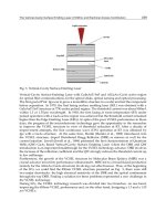
Fig 1. (left) open ended coaxial probe, (right) short ended coaxial probe test fixture
Open-ended coaxial test fixtures (OCP) (Fig 1-left) are the most popular techniques for
measuring of complex dielectric permittivity of many materials. Non-destructive,
broadband (RF and microwave ranges), and high-temperature (<= 1200 C) measurements
can be preformed with this method using commercially available instrumentation. The
measurements are performed by contacting one flat surface of the specimen or by
immersing the probe in the liquid sample. These techniques (Baker-Jarvis & Janezic, 1994;
chen et al. 1994) has been widely used due to the convenience of using one port
measurements to extract dielectric parameters and the relatively simple setup. Furthermore,
minimal sample preparation is required compared to other techniques, such as the
waveguide technique which will be seen later and which requires precisely machined bulk
samples and is generally classified as a destructive testing method.
There are two basic approaches to the determination of complex permittivity from the
measurements of the coaxial line open-circuit reflection coefficient; a rigorous solution
(Baker-Jarvis & Janezic, 1994; chen et al. 1994) of the electromagnetic field equations, and the
lumped equivalent approach utilising an admittance circuit to represent the probe fringing
fields. Nevertheless, theoretical formulations for the open-ended coaxial probe assume that
the MUT extends to infinity in the longitudinal and transverse directions, which is practical
when considering finite thin samples.
(chen et al. 1994) presented a method using an open coaxial probe where the material to be
measured (MUT) is backed by an arbitrary medium of semi-infinite thickness in a bi-layer
configuration (Fig 1-a). The coaxial line is considered to have an infinite flange extending in
MicrowaveandMillimeterWaveTechnologies:
fromPhotonicBandgapDevicestoAntennaandApplications292
the radial direction, while the MUT is considered to be linear, isotropic, homogeneous and
nonmagnetic in nature. It is further assumed that only TEM mode fields exist at the probe
aperture. The total terminal capacitance C
T
can be represented by:
T f 01 02
C =C +C +C
(1)
Where C
f
is the capacitance inside a Teflon-filled coaxial line while C
01
represents the
capacitance due to the fringing field outside the coaxial line into the finite sample and C
02
represents the capacitance of the fringing field into the infinitely thick medium that is used
to back the sample.
The final expression for the permittivity of the MUT after incorporating the error network is
expressed as:
1 2 2 2
1
3 2
g
(f,x,D, )
g
(f,x,D, )
a b
c 1 g (f,x,D, ) 1
(2)
Where ε
1
and ε
2
are the dielectric constants of the MUT and the infinite medium (dielectric
backing), respectively, x is the thickness of the MUT and D represents an empirical
parameter with dimensions of length, ρ is the measured reflection coefficient, a, b and c are
complex coefficients that are functions of frequency f. corresponding to functions g1, g2 and
g3 respectively which are, in turn, dependent on parameters f, x, D and ε
2
. To extract ε1,
three simultaneous equations are required to determine a, b and c, which are obtained by
measuring the reflection coefficients of three materials with known dielectric properties. The
model is valid at frequencies for which the line dimensions are small compared to the
wavelength.
The OCP method is very well suited for liquids or soft solid samples. It is accurate, fast, and
broadband (from 0.2 to up to 20 GHz). The measurement requires little sample preparation.
A major disadvantage of this method is that it is not suitable for measuring materials with
low dielectric property (plastics, oils, etc.) nor for thin films.
Short-circuited reflection: In these methods, a piece of sample is inserted in a segment of
shorted transmission line. An interesting method is presented by (Obrzut & Nozaki, 2001)
(Fig 1-right). A dielectric circular film (disk) specimen of thickness
t is placed at the end of
the center conductor of a coaxial airline. The diameter of the specimen ‘a’ matches that of the
central conductor and forms a circular parallel-plate capacitor terminating the coaxial line.
The incoming transverse-electromagnetic (TEM) wave approaches the sample section
through the coaxial line. The lumped capacitance model applies to this structure at higher
frequencies and still satisfies the quasi-static conditions as long as the length of the
propagating wave is much larger than the film thickness. The structure is electrically
equivalent to a network in which the dielectric film can be viewed as a transmission line
inserted between 2 matched transmission lines. The permittivity of the sample material is
written as follows:
s
11 f
*
p p
11
G
1 S C
j C C
1 S
(3)
where Gs is the conductance, Cp is the capacitance of the sample, C
f
is the fringing
capacitor, S11 is the reflection coefficient resulting from wave multiple reflection +
transmission components in the specimen section.
Short-terminated probes are better suited for thin film specimens. Dielectric materials of
precisely known permittivity are often used as a reference for correcting systematic errors
due to differences between the measurement and the calibration configurations. The
properties of the sample are derived from the reflection due to the impedance discontinuity
caused by the sample loading.
(b) Free space
Among the measurement techniques available, the techniques in free space (Varadan et al. 2000;
Lamkaouchi et al., 2003) belong to the nondestructive and contactless methods of measurement.
They consequently do not need special preparation of the sample; they can be used to measure
samples under special conditions, such as high temperature and particularly appropriate to the
measurement of non-homogeneous dielectric materials.
With such methods, a sample is placed between 2 antennas: a transmission antenna and a
reception antenna placed facing each other and connected to a network analyzer.
Fig. 2. Free space measurement bench with the sample placed between 2 antennas
Before starting the measurement, the VNA must first be calibrated. Then, using the de-
embedding function of the VNA, the influence of the sample holder can be cancelled out
and only the s-parameter of the MUT can be determined. Time domain gating should also
be applied to ensure there are no multiple reflections in the sample itself, though
appropriate thickness should able to avoid this. It also eliminates the diffraction of energy
from the edge of the antennas. Many conditions s are requirement to obtain perfect results:
- Far field requirements: to ensure that the wave incident to the sample from the antenna
can be taken as a plane wave, the distance d between the antenna and the sample should satisfy
the following far-field requirement: d > 2D
2
/λ, where λ is the wavelength of the operating
electromagnetic wave and D is the largest dimension of the antenna aperture. For an antenna
with circular aperture, D is the diameter of the aperture, and for an antenna with rectangular
aperture, D is the diagonal length of the rectangular aperture.
- Sample size: if the sample size is much smaller than the wavelength, the responses of
the sample to electromagnetic waves are similar to those of a particle object. To achieve
convincing results, the size of the sample should be larger than the wavelength of the
electromagnetic wave.
- Measurement environment: An anechoic room is preferable; we can also use time-
domain gating to eliminate the unwanted signal caused by environment reflections and multi-
reflections.
Characterizationtechniquesformaterials’propertiesmeasurement 293
the radial direction, while the MUT is considered to be linear, isotropic, homogeneous and
nonmagnetic in nature. It is further assumed that only TEM mode fields exist at the probe
aperture. The total terminal capacitance C
T
can be represented by:
T f 01 02
C =C +C +C
(1)
Where C
f
is the capacitance inside a Teflon-filled coaxial line while C
01
represents the
capacitance due to the fringing field outside the coaxial line into the finite sample and C
02
represents the capacitance of the fringing field into the infinitely thick medium that is used
to back the sample.
The final expression for the permittivity of the MUT after incorporating the error network is
expressed as:
1 2 2 2
1
3 2
g
(f,x,D, )
g
(f,x,D, )
a b
c 1 g (f,x,D, ) 1
(2)
Where ε
1
and ε
2
are the dielectric constants of the MUT and the infinite medium (dielectric
backing), respectively, x is the thickness of the MUT and D represents an empirical
parameter with dimensions of length, ρ is the measured reflection coefficient, a, b and c are
complex coefficients that are functions of frequency f. corresponding to functions g1, g2 and
g3 respectively which are, in turn, dependent on parameters f, x, D and ε
2
. To extract ε1,
three simultaneous equations are required to determine a, b and c, which are obtained by
measuring the reflection coefficients of three materials with known dielectric properties. The
model is valid at frequencies for which the line dimensions are small compared to the
wavelength.
The OCP method is very well suited for liquids or soft solid samples. It is accurate, fast, and
broadband (from 0.2 to up to 20 GHz). The measurement requires little sample preparation.
A major disadvantage of this method is that it is not suitable for measuring materials with
low dielectric property (plastics, oils, etc.) nor for thin films.
Short-circuited reflection: In these methods, a piece of sample is inserted in a segment of
shorted transmission line. An interesting method is presented by (Obrzut & Nozaki, 2001)
(Fig 1-right). A dielectric circular film (disk) specimen of thickness
t is placed at the end of
the center conductor of a coaxial airline. The diameter of the specimen ‘a’ matches that of the
central conductor and forms a circular parallel-plate capacitor terminating the coaxial line.
The incoming transverse-electromagnetic (TEM) wave approaches the sample section
through the coaxial line. The lumped capacitance model applies to this structure at higher
frequencies and still satisfies the quasi-static conditions as long as the length of the
propagating wave is much larger than the film thickness. The structure is electrically
equivalent to a network in which the dielectric film can be viewed as a transmission line
inserted between 2 matched transmission lines. The permittivity of the sample material is
written as follows:
s
11 f
*
p p
11
G
1 S C
j C C
1 S
(3)
where Gs is the conductance, Cp is the capacitance of the sample, C
f
is the fringing
capacitor, S11 is the reflection coefficient resulting from wave multiple reflection +
transmission components in the specimen section.
Short-terminated probes are better suited for thin film specimens. Dielectric materials of
precisely known permittivity are often used as a reference for correcting systematic errors
due to differences between the measurement and the calibration configurations. The
properties of the sample are derived from the reflection due to the impedance discontinuity
caused by the sample loading.
(b) Free space
Among the measurement techniques available, the techniques in free space (Varadan et al. 2000;
Lamkaouchi et al., 2003) belong to the nondestructive and contactless methods of measurement.
They consequently do not need special preparation of the sample; they can be used to measure
samples under special conditions, such as high temperature and particularly appropriate to the
measurement of non-homogeneous dielectric materials.
With such methods, a sample is placed between 2 antennas: a transmission antenna and a
reception antenna placed facing each other and connected to a network analyzer.
Fig. 2. Free space measurement bench with the sample placed between 2 antennas
Before starting the measurement, the VNA must first be calibrated. Then, using the de-
embedding function of the VNA, the influence of the sample holder can be cancelled out
and only the s-parameter of the MUT can be determined. Time domain gating should also
be applied to ensure there are no multiple reflections in the sample itself, though
appropriate thickness should able to avoid this. It also eliminates the diffraction of energy
from the edge of the antennas. Many conditions s are requirement to obtain perfect results:
- Far field requirements: to ensure that the wave incident to the sample from the antenna
can be taken as a plane wave, the distance d between the antenna and the sample should satisfy
the following far-field requirement: d > 2D
2
/λ, where λ is the wavelength of the operating
electromagnetic wave and D is the largest dimension of the antenna aperture. For an antenna
with circular aperture, D is the diameter of the aperture, and for an antenna with rectangular
aperture, D is the diagonal length of the rectangular aperture.
- Sample size: if the sample size is much smaller than the wavelength, the responses of
the sample to electromagnetic waves are similar to those of a particle object. To achieve
convincing results, the size of the sample should be larger than the wavelength of the
electromagnetic wave.
- Measurement environment: An anechoic room is preferable; we can also use time-
domain gating to eliminate the unwanted signal caused by environment reflections and multi-
reflections.
MicrowaveandMillimeterWaveTechnologies:
fromPhotonicBandgapDevicestoAntennaandApplications294
After that, from a precise phase measurement, a precise measurement of the permittivity on a
broad frequency band can thus be carried out using generally the “Nicolson–Ross–Weir
(NRW) algorithm” (Nicolson & Ross, 1970; Weir, 1974) where the reflection and
transmission are expressed by the scattering parameters S11 and S21 and explicit formulas
for the calculation of permittivity and permeability are derived.
2.2 Thin films measurements
(a) Short frequency band methods
Capacitive methods:
The basic methods for measuring the electromagnetic properties of materials at low
frequencies consists of placing the material in a measuring cell (capacitor, inductance) where
we measure the impedance Z or the admittance Y=1/Z (Mathai et al, 2002). The permittivity
of the material is deduced from the measured value of Z or Y using a localized elements
equivalent circuit representing the measurement cell. Capacitance techniques (Fig.
3)
include sandwiching the thin layer between two electrodes to form a capacitor. They are
useful at frequencies extending from fractions of a hertz to megahertz frequencies. Yet, with
very small conductors, specimens can be measured up to gigahertz frequencies (Park et al.
2005; Obrzut & Nozaki, 2001). Capacitance models work well if the wavelength is much
longer than the conductor separation. The capacitance for a parallel plate with no fringing
fields near the edges and the conductance (represent losses) at low frequency are written as:
A A
C and G
d d
"
(4)
The permittivity can be obtained from measurements of
C and G and is given by:
C-jG ω
ε =
r
C -jG ω
air air
(5)
This model assumes no fringing fields. A more accurate model would include the effects of
fringing fields. The use of guard electrodes as shown in Fig.
3 minimizes the effects of the
fringe field.
Fig. 3. A specimen in a capacitor with electrode guards.
Many procedures of measurement depending on the capacitive techniques have been
widely reported during the last decade. These methods whether using transmission lines,
interdigital capacitors or the classic capacitor, have their principle basics on measuring the
equivalent total impedance of the cell using an impedance analyser where we can measure
directly the capacitance and conductance or using a network analyser thus measuring the
reflection coefficient S11 and deducing the impedance of the whole structure using the
formula:
in 0 11 11
Z Z (1 S ) (1 S )
(6)
Then with an analytical work we go up with the dielectric permittivity of the material under
test. Other methods use very complicated equivalent circuit to represent the measurement
device and increase the accuracy of calculations.
Resonant cavities:
Resonant measurements are the most accurate methods of obtaining permittivity and
permeability. They are widely utilized because of its simplicity, easy data processing,
accuracy, and high temperature capabilities. There are many types of resonant techniques
available such as reentrant cavities, split cylinder resonators, cavity resonators, fabry-perot
resonators etc. This section will concentrate on the general overview of resonant
measurements and the general procedure using a cavity resonator.
The most popular resonant cavity method is the perturbation method (PM) (Komarov &
Yakovlev, 2003; Mathew & Raveendranath, 2001); it is designed in the standard TM
(transverse magnetic) or TE (transverse electric) mode of propagation of the electro-
magnetic fields. It is particularly suited for medium-loss and low-loss materials and
substances. Precisely shaped small-sized samples are usually used with this technique. But
PM provides dielectric properties measurements only at a resonant frequency, indicated by a
sharp increase in the magnitude of the |S
21
| parameter. The measurement is based on the
shift in resonant frequency and the change in absorption characteristics of a tuned resonant
cavity, due to insertion of a sample of target material (Janezic, 2004; Coakley et al. 2003). The
specimen is inserted through a clearance hole made at the center of the cavity and that’s into
region of maximum electric field.
Fig. 4. Resonant cavity with a bar sample inserted at its center.
Fig. 5. The resonance response with and without the sample.
Characterizationtechniquesformaterials’propertiesmeasurement 295
After that, from a precise phase measurement, a precise measurement of the permittivity on a
broad frequency band can thus be carried out using generally the “Nicolson–Ross–Weir
(NRW) algorithm” (Nicolson & Ross, 1970; Weir, 1974) where the reflection and
transmission are expressed by the scattering parameters S11 and S21 and explicit formulas
for the calculation of permittivity and permeability are derived.
2.2 Thin films measurements
(a) Short frequency band methods
Capacitive methods:
The basic methods for measuring the electromagnetic properties of materials at low
frequencies consists of placing the material in a measuring cell (capacitor, inductance) where
we measure the impedance Z or the admittance Y=1/Z (Mathai et al, 2002). The permittivity
of the material is deduced from the measured value of Z or Y using a localized elements
equivalent circuit representing the measurement cell. Capacitance techniques (Fig.
3)
include sandwiching the thin layer between two electrodes to form a capacitor. They are
useful at frequencies extending from fractions of a hertz to megahertz frequencies. Yet, with
very small conductors, specimens can be measured up to gigahertz frequencies (Park et al.
2005; Obrzut & Nozaki, 2001). Capacitance models work well if the wavelength is much
longer than the conductor separation. The capacitance for a parallel plate with no fringing
fields near the edges and the conductance (represent losses) at low frequency are written as:
A A
C and G
d d
"
(4)
The permittivity can be obtained from measurements of
C and G and is given by:
C-jG ω
ε =
r
C -jG ω
air air
(5)
This model assumes no fringing fields. A more accurate model would include the effects of
fringing fields. The use of guard electrodes as shown in Fig.
3 minimizes the effects of the
fringe field.
Fig. 3. A specimen in a capacitor with electrode guards.
Many procedures of measurement depending on the capacitive techniques have been
widely reported during the last decade. These methods whether using transmission lines,
interdigital capacitors or the classic capacitor, have their principle basics on measuring the
equivalent total impedance of the cell using an impedance analyser where we can measure
directly the capacitance and conductance or using a network analyser thus measuring the
reflection coefficient S11 and deducing the impedance of the whole structure using the
formula:
in 0 11 11
Z Z (1 S ) (1 S )
(6)
Then with an analytical work we go up with the dielectric permittivity of the material under
test. Other methods use very complicated equivalent circuit to represent the measurement
device and increase the accuracy of calculations.
Resonant cavities:
Resonant measurements are the most accurate methods of obtaining permittivity and
permeability. They are widely utilized because of its simplicity, easy data processing,
accuracy, and high temperature capabilities. There are many types of resonant techniques
available such as reentrant cavities, split cylinder resonators, cavity resonators, fabry-perot
resonators etc. This section will concentrate on the general overview of resonant
measurements and the general procedure using a cavity resonator.
The most popular resonant cavity method is the perturbation method (PM) (Komarov &
Yakovlev, 2003; Mathew & Raveendranath, 2001); it is designed in the standard TM
(transverse magnetic) or TE (transverse electric) mode of propagation of the electro-
magnetic fields. It is particularly suited for medium-loss and low-loss materials and
substances. Precisely shaped small-sized samples are usually used with this technique. But
PM provides dielectric properties measurements only at a resonant frequency, indicated by a
sharp increase in the magnitude of the |S
21
| parameter. The measurement is based on the
shift in resonant frequency and the change in absorption characteristics of a tuned resonant
cavity, due to insertion of a sample of target material (Janezic, 2004; Coakley et al. 2003). The
specimen is inserted through a clearance hole made at the center of the cavity and that’s into
region of maximum electric field.
Fig. 4. Resonant cavity with a bar sample inserted at its center.
Fig. 5. The resonance response with and without the sample.
MicrowaveandMillimeterWaveTechnologies:
fromPhotonicBandgapDevicestoAntennaandApplications296
When the dielectric specimen is inserted to the empty (air filled) cavity the resonant frequency
decreases from f
c
to f
s
while the bandwidth Δf at half power, i. e. 3 dB below the |S
21
| peak,
increases from Δf
c
to Δf
s
(see illustration in Fig. 5). A shift in resonant frequency is related to
the specimen dielectric constant, while the larger bandwidth corresponds to a smaller quality
factor Q (ratio of energy stored to energy dissipated), due to dielectric loss. The cavity
perturbation method involves measurements of f
c
, Δf
c
, f
s
, Δf
s
, and volume of the empty cavity
V
c
and the specimen volume V
s
. The quality factor for the empty cavity and for the cavity
filled with the specimen is given by the expressions:
c c c s s s
Q f / f , Q f / f
(7)
The real and imaginary parts of the dielectric constant are given by:
c c s c
' ''
r
s
r
s s s c
V f f V
1 1
1 ,
2V f 4V Q Q
(8)
As indicated before, this method requires that:
- The specimen volume be small compared to the volume of the whole cavity (V
s
<
0.1V
c
), which can lead to decreasing accuracy.
- The specimen must be positioned symmetrically in the region of maximum electric
field.
However, compared to other resonant test methods, the resonant cavity perturbation method
has several advantages such as overall good accuracy, simple calculations and test specimens
that are easy to shape.
(b) Large frequency band methods:
Wave guides:
Two types of hollow metallic waveguides are often used in microwave electronics:
rectangular waveguide and circular waveguide. Owing to the possible degenerations in
circular waveguides, rectangular waveguides are more widely used, while circular
waveguides have advantages in the characterization of chiral materials.
The waveguide usually works at TE10 mode. The width “a” and height “b” of a rectangular
waveguide satisfies b/a = ½. To ensure the single-mode requirement in materials property
characterization, the wavelength should be larger than “a” and less than “2a”, so that for a
given waveguide, there are limits for minimum frequency and maximum frequency. To
ensure good propagations, about 10% of the frequency range next to the minimum and
maximum frequency limits is not used. Several bands of waveguides often used in
microwave electronics and materials property characterization: X, Ka and Q bands.
The samples for rectangular waveguide method are relatively easy to fabricate, usually
rectangular substrates, and films deposited on such substrates.
(Quéffélec et al., 1999; 2000) presented a technique allowing broadband measurement of the
permeability tensor components together with the complex permittivity of ferrimagnetics
and/or of partly magnetized or saturated composite materials. It is based on the
measurement of the distribution parameters, S
ij
, of a rectangular waveguide whose section is
partly filled with the material under test (Fig.
6). The S
ij
-parameters are measured with a
vector network analyzer. The sample is rectangular and having the same width of the
waveguide, thus to eliminate any existence of air gap.
Fig. 6. Rectangular waveguide measurement cell, with a 2-layer sample fitting inside.
The determination of “ε” and “μ” of the material from the waveguide S
ij
requires to associate
an optimization program (inverse problem) to the dynamic electromagnetic analysis of the
cell (direct problem). The electromagnetic analysis of the cell is based on the mode-matching
method (Esteban & Rebollar, 1991) applied to the waveguide discontinuities. This method
requires the modes determination in the waveguide and the use of the orthogonality
conditions between the modes. The main problem in the modal analysis is the calculation of
the propagation constant for each mode in the waveguide partly filled with the material;
and then to match the modes in the plane of empty-cell/loaded-cell discontinuities. Such an
analysis allows a rigorous description of the dynamic behavior of the cell. The
electromagnetic analysis approach used is detailed in (Quéffélec et al., 1999).
The complex permittivity and complex components of the permeability tensor are computed
from a data-processing program, taking into account higher order modes excited at the cell
discontinuities and using a numerical optimization procedure (Quéffélec et al., 2000) to
match calculated and measured values of the S-parameters.
Lately the same procedure was used for the measurement of the permittivity of ferroelectric
thin film materials deposited on sapphire (Blasi & Queffelec, 2008) and good results were
obtained in the X-band. The goal is to have the less possible error E(x) for the equation
defined by:
2
th mes
ij ij
E x S x S x , where x ’, ’’ .
(9)
Where the indexes ‘th’ and ‘mes’ hold for the theoretical and measured parameters.
Transmission lines:
Transmission-line method (TLM) belongs to a large group of non-resonant methods of
measuring complex dielectric permittivity of different materials in a microwave range. They
involve placing the material inside a portion of an enclosed transmission line. The line is
usually a section of rectangular waveguide or coaxial airline. “εr” and “µr” are computed
from the measurement of the reflected signal (S
11
) and transmitted signal (S
21
). Free-space
technique, open-circuit network and the short-circuited network methods are included as a
part of this family. But, usually the main types of transmission lines used as the
Characterizationtechniquesformaterials’propertiesmeasurement 297
When the dielectric specimen is inserted to the empty (air filled) cavity the resonant frequency
decreases from f
c
to f
s
while the bandwidth Δf at half power, i. e. 3 dB below the |S
21
| peak,
increases from Δf
c
to Δf
s
(see illustration in Fig. 5). A shift in resonant frequency is related to
the specimen dielectric constant, while the larger bandwidth corresponds to a smaller quality
factor Q (ratio of energy stored to energy dissipated), due to dielectric loss. The cavity
perturbation method involves measurements of f
c
, Δf
c
, f
s
, Δf
s
, and volume of the empty cavity
V
c
and the specimen volume V
s
. The quality factor for the empty cavity and for the cavity
filled with the specimen is given by the expressions:
c c c s s s
Q f / f , Q f / f
(7)
The real and imaginary parts of the dielectric constant are given by:
c c s c
' ''
r
s
r
s s s c
V f f V
1 1
1 ,
2V f 4V Q Q
(8)
As indicated before, this method requires that:
- The specimen volume be small compared to the volume of the whole cavity (V
s
<
0.1V
c
), which can lead to decreasing accuracy.
- The specimen must be positioned symmetrically in the region of maximum electric
field.
However, compared to other resonant test methods, the resonant cavity perturbation method
has several advantages such as overall good accuracy, simple calculations and test specimens
that are easy to shape.
(b) Large frequency band methods:
Wave guides:
Two types of hollow metallic waveguides are often used in microwave electronics:
rectangular waveguide and circular waveguide. Owing to the possible degenerations in
circular waveguides, rectangular waveguides are more widely used, while circular
waveguides have advantages in the characterization of chiral materials.
The waveguide usually works at TE10 mode. The width “a” and height “b” of a rectangular
waveguide satisfies b/a = ½. To ensure the single-mode requirement in materials property
characterization, the wavelength should be larger than “a” and less than “2a”, so that for a
given waveguide, there are limits for minimum frequency and maximum frequency. To
ensure good propagations, about 10% of the frequency range next to the minimum and
maximum frequency limits is not used. Several bands of waveguides often used in
microwave electronics and materials property characterization: X, Ka and Q bands.
The samples for rectangular waveguide method are relatively easy to fabricate, usually
rectangular substrates, and films deposited on such substrates.
(Quéffélec et al., 1999; 2000) presented a technique allowing broadband measurement of the
permeability tensor components together with the complex permittivity of ferrimagnetics
and/or of partly magnetized or saturated composite materials. It is based on the
measurement of the distribution parameters, S
ij
, of a rectangular waveguide whose section is
partly filled with the material under test (Fig.
6). The S
ij
-parameters are measured with a
vector network analyzer. The sample is rectangular and having the same width of the
waveguide, thus to eliminate any existence of air gap.
Fig. 6. Rectangular waveguide measurement cell, with a 2-layer sample fitting inside.
The determination of “ε” and “μ” of the material from the waveguide S
ij
requires to associate
an optimization program (inverse problem) to the dynamic electromagnetic analysis of the
cell (direct problem). The electromagnetic analysis of the cell is based on the mode-matching
method (Esteban & Rebollar, 1991) applied to the waveguide discontinuities. This method
requires the modes determination in the waveguide and the use of the orthogonality
conditions between the modes. The main problem in the modal analysis is the calculation of
the propagation constant for each mode in the waveguide partly filled with the material;
and then to match the modes in the plane of empty-cell/loaded-cell discontinuities. Such an
analysis allows a rigorous description of the dynamic behavior of the cell. The
electromagnetic analysis approach used is detailed in (Quéffélec et al., 1999).
The complex permittivity and complex components of the permeability tensor are computed
from a data-processing program, taking into account higher order modes excited at the cell
discontinuities and using a numerical optimization procedure (Quéffélec et al., 2000) to
match calculated and measured values of the S-parameters.
Lately the same procedure was used for the measurement of the permittivity of ferroelectric
thin film materials deposited on sapphire (Blasi & Queffelec, 2008) and good results were
obtained in the X-band. The goal is to have the less possible error E(x) for the equation
defined by:
2
th mes
ij ij
E x S x S x , where x ’, ’’ .
(9)
Where the indexes ‘th’ and ‘mes’ hold for the theoretical and measured parameters.
Transmission lines:
Transmission-line method (TLM) belongs to a large group of non-resonant methods of
measuring complex dielectric permittivity of different materials in a microwave range. They
involve placing the material inside a portion of an enclosed transmission line. The line is
usually a section of rectangular waveguide or coaxial airline. “εr” and “µr” are computed
from the measurement of the reflected signal (S
11
) and transmitted signal (S
21
). Free-space
technique, open-circuit network and the short-circuited network methods are included as a
part of this family. But, usually the main types of transmission lines used as the
MicrowaveandMillimeterWaveTechnologies:
fromPhotonicBandgapDevicestoAntennaandApplications298
measurement cell in TLM are: coaxial line (Vanzura et al. 1994; Shenhui et al., 2003), strip
line (Salahun et al. 2001), and the planar circuits: micro-strip line (Queffellec & Gelin, 1994;
Janezic et al. 2003), slot line (planar capacitor) (Petrov et al. 2005), coplanar waveguide (Lue
& Tseng, 2001; Hinojosa et al., 2002) and inter-digital capacitors (Su et al., 2000; Al-Shareef
et al. 1997).
Coaxial line: Due to their relative simplicity, coaxial line transmission or reflection methods
are widely used broadband measurement techniques. In these methods, a precisely
machined specimen (Fig. 7
Error! Reference source not found.) is placed in a section of
coaxial line totally filling this section, and the scattering parameters are measured. The
relevant scattering equations relate the measured scattering parameters to the permittivity
and permeability of the material.
Fig. 7. Coaxial structure with the material to be tested filling completely a section part.
For TEM mode, the complex relative permeability and permittivity can be found as
(Shenhui et al., 2003):
r 0 s r s 0
Z jZ 2 , Z jZ 2
(10)
Where Zs is the characteristic impedance of the sample, Z0 is the characteristic impedance of
the air for the same dimensions, λ is the free space wavelength and γ is the propagation
constant written in terms of S-parameters as follows:
2 2
11 211
21
(1 S S )
l cosh
2S
(11)
And “l” is the sample thickness.
Corrections for the effects of air gaps between the specimen holder and the sample can be
made by analytical formulas (Vanzura et al., 1994). For coaxial lines, an annular sample
needs to be fabricated. The thickness of the sample should be approximately one-quarter of
the wavelength of the energy that has penetrated the sample. Although this method is more
accurate and sensitive than the more recent coaxial probe method, it has a narrower range of
frequencies. As the substance must fill the cross-section of the coaxial transmission line,
sample preparation is also more difficult and time consuming.
Strip line: This method (Salahun et al., 2001) allows a broad-band measurement of the
complex permittivity and permeability of solid and isotropic materials. The samples to be
tested are either rectangular plates or thin films put (or mounted) on a dielectric holder. This
method is based on the determination of the distribution parameters, S
ij
, of a 3-plate
transmission microstrip line that contains the material to be tested (Fig.
8).
Fig. 8. Strip line measuring cell: Schematic drawing of an asymmetrical stripline structure.
The sample is laid on the ground plane (Source: Salahun et al. 2001).
The method presents 3 steps: firstly, the theoretical effective permittivity and effective
permeability are calculated from:
th th
0 0
eff eff
ε =C C and µ =L L
(12)
Where (L,C) and (L
0
,C
0
) are the inductance and capacitance per unit of length calculated in
the cell with and without the sample. In the 2
nd
step, supposing a TEM mode in the cell, the
effective permittivity and permeability are calculated using the Nicolson/Ross procedure
mentioned in the free space method previously. In the last step, the complex electromagnetic
parameters of the material are calculated by matching theoretical and measured effective
values. Errors equations for the complex permeability and permittivity of the material are
solved using a dichotomous procedure in the complex plane.
th
m
2
eff eff
th
m
2
eff eff
F(µ',µ") |µ µ |
G( ', ") | |
(13)
The method enables one to get rid of sample machining problems (presented in the previous
coaxial line methods) since the latter does not fully fill in the cross-section of the cell.
Micro-strip line: Microstrips have long been used as microwave components, and show
many properties which overcome some of the limitations of non-planar components, thus
making it suitable for use in dielectric permittivity measurement. These methods can be
destructive and non-destructive. A destructive technique in presented by (Janezic et al.,
2003), where the thin film is incorporated in the microstrip line. The advantage of this
technique is the ability to separate the electrical properties of the metal conductors from the
electrical properties of the thin film by separate measurements of the propagation constant
and the characteristic impedance of the microstrip line. From the propagation constant and
characteristic impedance, the measured distributed capacitance and conductance of the
microstrip line are determined. Then knowing the physical dimensions of the microstrip
lines, the thin-film permittivity is related to the measured capacitance by using a finite-
difference solver. Yet precise, a more advantageous method is a non-destructive where the
material to be measured is left intact for later integration in applications. A method of this
type is published in the work of (Queffellec & Gelin, 1994) where the material to be
measured is placed on the microstrip line. And as, it is well known that the effective
permittivity (a combination of the substrate permittivity and the permittivity of the material
above the line) of a microstrip transmission line (at least for thin width-to-height ratios) is
Characterizationtechniquesformaterials’propertiesmeasurement 299
measurement cell in TLM are: coaxial line (Vanzura et al. 1994; Shenhui et al., 2003), strip
line (Salahun et al. 2001), and the planar circuits: micro-strip line (Queffellec & Gelin, 1994;
Janezic et al. 2003), slot line (planar capacitor) (Petrov et al. 2005), coplanar waveguide (Lue
& Tseng, 2001; Hinojosa et al., 2002) and inter-digital capacitors (Su et al., 2000; Al-Shareef
et al. 1997).
Coaxial line: Due to their relative simplicity, coaxial line transmission or reflection methods
are widely used broadband measurement techniques. In these methods, a precisely
machined specimen (Fig. 7
Error! Reference source not found.) is placed in a section of
coaxial line totally filling this section, and the scattering parameters are measured. The
relevant scattering equations relate the measured scattering parameters to the permittivity
and permeability of the material.
Fig. 7.
Coaxial structure with the material to be tested filling completely a section part.
For TEM mode, the complex relative permeability and permittivity can be found as
(Shenhui et al., 2003):
r 0 s r s 0
Z jZ 2 , Z jZ 2
(10)
Where Zs is the characteristic impedance of the sample, Z0 is the characteristic impedance of
the air for the same dimensions, λ is the free space wavelength and γ is the propagation
constant written in terms of S-parameters as follows:
2 2
11 211
21
(1 S S )
l cosh
2S
(11)
And “l” is the sample thickness.
Corrections for the effects of air gaps between the specimen holder and the sample can be
made by analytical formulas (Vanzura et al., 1994). For coaxial lines, an annular sample
needs to be fabricated. The thickness of the sample should be approximately one-quarter of
the wavelength of the energy that has penetrated the sample. Although this method is more
accurate and sensitive than the more recent coaxial probe method, it has a narrower range of
frequencies. As the substance must fill the cross-section of the coaxial transmission line,
sample preparation is also more difficult and time consuming.
Strip line: This method (Salahun et al., 2001) allows a broad-band measurement of the
complex permittivity and permeability of solid and isotropic materials. The samples to be
tested are either rectangular plates or thin films put (or mounted) on a dielectric holder. This
method is based on the determination of the distribution parameters, S
ij
, of a 3-plate
transmission microstrip line that contains the material to be tested (Fig.
8).
Fig. 8. Strip line measuring cell: Schematic drawing of an asymmetrical stripline structure.
The sample is laid on the ground plane (Source: Salahun et al. 2001).
The method presents 3 steps: firstly, the theoretical effective permittivity and effective
permeability are calculated from:
th th
0 0
eff eff
ε =C C and µ =L L
(12)
Where (L,C) and (L
0
,C
0
) are the inductance and capacitance per unit of length calculated in
the cell with and without the sample. In the 2
nd
step, supposing a TEM mode in the cell, the
effective permittivity and permeability are calculated using the Nicolson/Ross procedure
mentioned in the free space method previously. In the last step, the complex electromagnetic
parameters of the material are calculated by matching theoretical and measured effective
values. Errors equations for the complex permeability and permittivity of the material are
solved using a dichotomous procedure in the complex plane.
th
m
2
eff eff
th
m
2
eff eff
F(µ',µ") |µ µ |
G( ', ") | |
(13)
The method enables one to get rid of sample machining problems (presented in the previous
coaxial line methods) since the latter does not fully fill in the cross-section of the cell.
Micro-strip line: Microstrips have long been used as microwave components, and show
many properties which overcome some of the limitations of non-planar components, thus
making it suitable for use in dielectric permittivity measurement. These methods can be
destructive and non-destructive. A destructive technique in presented by (Janezic et al.,
2003), where the thin film is incorporated in the microstrip line. The advantage of this
technique is the ability to separate the electrical properties of the metal conductors from the
electrical properties of the thin film by separate measurements of the propagation constant
and the characteristic impedance of the microstrip line. From the propagation constant and
characteristic impedance, the measured distributed capacitance and conductance of the
microstrip line are determined. Then knowing the physical dimensions of the microstrip
lines, the thin-film permittivity is related to the measured capacitance by using a finite-
difference solver. Yet precise, a more advantageous method is a non-destructive where the
material to be measured is left intact for later integration in applications. A method of this
type is published in the work of (Queffellec & Gelin, 1994) where the material to be
measured is placed on the microstrip line. And as, it is well known that the effective
permittivity (a combination of the substrate permittivity and the permittivity of the material
above the line) of a microstrip transmission line (at least for thin width-to-height ratios) is
MicrowaveandMillimeterWaveTechnologies:
fromPhotonicBandgapDevicestoAntennaandApplications300
strongly dependent on the permittivity of the region above the line, this effect has been
utilized in implementing microwave circuits and to a lesser extent investigation of dielectric
permittivity.
Fig. 9. Microstrip device loaded with the sample (Source: Queffelec et al. 1998).
This method (Fig.
9) allows a broad-band measurement of the complex permittivity and
permeability of solid and isotropic materials. The samples to be tested are either rectangular
plates or thin films. This method is based on the determination of the distribution
parameters, S
ij
, of a microstrip line that contains the material to be tested. The method is
original because the sample is directly placed onto the line substrate without needing to
fully fill in the cross-section of the cell as in the case of waveguides and coaxial cables. The
analysis of measured data, that is, the determination of complex “ε” and “µ” from S
ij
requires associating an optimization program (inverse problem) to the electromagnetic
analysis of the cell (direct problem) as follows:
The spectral domain approach was used in the direct problem, allows one to take
into account several propagation modes in the calculation. and later in (Queffelec et al.,
1998) the mode matching method.
The inverse problem is solved using a numerical optimization process based on the
Raphson-Newton method and the results for the permittivity and permeability were
obtained on a large frequency band up to 18 GHz.
Slot line (Planar capacitor): One of the simplest devices for evaluating the electrical
properties of ferroelectric materials is the capacitor. There are two types: parallel plate
capacitors discussed above, where the ferroelectric layer is sandwiched between the
electrodes; and planar capacitors, where the electrodes are patterned on the same side of a
ferroelectric film and are separated by a small gap (Petrov et al., 2005).
Fig. 10. Planar capacitor structure and its equivalent circuit (Rs and Rp are the series and
parallel resistors representing loss).
Fig. 10 shows the planar capacitor device used for measurement of the dielectric
permittivity of the ferroelectric thin film incorporated in the structure (destructive) and its
equivalent circuit model used to go up with the total impedance of the structure through
measuring the reflection coefficient S11 and then the impedance using equation (6). And the
permittivity of the thin film is written as follows:
D D F
F D
0 F
1 h h
C 2 l s 4
ln 4 ln 16 ln(2)
w s s h
(14)
Where, C is the capacitance of the structure, h
F
is the ferroelectric lm thickness; h
D
is the
substrate thickness, s
is the gap width, l is the electrode length, w is the electrode width and ε
D
is the dielectric
constant of the substrate. It should be noted that equation (26) is valid under the following
limitations: ε
F
/ε
D
≥ 10
2
,
h
F
< s< 10h
F
, s< 0.25l and s< 0.5hD. Using this approach, the dielectric permittivity of the
STO lm was evaluated to be about ε’
3500 at 77 K, 6 GHz.
Coplanar lines: The coplanar lines were the subject of increasing interest during the last
decade in that they present a solution at the technical problems, encountered in the design
of the strip and micro-strip standard transmission lines (their adaptation to the external
circuits is easier and their use offers relatively low dispersion at high frequencies).
Many characterization methods using coplanar lines are published. (Hinojosa, et al. 2002)
presented an easy, fast, destructive and very high broadband (0.05–110 GHz)
electromagnetic characterization method using a coplanar line as a cell measurement to
measure the permittivity of a dielectric material on which the line is directly printed (Fig.
11). The direct problem consists of computing the S-parameters at the access planes of the
coplanar cell under test propagating only the quasi-TEM mode. The optimization procedure
(the inverse problem) is based on an iterative method derived from the gradient method
(Hinojosa et al., 2001), simultaneously carrying out the ‘ε
r
’ and ‘µ
r
’ computation and the
convergence between (S
11
, S
21
) measured values and those computed by the direct problem
through successive increment of the permittivity and permeability values.
Another method is presented by (Lue & Tseng, 2001). A technique using a coplanar
waveguide incorporating the ferroelectric thin film deposited on a dielectric substrate.
Fig. 11. Coplanar line incorporating the thin ferroelectric film.
It is based on an easy and fast processing method of the coplanar S-parameter
measurements, which takes into account the quasi-TEM mode propagation. Analytical
relationships compute the propagation constant and characteristic impedance of the
coplanar cell instead of any numerical method, which considerably decreases computation
time, and the effective permittivity of the multi-layered structure is deduced. The S-
Characterizationtechniquesformaterials’propertiesmeasurement 301
strongly dependent on the permittivity of the region above the line, this effect has been
utilized in implementing microwave circuits and to a lesser extent investigation of dielectric
permittivity.
Fig. 9. Microstrip device loaded with the sample (Source: Queffelec et al. 1998).
This method (Fig.
9) allows a broad-band measurement of the complex permittivity and
permeability of solid and isotropic materials. The samples to be tested are either rectangular
plates or thin films. This method is based on the determination of the distribution
parameters, S
ij
, of a microstrip line that contains the material to be tested. The method is
original because the sample is directly placed onto the line substrate without needing to
fully fill in the cross-section of the cell as in the case of waveguides and coaxial cables. The
analysis of measured data, that is, the determination of complex “ε” and “µ” from S
ij
requires associating an optimization program (inverse problem) to the electromagnetic
analysis of the cell (direct problem) as follows:
The spectral domain approach was used in the direct problem, allows one to take
into account several propagation modes in the calculation. and later in (Queffelec et al.,
1998) the mode matching method.
The inverse problem is solved using a numerical optimization process based on the
Raphson-Newton method and the results for the permittivity and permeability were
obtained on a large frequency band up to 18 GHz.
Slot line (Planar capacitor): One of the simplest devices for evaluating the electrical
properties of ferroelectric materials is the capacitor. There are two types: parallel plate
capacitors discussed above, where the ferroelectric layer is sandwiched between the
electrodes; and planar capacitors, where the electrodes are patterned on the same side of a
ferroelectric film and are separated by a small gap (Petrov et al., 2005).
Fig. 10. Planar capacitor structure and its equivalent circuit (Rs and Rp are the series and
parallel resistors representing loss).
Fig. 10 shows the planar capacitor device used for measurement of the dielectric
permittivity of the ferroelectric thin film incorporated in the structure (destructive) and its
equivalent circuit model used to go up with the total impedance of the structure through
measuring the reflection coefficient S11 and then the impedance using equation (6). And the
permittivity of the thin film is written as follows:
D D F
F D
0 F
1 h h
C 2 l s 4
ln 4 ln 16 ln(2)
w s s h
(14)
Where, C is the capacitance of the structure, h
F
is the ferroelectric lm thickness; h
D
is the
substrate thickness, s
is the gap width, l is the electrode length, w is the electrode width and ε
D
is the dielectric
constant of the substrate. It should be noted that equation (26) is valid under the following
limitations: ε
F
/ε
D
≥ 10
2
,
h
F
< s< 10h
F
, s< 0.25l and s< 0.5hD. Using this approach, the dielectric permittivity of the
STO lm was evaluated to be about ε’
3500 at 77 K, 6 GHz.
Coplanar lines: The coplanar lines were the subject of increasing interest during the last
decade in that they present a solution at the technical problems, encountered in the design
of the strip and micro-strip standard transmission lines (their adaptation to the external
circuits is easier and their use offers relatively low dispersion at high frequencies).
Many characterization methods using coplanar lines are published. (Hinojosa, et al. 2002)
presented an easy, fast, destructive and very high broadband (0.05–110 GHz)
electromagnetic characterization method using a coplanar line as a cell measurement to
measure the permittivity of a dielectric material on which the line is directly printed (Fig.
11). The direct problem consists of computing the S-parameters at the access planes of the
coplanar cell under test propagating only the quasi-TEM mode. The optimization procedure
(the inverse problem) is based on an iterative method derived from the gradient method
(Hinojosa et al., 2001), simultaneously carrying out the ‘ε
r
’ and ‘µ
r
’ computation and the
convergence between (S
11
, S
21
) measured values and those computed by the direct problem
through successive increment of the permittivity and permeability values.
Another method is presented by (Lue & Tseng, 2001). A technique using a coplanar
waveguide incorporating the ferroelectric thin film deposited on a dielectric substrate.
Fig. 11. Coplanar line incorporating the thin ferroelectric film.
It is based on an easy and fast processing method of the coplanar S-parameter
measurements, which takes into account the quasi-TEM mode propagation. Analytical
relationships compute the propagation constant and characteristic impedance of the
coplanar cell instead of any numerical method, which considerably decreases computation
time, and the effective permittivity of the multi-layered structure is deduced. The S-
MicrowaveandMillimeterWaveTechnologies:
fromPhotonicBandgapDevicestoAntennaandApplications302
parameter measurement bench of the coplanar cells employs vector network analyzers and
commercially available high-quality on-coplanar test fixtures (probe station). The extraction
of the permittivity of the thin film is done using the conformal mapping analysis.
Coplanar interdigital capacitor:
Another type of characterization methods which use the coplanar wave guide structure are
those of the coplanar interdigital capacitor. These methods have the strip line or the central
conductor in the form of interdigitated fingers (Fig.
12) in a way to increase the
electromagnetic interaction between the propagating wave and the sample, thus increasing
the sensitivity of the structure.
Fig. 12. coplanar IDC (left) with fingers parallel to the wave propagation with a schematic of
a cross section of the capacitor structure (right).
As reported by (Al-Shareef et al., 1997); to calculate the dielectric constant of the thin film
capacitors with the interdigital electrode configuration shown in Fig.
12, an analytical
model previously derived by Farnell et al. was employed (Farnell et al., 1970). Based on
Farnell's analysis, it can be shown that the dielectric constant of a thin film having the
configuration shown in Fig. 1 can be calculated using the following expression:
f s s
-4.6h
= + C-K 1+ K 1-exp
L
(15)
where ef and es are the film and substrate dielectric constants, respectively; h is the film
thickness, K is a constant which has units of pF, and C is the measured capacitance per unit
finger length per electrode section of width L (L is half the IDE pattern period or l=2).
Another procedure for low frequency measurement is to measure directly the impedance
using an impedance analyzer (1 layer material case), or using the conformal mapping
method to calculate analytically, the capacitance of the structure and compare this latter to
the measured value thus deducing the permittivity of the material under test.
3. Non-destructive transmission line method: Characterization using a
Coplanar line
Principles and techniques of permittivity measurements using transmission lines have been
illustrated in the preceding part. Yet, most of these methods have the thin film incorporated
inside the device (Lue & Tseng, 2001) (a destructive method), which prevent using the
measured film material in an electronic circuit. And as ferroelectric film deposition and
permittivity values still not well controlled, this poses a problem in their integration.
Therefore, a non-destructive method will be the most appropriate for such situation as well
as for industrial use in general.
We present here a nouvelle and non-destructive Broadband characterization method which
employs a coplanar line for the measurement of the complex permittivity of linear dielectric
materials and precisely, that of ferroelectric thin films. The method uses the transmission
coefficient supposing a quasi-TEM analysis to find the effective permittivity of the
multilayer system. In the inverse problem, the coplanar conformal mapping technique is
employed to extract the relative permittivity of the thin layer.
3.1 Theory and analysis
The theory of the method and its principle is very simple; the substrate to be measured is
placed on the line for an assembly as described in Fig.
13 below, where the line is taken in
sandwich between 2 dielectric substrates, that of the line and the material to measure.
Fig. 13. Schematic of a CPW tight between two dielectrics: Alumina substrate from below
and the ferroelectric thin film + MgO substrate from above.
The method includes measuring ‘only’ the transmission coefficient S
21
of the device and
that’s in two steps: - the first for the coplanar line in air (without material), - and the other
with the line loaded with material whether of one layer or multi-layers.
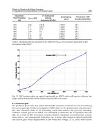
The effects of the different materials on the dispersion parameters of the line results of these
measurements are presented in Fig.
14.
0 5 10 15 20
-2,8
-2,4
-2,0
-1,6
-1,2
-0,8
-0,4
0,0
unloaded
loaded with MgO
loaded with Ferroelectric device
S21 (dB)
Frequency (GHz)
Fig. 14. S-parameters measured with 3 different samples placed on the coplanar line:
unloaded (air), MgO substrate and 2-layered device: MgO + ferroelectric thin film
Characterizationtechniquesformaterials’propertiesmeasurement 303
parameter measurement bench of the coplanar cells employs vector network analyzers and
commercially available high-quality on-coplanar test fixtures (probe station). The extraction
of the permittivity of the thin film is done using the conformal mapping analysis.
Coplanar interdigital capacitor:
Another type of characterization methods which use the coplanar wave guide structure are
those of the coplanar interdigital capacitor. These methods have the strip line or the central
conductor in the form of interdigitated fingers (Fig.
12) in a way to increase the
electromagnetic interaction between the propagating wave and the sample, thus increasing
the sensitivity of the structure.
Fig. 12. coplanar IDC (left) with fingers parallel to the wave propagation with a schematic of
a cross section of the capacitor structure (right).
As reported by (Al-Shareef et al., 1997); to calculate the dielectric constant of the thin film
capacitors with the interdigital electrode configuration shown in Fig.
12, an analytical
model previously derived by Farnell et al. was employed (Farnell et al., 1970). Based on
Farnell's analysis, it can be shown that the dielectric constant of a thin film having the
configuration shown in Fig. 1 can be calculated using the following expression:
f s s
-4.6h
= + C-K 1+ K 1-exp
L
(15)
where ef and es are the film and substrate dielectric constants, respectively; h is the film
thickness, K is a constant which has units of pF, and C is the measured capacitance per unit
finger length per electrode section of width L (L is half the IDE pattern period or l=2).
Another procedure for low frequency measurement is to measure directly the impedance
using an impedance analyzer (1 layer material case), or using the conformal mapping
method to calculate analytically, the capacitance of the structure and compare this latter to
the measured value thus deducing the permittivity of the material under test.
3. Non-destructive transmission line method: Characterization using a
Coplanar line
Principles and techniques of permittivity measurements using transmission lines have been
illustrated in the preceding part. Yet, most of these methods have the thin film incorporated
inside the device (Lue & Tseng, 2001) (a destructive method), which prevent using the
measured film material in an electronic circuit. And as ferroelectric film deposition and
permittivity values still not well controlled, this poses a problem in their integration.
Therefore, a non-destructive method will be the most appropriate for such situation as well
as for industrial use in general.
We present here a nouvelle and non-destructive Broadband characterization method which
employs a coplanar line for the measurement of the complex permittivity of linear dielectric
materials and precisely, that of ferroelectric thin films. The method uses the transmission
coefficient supposing a quasi-TEM analysis to find the effective permittivity of the
multilayer system. In the inverse problem, the coplanar conformal mapping technique is
employed to extract the relative permittivity of the thin layer.
3.1 Theory and analysis
The theory of the method and its principle is very simple; the substrate to be measured is
placed on the line for an assembly as described in Fig.
13 below, where the line is taken in
sandwich between 2 dielectric substrates, that of the line and the material to measure.
Fig. 13. Schematic of a CPW tight between two dielectrics: Alumina substrate from below
and the ferroelectric thin film + MgO substrate from above.
The method includes measuring ‘only’ the transmission coefficient S
21
of the device and
that’s in two steps: - the first for the coplanar line in air (without material), - and the other
with the line loaded with material whether of one layer or multi-layers.
The effects of the different materials on the dispersion parameters of the line results of these
measurements are presented in Fig.
14.
0 5 10 15 20
-2,8
-2,4
-2,0
-1,6
-1,2
-0,8
-0,4
0,0
unloaded
loaded with MgO
loaded with Ferroelectric device
S21 (dB)
Frequency (GHz)
Fig. 14. S-parameters measured with 3 different samples placed on the coplanar line:
unloaded (air), MgO substrate and 2-layered device: MgO + ferroelectric thin film
MicrowaveandMillimeterWaveTechnologies:
fromPhotonicBandgapDevicestoAntennaandApplications304
The measurement procedure is presented in 2 problems: a direct one and an inverse one.
3.2 Analysis of the direct problem
The analysis is based on the measurements of the S-parameters of the line and precisely the
transmission coefficient S
21
. We have for a standard transmission line the S-parameters
written as follows:
ij
0 e
S
e 0
(16)
Where L is the line length, and
l
is the S
21
phase shift. The propagation constant of a
coplanar wave guide is well known to be:
eff eff
2
j f
c
(17)
The ratio of the two measurements mentioned gives the following formula:
v c
reff reff
c v
(loaded)
21 21
(unloaded)
2
j
.f.l.( )
( )
c
S S
e e
(18)
Where (γ
c
) and (γ
v
) are propagation constant of the system with and without the load
respectively, ε
eff
is the effective permittivity of the whole system, µ
eff
the effective
permeability which is equal to ‘1’ in the case of dielectric medium and ‘ƒ’ is the frequency.
This equation makes it possible to extract the effective permittivity of the complete system
(line + DUT) that we will note “ε
effc
”.
3.3 Quasi-TEM analysis and Inverse problem
From the previous analysis, we extracted the effective permittivity of the complete system
(coplanar line+ coplanar substrate + the material to be measured (1-layer or 2-layers)). In
this section, the conformal mapping analysis is carried out to solve the inverse problem. The
conformal mapping technique assumes a quasi-static TEM mode of propagation along the
line. Closed form expressions for the effective permittivity and the characteristic impedance
for CPW are presented in (Simons, 2001). The simplified formulas for the sandwiched 3-
layered CPW structure are given here; where we have the effective permittivity written as
follows:
eff 1 r1 2 r2 3 r3 r2
1 q 1 q 1 q
(19)
With εr1 is the dielectric constant of the line substrate, εr2 is that of the thin film substrate
(the substrate on which the film is deposited), εr3 is the permittivity of the thin film and qi is
the partial filling factor equal to:
0
i
i
i 0
K' k
K k
1
q ,i 1,2,3,
2 K' k K k
(20)
K(x) is the complete elliptical integral of first kind, and
2
K'(x)=K( 1 x )
and their modulus
k
0
and k
i
are written:
0 i
i i
s 2w
s
k s (s 2w),k sinh sinh
4h 4h
(21)
s and w are the CPW conductor and slot width respectively, h
i
is the thickness of the 3
different layers.
To simplify our calculations usually we employ the asymptotic formula for the ratio of
elliptic function and that under the following conditions:
For
i
i
i i i
i
2 1 J
K k
0 k 0.707 ln where J 1 k
K' ki
1 J
(22)
and for
i
i
i
i
i
2 1 k
K k
k 0.707 ln
K' k
1 k
(23)
For a thickness h
i
too small compared to the line parameters, that is, if s, w >> h
3
(which is
the case)
,
k
3
become too small (k
3
<<<1), which leads to a numerical error in calculating the
elliptic function. To overcome this difficulty, for the special case (Zhao, 2005) when
k
i
≈0;
i
i
2
i
i
i
1 1 k
K k
16
ln 2 ln
k
K' k
1 1 k
(24)
The resolution of the inverse problem is carried out by applying these formulas which
makes it possible to determine the permittivity of material. In the quasi-TEM case, these
simplified expressions for a tri-layer structure make it possible to extract the complex
permittivity of the thin layer ‘ε
r3
’ from the following equation:
eff 1 r1 2 r2
r3 r2
3
1 q 1 q 1
q
(25)
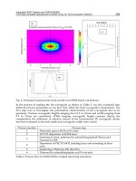
3.4 Numerical Calculation (FEM, TLM)
An analysis based on the conformal mapping method was done using a Matlab program.
With this program we studied the effect of the material placed on the line on the effective
permittivity of the system (Figure 15):
Characterizationtechniquesformaterials’propertiesmeasurement 305
The measurement procedure is presented in 2 problems: a direct one and an inverse one.
3.2 Analysis of the direct problem
The analysis is based on the measurements of the S-parameters of the line and precisely the
transmission coefficient S
21
. We have for a standard transmission line the S-parameters
written as follows:
ij
0 e
S
e 0
(16)
Where L is the line length, and
l
is the S
21
phase shift. The propagation constant of a
coplanar wave guide is well known to be:
eff eff
2
j f
c
(17)
The ratio of the two measurements mentioned gives the following formula:
v c
reff reff
c v
(loaded)
21 21
(unloaded)
2
j
.f.l.( )
( )
c
S S
e e
(18)
Where (γ
c
) and (γ
v
) are propagation constant of the system with and without the load
respectively, ε
eff
is the effective permittivity of the whole system, µ
eff
the effective
permeability which is equal to ‘1’ in the case of dielectric medium and ‘ƒ’ is the frequency.
This equation makes it possible to extract the effective permittivity of the complete system
(line + DUT) that we will note “ε
effc
”.
3.3 Quasi-TEM analysis and Inverse problem
From the previous analysis, we extracted the effective permittivity of the complete system
(coplanar line+ coplanar substrate + the material to be measured (1-layer or 2-layers)). In
this section, the conformal mapping analysis is carried out to solve the inverse problem. The
conformal mapping technique assumes a quasi-static TEM mode of propagation along the
line. Closed form expressions for the effective permittivity and the characteristic impedance
for CPW are presented in (Simons, 2001). The simplified formulas for the sandwiched 3-
layered CPW structure are given here; where we have the effective permittivity written as
follows:
eff 1 r1 2 r2 3 r3 r2
1 q 1 q 1 q
(19)
With εr1 is the dielectric constant of the line substrate, εr2 is that of the thin film substrate
(the substrate on which the film is deposited), εr3 is the permittivity of the thin film and qi is
the partial filling factor equal to:
0
i
i
i 0
K' k
K k
1
q ,i 1,2,3,
2 K' k K k
(20)
K(x) is the complete elliptical integral of first kind, and
2
K'(x)=K( 1 x )
and their modulus
k
0
and k
i
are written:
0 i
i i
s 2w
s
k s (s 2w),k sinh sinh
4h 4h
(21)
s and w are the CPW conductor and slot width respectively, h
i
is the thickness of the 3
different layers.
To simplify our calculations usually we employ the asymptotic formula for the ratio of
elliptic function and that under the following conditions:
For
i
i
i i i
i
2 1 J
K k
0 k 0.707 ln where J 1 k
K' ki
1 J
(22)
and for
i
i
i
i
i
2 1 k
K k
k 0.707 ln
K' k
1 k
(23)
For a thickness h
i
too small compared to the line parameters, that is, if s, w >> h
3
(which is
the case)
,
k
3
become too small (k
3
<<<1), which leads to a numerical error in calculating the
elliptic function. To overcome this difficulty, for the special case (Zhao, 2005) when
k
i
≈0;
i
i
2
i
i
i
1 1 k
K k
16
ln 2 ln
k
K' k
1 1 k
(24)
The resolution of the inverse problem is carried out by applying these formulas which
makes it possible to determine the permittivity of material. In the quasi-TEM case, these
simplified expressions for a tri-layer structure make it possible to extract the complex
permittivity of the thin layer ‘ε
r3
’ from the following equation:
eff 1 r1 2 r2
r3 r2
3
1 q 1 q 1
q
(25)
3.4 Numerical Calculation (FEM, TLM)
An analysis based on the conformal mapping method was done using a Matlab program.
With this program we studied the effect of the material placed on the line on the effective
permittivity of the system (Figure 15):
MicrowaveandMillimeterWaveTechnologies:
fromPhotonicBandgapDevicestoAntennaandApplications306
0 5 10 15 20
4,80
4,85
4,90
4,95
9,2
9,3
9,4
9,5
CPW loaded with thinfilm + substrate
CPW unloaded
Effective Permittivity
Frequency (GHz)
Fig. 15. Results for the effective permittivity calculated for the coplanar line when unloaded
and loaded with the thin film device (thin film + substrate) where the substrate is MgO of
permittivity 9.5 and the permittivity of the thin film considered 200 with a thickness of
500µm for the substrate and 0.5µm for the thin layer.
As shown in the figure, the effect is far being negligible. This result shows the high
sensitivity of the coplanar device and the reliability of the method used in the calculations.
The simulation with 3D electromagnetic commercial softwares gave comparable results.
3.5 Measurement bench
(a) Optimization of the coplanar device
A number of simulations are done using 3D electromagnetic simulation softwares in a way
to optimize the coplanar device and the measurement method in general, and permittivity
extractions took place with different line parameters employed as well.
The coplanar line employed here, was designed for a characteristic impedance of 50Ω to
match the coaxial cable of the network analyser used to measure the S-parameters. Alumina
was taken as the device support substrate of permittivity 9.8 and different dimensions. The
parameters for the coplanar printed on the substrate are as follows: Substrate thickness =
0.635mm, central conductor width w = 380µm, spacing between the central conductor and
the ground plane s = 150µm with a metallic thickness t = 2µm.
(b) Measurements procedure
The measured samples are best to be rectangular yet, any form with known length with
paralleled surfaces can be measured. The materials must have smaller length than the line
but wider enough to cover the 2 ground planes in a way to confine the most possible field
lines. The material to be measured is simply placed on the line; for a thin film deposited on a
dielectric substrate and considering a higher permittivity for that film compared to its
substrate (ε
r3
>10.ε
r2
), this device should be placed on the film side for the conformal
mapping analysis to be valid. That is, going from the metallic line, the permittivity of the
different layers should decrease on the 2 sides. The thin ferroelectric films measured here
are barium strontium titanate (BST) deposited by RF-sputtering with thicknesses varied
between 0.5µm and 1µm on MgO and sapphire substrates. The S-parameters are measured
using a vector network analyzer HP 8510C functioning to a frequency of 20 GHZ. The line is
mounted on a classical ANRITSU test-fixture. Both transmission coefficients measured in air
and with material are integrated in a MATLAB program in order to extract the permittivity
of the ferroelectric thin layer by applying the analysis described above.
TRL (Thru-Reflect-Line) and SOLT (Short-Open-Load-Thru) calibrations were carried out in
order to eliminate systematic errors of the network analyzer and to place the reference
planes of measurements at the needed positions, i.e.: at the levels the 2 coaxial cable for the
SOLT and at the sample edges for the TRL case. The disadvantage of the TRL calibration is
the necessity to have different line kits in order to measure different sample lengths. For the
SOLT case, the reference planes are always at the CPW line edges and whatever sample can
be measured, yet, because of the distance between the line edge and that of the sample,
reflections take place causing a number of oscillations in the measured results all over the
frequency band (Fig
. 14). Solution for this problem is discussed in (Kassem et al., 2007).
3.6 Experimental results and discussion
To validate our method, we characterized several materials with well known dielectric
properties (alumina, MgO, Sapphire…). The results obtained for MgO of rectangular shape
(13x13) mm
2
surface and 0.5mm thickness, as for other materials, show a good agreement
with the awaited values. The result for the MgO substrate is presented in Fig. 16. which
shows a number of oscillations over the whole frequency band with a mean of around 9.4
for the permittivity value and a fraction of < 10
-3
for this low-loss substrate.
Concerning the ferroelectric thin film measurement, the thin layer deposited on the MgO
substrate was measured by the same way like the MgO substrate and the results presented
below in figure 17 also shows oscillations over the entire frequency band but with a mean
value of around 62 for its relative permittivity.
0 5 10 15 20
0,000
0,005
0,010
8
9
10
11
Permittivity
loss tangent
Permittivity and loss tangent
Frequency (GHz)
Fig. 16. permittivity and loss tangent measured for MgO.
Characterizationtechniquesformaterials’propertiesmeasurement 307
0 5 10 15 20
4,80
4,85
4,90
4,95
9,2
9,3
9,4
9,5
CPW loaded with thinfilm + substrate
CPW unloaded
Effective Permittivity
Frequency (GHz)
Fig. 15. Results for the effective permittivity calculated for the coplanar line when unloaded
and loaded with the thin film device (thin film + substrate) where the substrate is MgO of
permittivity 9.5 and the permittivity of the thin film considered 200 with a thickness of
500µm for the substrate and 0.5µm for the thin layer.
As shown in the figure, the effect is far being negligible. This result shows the high
sensitivity of the coplanar device and the reliability of the method used in the calculations.
The simulation with 3D electromagnetic commercial softwares gave comparable results.
3.5 Measurement bench
(a) Optimization of the coplanar device
A number of simulations are done using 3D electromagnetic simulation softwares in a way
to optimize the coplanar device and the measurement method in general, and permittivity
extractions took place with different line parameters employed as well.
The coplanar line employed here, was designed for a characteristic impedance of 50Ω to
match the coaxial cable of the network analyser used to measure the S-parameters. Alumina
was taken as the device support substrate of permittivity 9.8 and different dimensions. The
parameters for the coplanar printed on the substrate are as follows: Substrate thickness =
0.635mm, central conductor width w = 380µm, spacing between the central conductor and
the ground plane s = 150µm with a metallic thickness t = 2µm.
(b) Measurements procedure
The measured samples are best to be rectangular yet, any form with known length with
paralleled surfaces can be measured. The materials must have smaller length than the line
but wider enough to cover the 2 ground planes in a way to confine the most possible field
lines. The material to be measured is simply placed on the line; for a thin film deposited on a
dielectric substrate and considering a higher permittivity for that film compared to its
substrate (ε
r3
>10.ε
r2
), this device should be placed on the film side for the conformal
mapping analysis to be valid. That is, going from the metallic line, the permittivity of the
different layers should decrease on the 2 sides. The thin ferroelectric films measured here
are barium strontium titanate (BST) deposited by RF-sputtering with thicknesses varied
between 0.5µm and 1µm on MgO and sapphire substrates. The S-parameters are measured
using a vector network analyzer HP 8510C functioning to a frequency of 20 GHZ. The line is
mounted on a classical ANRITSU test-fixture. Both transmission coefficients measured in air
and with material are integrated in a MATLAB program in order to extract the permittivity
of the ferroelectric thin layer by applying the analysis described above.
TRL (Thru-Reflect-Line) and SOLT (Short-Open-Load-Thru) calibrations were carried out in
order to eliminate systematic errors of the network analyzer and to place the reference
planes of measurements at the needed positions, i.e.: at the levels the 2 coaxial cable for the
SOLT and at the sample edges for the TRL case. The disadvantage of the TRL calibration is
the necessity to have different line kits in order to measure different sample lengths. For the
SOLT case, the reference planes are always at the CPW line edges and whatever sample can
be measured, yet, because of the distance between the line edge and that of the sample,
reflections take place causing a number of oscillations in the measured results all over the
frequency band (Fig
. 14). Solution for this problem is discussed in (Kassem et al., 2007).
3.6 Experimental results and discussion
To validate our method, we characterized several materials with well known dielectric
properties (alumina, MgO, Sapphire…). The results obtained for MgO of rectangular shape
(13x13) mm
2
surface and 0.5mm thickness, as for other materials, show a good agreement
with the awaited values. The result for the MgO substrate is presented in Fig. 16. which
shows a number of oscillations over the whole frequency band with a mean of around 9.4
for the permittivity value and a fraction of < 10
-3
for this low-loss substrate.
Concerning the ferroelectric thin film measurement, the thin layer deposited on the MgO
substrate was measured by the same way like the MgO substrate and the results presented
below in figure 17 also shows oscillations over the entire frequency band but with a mean
value of around 62 for its relative permittivity.
0 5 10 15 20
0,000
0,005
0,010
8
9
10
11
Permittivity
loss tangent
Permittivity and loss tangent
Frequency (GHz)
Fig. 16. permittivity and loss tangent measured for MgO.
MicrowaveandMillimeterWaveTechnologies:
fromPhotonicBandgapDevicestoAntennaandApplications308
0 5 10 15 20
0,00
0,02
0,04
0,06
0,08
40
60
80
100
permittivity
loss tangent
Permittivity and loss tangent
Frequency (GHz)
Fig. 17. permittivity and loss tangent measured for ferroelectric thin film layer.
The main reason behind the oscillations figured above is the calibration procedure followed
before measurement. In fact, as we mentioned before, the SOLT calibration moves the
reference planes to the side edges of the coplanar line, thus, for a sample less in dimension
than that of the line, our device can be figured as a 3 regions structure (Fig.
18-left).
Air
(ε
0
)
Dielectric
material
(ε
r
)
Air
(ε
0
)
Dielectric
material (ε
r
)
Air (ε
0
)
Fig. 18. coplanar line with the sample placed on it, in the 2 cases of: (left) 3 region systems
(air, material, and then air), (right) 2 region system (air, material).
So, the EM wave will propagate in different regions each of different permittivity
(Air/DUT/Air), thus reflections at the interfaces, which is not taken in our calculations. In a
way to minimize this effect, we placed the sample at one edge of the line to have almost a 2
regions structure (Fig.
18-right). Oscillations are largely minimized over the entire frequency
band after this procedure. TRL calibration can solve easily this problem.
3.7 Error analysis, losses and measurement limitation
The precision of the measurement method is limited by the percentage of errors and losses
(Raj et al., 2001, kassem et al., 2007) and by the band of validity of the analysis used.
One of the major limitation of this method, and in general, for any non-destructive method
is the presence of an air gap between the DUT and the metallic strips (Fig.
19) which in case
of existence can lead to large uncertainties in the values of the permittivity measurement
and result. This can be well noticed in
Fig. 20, which describes the effect of the presence of an air gap on the results of the
permittivity of an alumina substrate.
Fig. 19. Cut view of a multilayered coplanar waveguide monitoring the air-gap h
3
.
0 5 10 15 20 25
3
4
5
6
7
8
9
10
permittivity Vs airgap
Permittivity
airgap (µm)
Fig. 20. variation of permittivity of alumina sample for different air gap thicknesses.
As it can be noticed from the graph, the error is more than 50% for a 20µm air-gap.
Although, in our measurement, the metallic strips were well polished thus having a good
contact, the effect of the air gap can be taken into consideration introducing a small
factor
3 r3 r4
q ( )
which takes in account the thickness of the existent air-gap h
3
(M. Misra1
et al., 2003), thus we have the effective permittivity of the multilayered system with the air-
gap written as follows:
1 q ( 1) q ( 1) q ( ) q ( )
r
1 1 2 r2 3 r3 r4 4 r4 r2
eff
(26)
And then inversing the problem will give us the effective permittivity of the thin
ferroelectric film material:
eff 1 r1 2 r2 3 r3 4 r2 4 3
r4
[ - 1 - q ( - 1) - q ( - 1) - q ( ) q ( )] (q - q )
(27)
(a) Substrate Roughness (presentation of the problem):
Yet, for us, an air gap exists only if one forces the existence of such a layer. The fact is that,
we’ll always have a contact established between the substrate and the line; our problem here
really relates the percentage of surface roughness of the substrate or thin layer. Fig. 21 gives
an idea of the situation:
Characterizationtechniquesformaterials’propertiesmeasurement 309
0 5 10 15 20
0,00
0,02
0,04
0,06
0,08
40
60
80
100
permittivity
loss tangent
Permittivity and loss tangent
Frequency (GHz)
Fig. 17. permittivity and loss tangent measured for ferroelectric thin film layer.
The main reason behind the oscillations figured above is the calibration procedure followed
before measurement. In fact, as we mentioned before, the SOLT calibration moves the
reference planes to the side edges of the coplanar line, thus, for a sample less in dimension
than that of the line, our device can be figured as a 3 regions structure (Fig.
18-left).
Air
(ε
0
)
Dielectric
material
(ε
r
)
Air
(ε
0
)
Dielectric
material (ε
r
)
Air (ε
0
)
Fig. 18. coplanar line with the sample placed on it, in the 2 cases of: (left) 3 region systems
(air, material, and then air), (right) 2 region system (air, material).
So, the EM wave will propagate in different regions each of different permittivity
(Air/DUT/Air), thus reflections at the interfaces, which is not taken in our calculations. In a
way to minimize this effect, we placed the sample at one edge of the line to have almost a 2
regions structure (Fig. 18-right). Oscillations are largely minimized over the entire frequency
band after this procedure. TRL calibration can solve easily this problem.
3.7 Error analysis, losses and measurement limitation
The precision of the measurement method is limited by the percentage of errors and losses
(Raj et al., 2001, kassem et al., 2007) and by the band of validity of the analysis used.
One of the major limitation of this method, and in general, for any non-destructive method
is the presence of an air gap between the DUT and the metallic strips (Fig.
19) which in case
of existence can lead to large uncertainties in the values of the permittivity measurement
and result. This can be well noticed in
Fig. 20, which describes the effect of the presence of an air gap on the results of the
permittivity of an alumina substrate.
Fig. 19. Cut view of a multilayered coplanar waveguide monitoring the air-gap h
3
.
0 5 10 15 20 25
3
4
5
6
7
8
9
10
permittivity Vs airgap
Permittivity
airgap (µm)
Fig. 20. variation of permittivity of alumina sample for different air gap thicknesses.
As it can be noticed from the graph, the error is more than 50% for a 20µm air-gap.
Although, in our measurement, the metallic strips were well polished thus having a good
contact, the effect of the air gap can be taken into consideration introducing a small
factor
3 r3 r4
q ( )
which takes in account the thickness of the existent air-gap h
3
(M. Misra1
et al., 2003), thus we have the effective permittivity of the multilayered system with the air-
gap written as follows:
1 q ( 1) q ( 1) q ( ) q ( )
r
1 1 2 r2 3 r3 r4 4 r4 r2
eff
(26)
And then inversing the problem will give us the effective permittivity of the thin
ferroelectric film material:
eff 1 r1 2 r2 3 r3 4 r2 4 3
r4
[ - 1 - q ( - 1) - q ( - 1) - q ( ) q ( )] (q - q )
(27)
(a) Substrate Roughness (presentation of the problem):
Yet, for us, an air gap exists only if one forces the existence of such a layer. The fact is that,
we’ll always have a contact established between the substrate and the line; our problem here
really relates the percentage of surface roughness of the substrate or thin layer. Fig. 21 gives
an idea of the situation:
MicrowaveandMillimeterWaveTechnologies:
fromPhotonicBandgapDevicestoAntennaandApplications310
Fig. 21. Layer with a rough surface: (left) peaks, (right) holes, Substrate roughness (%) =
h
max
-h
min
/h
max
. 100.
One can imagine two types of problems, that is to say a layer with holes, or peaks. We
simulated these two conditions with HFSS, for a 2-layers and 3-layers system, then using
our program we calculated the permittivity of substrate and the film, and here are the
obtained results for the thin film (Fig. 22).
0 5 10 15 20 25 30
50
55
60
65
70
Permittivity
Error %
Roughness (%)
Permittivity
0
5
10
15
20
25
Error (%)
0 5 10 15 20 25 30
64
65
66
67
68
69
Permittivity
Error (%)
Roughness (%)
Permittivity
-1
0
1
2
3
4
5
6
7
Error (%)
Fig. 22. Simulation made for Double-layered MgO + BST of permittivity 69 and a surface
with peaks and 2 solutions proposed to solve the problem (left) calculating with a maximum
thickness for the thin layer and (right) a minimum thickness.
Calculations of the permittivity of the film are done using the following 2 different
procedures:
- Considering that the thickness of the film is maximal “h
max
”.
- Calculating with the minimal thickness “h
min
”
The calculation with minimal thickness reduces the error to 5% maximum for 30% film
roughness and even for 10% roughness; the error in the permittivity value will not bypass
the 3%. In conclusion, all depends on the substrate of the layer. For that, a solution is
proposed and validated.
4. Conclusion and Future Research
The objective of the work is to point on an important part in nowadays electronic domain
and that is, the characterization of materials; a necessary process before integrating them in
electronic devices such as, tunable filters and tunable phase shifters. Our work concern
studying the electrical properties of dielectrics and precisely those of thin ferroelectric
materials and that, on a broad frequency band in a first step before their dynamic behavior
study (response under application of external electric field). Thus, we can contribute in the
realization of tunable circuits at high frequencies starting from such layers.
In the first part, we presented various methods of characterization allowing measuring the
dielectric properties of dielectric materials. The method were divided in a way that allows
us to choose what tool of characterization is the most appropriate for each case, moreover,
we put the light on the aspect of thin films characterizations which is not yet
commercialized and always in the period of its development.
The broad band method proposed makes it possible to calculate the electric parameters of
films of high permittivity mounted in a multi-layered device, on a coplanar line structure.
The method presents an originality compared to normally used transmission lines methods
and that in its nondestructive way of measurement, thus presenting an industrial
advantage. Starting from the measurement of the propagation constant from the
transmission coefficient of the S-parameters, an approach based on the method of
Conformal Mapping is utilized to solve the inverse problem and thus, namely to determine
the complex permittivity of a thin layer. The method was validated via the measurements
made on various dielectric substrates such as alumina and MgO and of various thicknesses.
The extraction of the dielectric properties of these substrates made it possible to
include/understand well the process of measurement to follow. A rather good precision
was reached for the permittivity like for the tangent of losses due to the advantage of using
a differential measurement, thus eliminating various types of losses automatically. A
satisfactory comparison of the results obtained on a layer of MgO and multi-layer BST/MgO
was carried out between our broad band method and a cavity resonator method. After that,
a study of the effect of air gap and material surface roughness is done giving larger
understands of the measurement results and solutions were proposed.
Various studies remain to be carried out, on the level of characterization with some
proposals to widen the effectiveness of our method, in particular if the material ferroelectric
is deposited on a metal substrate, as on the level of the temperature measurement which
remains still a vital subject since it would make it possible to test stability electronic circuits
in different environments.
The interest in tunable applications, open the way to advance towards the study of new
characterization methods in the goal of integration of thin layers in the realization of
controllable devices at ultra high frequencies, thus minimizing the price, volume and losses
of today’s’ electronic circuits.
5. References
Al-Shareef H.N., Dimos D., Raymond M.V. And Schwartz R.W. (1997), Tunability and
Calculation of the Dielectric Constant of Capacitor Structures with Interdigital
Electrodes,
Journal of Electroceramics Vol. 1, Issue 2, pp. 145-153, ISSN: 1573-8663.
Baker-Jarvis J., Janezic M.D. (1994), Analysis of an open-ended coaxial probe with lift-off for
non-destructive testing,
IEEE Transactions on instrumentation and measurements, Vol.
43, No. 5, ISSN: 0018-9456.
Coakley Kevin J., Splett Jolene D., Janezic Michael D. And Kaiser Raian F. (2003), Estimation
of Q-Factors and Resonant Frequencies,
IEEE Transactions On Microwave Theory And
Techniques
, Vol. 51, No. 3, pp. 862-868, ISSN: 0018-9480.
Characterizationtechniquesformaterials’propertiesmeasurement 311
Fig. 21. Layer with a rough surface: (left) peaks, (right) holes, Substrate roughness (%) =
h
max
-h
min
/h
max
. 100.
One can imagine two types of problems, that is to say a layer with holes, or peaks. We
simulated these two conditions with HFSS, for a 2-layers and 3-layers system, then using
our program we calculated the permittivity of substrate and the film, and here are the
obtained results for the thin film (Fig. 22).
0 5 10 15 20 25 30
50
55
60
65
70
Permittivity
Error %
Roughness (%)
Permittivity
0
5
10
15
20
25
Error (%)
0 5 10 15 20 25 30
64
65
66
67
68
69
Permittivity
Error (%)
Roughness (%)
Permittivity
-1
0
1
2
3
4
5
6
7
Error (%)
Fig. 22. Simulation made for Double-layered MgO + BST of permittivity 69 and a surface
with peaks and 2 solutions proposed to solve the problem (left) calculating with a maximum
thickness for the thin layer and (right) a minimum thickness.
Calculations of the permittivity of the film are done using the following 2 different
procedures:
- Considering that the thickness of the film is maximal “h
max
”.
- Calculating with the minimal thickness “h
min
”
The calculation with minimal thickness reduces the error to 5% maximum for 30% film
roughness and even for 10% roughness; the error in the permittivity value will not bypass
the 3%. In conclusion, all depends on the substrate of the layer. For that, a solution is
proposed and validated.
4. Conclusion and Future Research
The objective of the work is to point on an important part in nowadays electronic domain
and that is, the characterization of materials; a necessary process before integrating them in
electronic devices such as, tunable filters and tunable phase shifters. Our work concern
studying the electrical properties of dielectrics and precisely those of thin ferroelectric
materials and that, on a broad frequency band in a first step before their dynamic behavior
study (response under application of external electric field). Thus, we can contribute in the
realization of tunable circuits at high frequencies starting from such layers.
In the first part, we presented various methods of characterization allowing measuring the
dielectric properties of dielectric materials. The method were divided in a way that allows
us to choose what tool of characterization is the most appropriate for each case, moreover,
we put the light on the aspect of thin films characterizations which is not yet
commercialized and always in the period of its development.
The broad band method proposed makes it possible to calculate the electric parameters of
films of high permittivity mounted in a multi-layered device, on a coplanar line structure.
The method presents an originality compared to normally used transmission lines methods
and that in its nondestructive way of measurement, thus presenting an industrial
advantage. Starting from the measurement of the propagation constant from the
transmission coefficient of the S-parameters, an approach based on the method of
Conformal Mapping is utilized to solve the inverse problem and thus, namely to determine
the complex permittivity of a thin layer. The method was validated via the measurements
made on various dielectric substrates such as alumina and MgO and of various thicknesses.
The extraction of the dielectric properties of these substrates made it possible to
include/understand well the process of measurement to follow. A rather good precision
was reached for the permittivity like for the tangent of losses due to the advantage of using
a differential measurement, thus eliminating various types of losses automatically. A
satisfactory comparison of the results obtained on a layer of MgO and multi-layer BST/MgO
was carried out between our broad band method and a cavity resonator method. After that,
a study of the effect of air gap and material surface roughness is done giving larger
understands of the measurement results and solutions were proposed.
Various studies remain to be carried out, on the level of characterization with some
proposals to widen the effectiveness of our method, in particular if the material ferroelectric
is deposited on a metal substrate, as on the level of the temperature measurement which
remains still a vital subject since it would make it possible to test stability electronic circuits
in different environments.
The interest in tunable applications, open the way to advance towards the study of new
characterization methods in the goal of integration of thin layers in the realization of
controllable devices at ultra high frequencies, thus minimizing the price, volume and losses
of today’s’ electronic circuits.
5. References
Al-Shareef H.N., Dimos D., Raymond M.V. And Schwartz R.W. (1997), Tunability and
Calculation of the Dielectric Constant of Capacitor Structures with Interdigital
Electrodes,
Journal of Electroceramics Vol. 1, Issue 2, pp. 145-153, ISSN: 1573-8663.
Baker-Jarvis J., Janezic M.D. (1994), Analysis of an open-ended coaxial probe with lift-off for
non-destructive testing,
IEEE Transactions on instrumentation and measurements, Vol.
43, No. 5, ISSN: 0018-9456.
Coakley Kevin J., Splett Jolene D., Janezic Michael D. And Kaiser Raian F. (2003), Estimation
of Q-Factors and Resonant Frequencies,
IEEE Transactions On Microwave Theory And
Techniques
, Vol. 51, No. 3, pp. 862-868, ISSN: 0018-9480.
MicrowaveandMillimeterWaveTechnologies:
fromPhotonicBandgapDevicestoAntennaandApplications312
De Blasi, S. Queffelec, P. (2008), Non-Destructive Broad-Band Characterization Method of
Thin Ferroelectric Layers at Microwave Frequencies,
38th European Microwave
Conference EuMC,
pp. 793-796, ISBN: 978-2-87487-006-4, The Netherland, 27-31 Oct.
2008, IEEE, Amsterdam.
Esteban J. and Rebollar J. M. (1991), Characterization of corrugated waveguides by modal
analysis,
IEEE Trans. Microwave Theory Tech., vol.39,pp. 937–943, ISSN: 0018-9480.
Farnell G.W., Cermak I.A., Silvester P. and Wong S.K. (1970), Capacitance and Field
Distributions for Interdigital Surface-Wave Transducers,
IEEE Transaction on Sonics
and Ultrasonics
, Vol. 17, Issue 3, pp. 188-195, ISSN: 0018-9537.
Gagwu chen, Kang Li, and Zhong Ji (1994), Bilayer dielectric measurement with an open-
ended coaxial probe,
IEEE Transactions On Microwave Theory And Techniques, Vol.
42, No. 6, ISSN: 0018-9480.
Hinojosa J, Lmimouni K., Lepilliet S. and Dambrine G. (2002), Very high broadband
electromagnetic characterization method of film-shaped materials using coplanar,
Microwave and Optical Technology Letters, vol. 33 n°5, pp. 352-355, ISSN: 1098-2760.
Hinojosa J., Faucon L., Queffelec P., and Huret F. (2001), S-parameter broadband
measurements of microstrip lines and extraction of the substrate intrinsic
properties,
Microwave Opt Technol. Letters Vol. 30,Issue 1,pp. 65–69, ISSN: 1098-2760.
Janezic Michael D. (2004), Broadband complex permittivity measurements of dielectric
substrates using a split-cylinder resonator,
Microwave Symposium Digest, IEEE MTT-
S International Publication
, Vol. 3, pp. 1817- 1820, ISSN: 0149-645X.
Janezic Michael D., Williams D. F., Blaschke V., Karamcheti A., and Chang C. S. (2003),
Permittivity Characterization of Low-k Thin Films From Transmission-Line
Measurements,
IEEE Transactions On Microwave Theory And Techniques, Vol. 51, No.
1, pp. 132-136, ISSN: 0018-9480.
Kassem H., Vigneras V., Lunet G. (2007), Non destructive dielectric characterization of thin
ferroelectric films materials using coplanar line structure,
Integrated Ferroelectrics,
Vol. 94, Issue 1, pp. 82-93,ISSN: 1607-8489.
Lamkaouchi K, Balana A, Delbos G and Ellison W J (2003), Permittivity measurements of
lossy liquids in the range 26-110 GHz,
Institute Of Physics Publishing Measurement
Science And Technology, Meas. Sci. Technol
. 14, pp. 444-450, ISSN: 0957-0233.
Lue H-T Ting and Tseng T-Y, (2001), Application of on-wafer TRL calibration on the
measurement of microwave properties of Ba0.5Sr0.5Ti O3 thin films, IEEE
Transaction on ultrasonics, Ferroelectrics and Frequency Control, vol. 48 n°6, pp.
1640-1647, ISSN: 0885-3010.
Mathai C J, Saravanan S, Anantharaman M R, Venkitachalam S and Jayalekshmi S (2002)
Characterization of low dielectric constant polyaniline thin film synthesized by ac
plasma polymerization technique,
J. Phys. D: Appl. Phys. 35 pp. 240-245, , ISSN:
0022-3727.
Mathew K.T. & Raveendranath U. (2001), Cavity Perturbation Techniques for Measuring
Dielectric Parameters of Water and Other Allied Liquids,
Sensors Update -Wiley
interscience, Volume 7 Issue 1, pp. 185-210, ISSN: 1616-8984.
Misra M., Kataria N.D., Murakami H. and Tonouchi M. (2003), Analysis of a flip-chip
bonded tunable high-temperature superconducting coplanar waveguide resonator
using the conformal mapping technique,
Superconductor Science and Technology, Vol.
16, pp. 492-497, ISSN: 0953-2048.
Nicolson, A. M. and Ross, G. F. (1970), Measurement of the intrinsic properties of materials
by time domain techniques,
IEEE Transactions on Instrumentation and Measurement,
Vol. 19, Issue 4, pp. 377–382, ISSN: 0018-9456.
Obrzut J. and Nozaki R. (2001), Broadband Characterization of Dielectric Films for Power-
Ground Decoupling,
Proceedings of the 18th IEEE Instrumentation and Measurement
Technology Conference, IMTC
, Page(s):1000 – 1004, ISBN: 0-7803-6646-8, Hungary,
05/21/2001 - 05/23/2001, Budapest.
Park Jaehoon, Lu Jiwei, Stemmer Susanne, York Robert A. (2005), Microwave dielectric
properties of tunable capacitors employing bismuth zinc niobate thin films,
journal
of applied physics
, Vol. 97, Issue 8, ISSN: 1089-7550.
Petrov P. K., Alford N. and Gevorgyan S. (2005), Techniques for microwave measurements
of ferroelectric thin films and their associated error and limitations,
Measurement
Science And Technology
Vol. 16, Issue 1, pp.583-589, ISSN: 0957-0233.
Quéffélec P., Le Floc'h M. and Gelin Ph., (2000), New method for determining the
permeability tensor of magnetized materials in a wide frequency range
, IEEE
Transactions on Microwave Theory and Techniques
, Vol. 48,No. 8, pp. 1344-1351, ISSN:
0018-9480.
Quéffélec P., Le Floc'h M. and Gelin Ph. (1999), Nonreciprocal cell for the broad band
measurement of tensorial permeability of magnetized ferrites,
IEEE Transactions on
Microwave Theory and Techniques, Vol. 47, No. 4, pp. 390-397, ISSN: 0018-9480.
Queffelec P., Le Floc'h M., Gelin P. (1998), Broad-band characterization of magnetic and
dielectric thin filmsusing a microstrip line,
IEEE transactions on Instrumentation and
measurements, Vol. 47, Issue: 4, pp. 956-963, ISSN: 0018-9456.
Queffellec Patrick, Gelin Philippe (1994), A microstrip device for the broadband
simultaneous measurement of complex permeability and permittivity, IEEE
transactions on magnetics Vol.30, No.2, pp. 224-231, ISSN: 0018-9464.
Raj A., Holmes W.S. and Judah S.R. (2001), wide band width measurement of complex
permittivity of liquids using coplanar lines,
IEEE Transactions on instrumentation and
measurement vol.50, No. 4, pp. 905–909, ISSN: 0018-9456.
Salahun Erwan, Quéffélec Patrick, Le Floc'h Marcel, and Gelin Philippe (2001), A Broadband
Permeameter for "in situ" Measurements of Rectangular Samples,
IEEE Transactions
On Magnetics, Vol. 37, No. 4, pp. 2743-2745, ISSN: 0018-9464.
Shenhui Jing; Ding Ding; Quanxing Jiang (2003), Measurement of electromagnetic properties
of materials using transmission/reflection method in coaxial line,
The 3
rd
Asia pacific
Conference on Environmental Electromagnetics CEEM 2003, pp. 590-595, ISBN: 7-5635-
0802-3, China, 4-7 Nov. 2003,IEEE, Hangchou.
Simons Rainee N. (2001),
Coplanar Waveguide Circuits, Components, and Systems, John Wiley
and Sons, Inc. ISBN: 978-0-471-16121-9, Newyork.
Su H. T., Lancaster M. J., Huang F. and Wellhofer F. (2000), Electrically Tunable
Superconducting Quasilumped Element Resonator Using Thin-Film Ferroelectrics,
Microwave And Optical Technology Letters, Vol. 24, No. 3, pp. 155-158, ISSN: 1098-
2760.
Vanzura Eric J., Baker-Jarvis James, Janezic Michael D. (1994), Intercomparison of
permittivity measurements using the transmission/reflection method in 7-mm
coaxial transmission lines,
IEEE Transactions On Microwave Theory And Techniques,
Vol. 42, No. 11, pp. 2063-2070, ISSN: 0018-9480.
Characterizationtechniquesformaterials’propertiesmeasurement 313
De Blasi, S. Queffelec, P. (2008), Non-Destructive Broad-Band Characterization Method of
Thin Ferroelectric Layers at Microwave Frequencies,
38th European Microwave
Conference EuMC,
pp. 793-796, ISBN: 978-2-87487-006-4, The Netherland, 27-31 Oct.
2008, IEEE, Amsterdam.
Esteban J. and Rebollar J. M. (1991), Characterization of corrugated waveguides by modal
analysis,
IEEE Trans. Microwave Theory Tech., vol.39,pp. 937–943, ISSN: 0018-9480.
Farnell G.W., Cermak I.A., Silvester P. and Wong S.K. (1970), Capacitance and Field
Distributions for Interdigital Surface-Wave Transducers,
IEEE Transaction on Sonics
and Ultrasonics
, Vol. 17, Issue 3, pp. 188-195, ISSN: 0018-9537.
Gagwu chen, Kang Li, and Zhong Ji (1994), Bilayer dielectric measurement with an open-
ended coaxial probe,
IEEE Transactions On Microwave Theory And Techniques, Vol.
42, No. 6, ISSN: 0018-9480.
Hinojosa J, Lmimouni K., Lepilliet S. and Dambrine G. (2002), Very high broadband
electromagnetic characterization method of film-shaped materials using coplanar,
Microwave and Optical Technology Letters, vol. 33 n°5, pp. 352-355, ISSN: 1098-2760.
Hinojosa J., Faucon L., Queffelec P., and Huret F. (2001), S-parameter broadband
measurements of microstrip lines and extraction of the substrate intrinsic
properties,
Microwave Opt Technol. Letters Vol. 30,Issue 1,pp. 65–69, ISSN: 1098-2760.
Janezic Michael D. (2004), Broadband complex permittivity measurements of dielectric
substrates using a split-cylinder resonator,
Microwave Symposium Digest, IEEE MTT-
S International Publication
, Vol. 3, pp. 1817- 1820, ISSN: 0149-645X.
Janezic Michael D., Williams D. F., Blaschke V., Karamcheti A., and Chang C. S. (2003),
Permittivity Characterization of Low-k Thin Films From Transmission-Line
Measurements,
IEEE Transactions On Microwave Theory And Techniques, Vol. 51, No.
1, pp. 132-136, ISSN: 0018-9480.
Kassem H., Vigneras V., Lunet G. (2007), Non destructive dielectric characterization of thin
ferroelectric films materials using coplanar line structure,
Integrated Ferroelectrics,
Vol. 94, Issue 1, pp. 82-93,ISSN: 1607-8489.
Lamkaouchi K, Balana A, Delbos G and Ellison W J (2003), Permittivity measurements of
lossy liquids in the range 26-110 GHz,
Institute Of Physics Publishing Measurement
Science And Technology, Meas. Sci. Technol
. 14, pp. 444-450, ISSN: 0957-0233.
Lue H-T Ting and Tseng T-Y, (2001), Application of on-wafer TRL calibration on the
measurement of microwave properties of Ba0.5Sr0.5Ti O3 thin films, IEEE
Transaction on ultrasonics, Ferroelectrics and Frequency Control, vol. 48 n°6, pp.
1640-1647, ISSN: 0885-3010.
Mathai C J, Saravanan S, Anantharaman M R, Venkitachalam S and Jayalekshmi S (2002)
Characterization of low dielectric constant polyaniline thin film synthesized by ac
plasma polymerization technique,
J. Phys. D: Appl. Phys. 35 pp. 240-245, , ISSN:
0022-3727.
Mathew K.T. & Raveendranath U. (2001), Cavity Perturbation Techniques for Measuring
Dielectric Parameters of Water and Other Allied Liquids,
Sensors Update -Wiley
interscience, Volume 7 Issue 1, pp. 185-210, ISSN: 1616-8984.
Misra M., Kataria N.D., Murakami H. and Tonouchi M. (2003), Analysis of a flip-chip
bonded tunable high-temperature superconducting coplanar waveguide resonator
using the conformal mapping technique,
Superconductor Science and Technology, Vol.
16, pp. 492-497, ISSN: 0953-2048.
Nicolson, A. M. and Ross, G. F. (1970), Measurement of the intrinsic properties of materials
by time domain techniques,
IEEE Transactions on Instrumentation and Measurement,
Vol. 19, Issue 4, pp. 377–382, ISSN: 0018-9456.
Obrzut J. and Nozaki R. (2001), Broadband Characterization of Dielectric Films for Power-
Ground Decoupling,
Proceedings of the 18th IEEE Instrumentation and Measurement
Technology Conference, IMTC
, Page(s):1000 – 1004, ISBN: 0-7803-6646-8, Hungary,
05/21/2001 - 05/23/2001, Budapest.
Park Jaehoon, Lu Jiwei, Stemmer Susanne, York Robert A. (2005), Microwave dielectric
properties of tunable capacitors employing bismuth zinc niobate thin films,
journal
of applied physics
, Vol. 97, Issue 8, ISSN: 1089-7550.
Petrov P. K., Alford N. and Gevorgyan S. (2005), Techniques for microwave measurements
of ferroelectric thin films and their associated error and limitations,
Measurement
Science And Technology
Vol. 16, Issue 1, pp.583-589, ISSN: 0957-0233.
Quéffélec P., Le Floc'h M. and Gelin Ph., (2000), New method for determining the
permeability tensor of magnetized materials in a wide frequency range
, IEEE
Transactions on Microwave Theory and Techniques
, Vol. 48,No. 8, pp. 1344-1351, ISSN:
0018-9480.
Quéffélec P., Le Floc'h M. and Gelin Ph. (1999), Nonreciprocal cell for the broad band
measurement of tensorial permeability of magnetized ferrites,
IEEE Transactions on
Microwave Theory and Techniques, Vol. 47, No. 4, pp. 390-397, ISSN: 0018-9480.
Queffelec P., Le Floc'h M., Gelin P. (1998), Broad-band characterization of magnetic and
dielectric thin filmsusing a microstrip line,
IEEE transactions on Instrumentation and
measurements, Vol. 47, Issue: 4, pp. 956-963, ISSN: 0018-9456.
Queffellec Patrick, Gelin Philippe (1994), A microstrip device for the broadband
simultaneous measurement of complex permeability and permittivity, IEEE
transactions on magnetics Vol.30, No.2, pp. 224-231, ISSN: 0018-9464.
Raj A., Holmes W.S. and Judah S.R. (2001), wide band width measurement of complex
permittivity of liquids using coplanar lines,
IEEE Transactions on instrumentation and
measurement vol.50, No. 4, pp. 905–909, ISSN: 0018-9456.
Salahun Erwan, Quéffélec Patrick, Le Floc'h Marcel, and Gelin Philippe (2001), A Broadband
Permeameter for "in situ" Measurements of Rectangular Samples,
IEEE Transactions
On Magnetics, Vol. 37, No. 4, pp. 2743-2745, ISSN: 0018-9464.
Shenhui Jing; Ding Ding; Quanxing Jiang (2003), Measurement of electromagnetic properties
of materials using transmission/reflection method in coaxial line,
The 3
rd
Asia pacific
Conference on Environmental Electromagnetics CEEM 2003, pp. 590-595, ISBN: 7-5635-
0802-3, China, 4-7 Nov. 2003,IEEE, Hangchou.
Simons Rainee N. (2001),
Coplanar Waveguide Circuits, Components, and Systems, John Wiley
and Sons, Inc. ISBN: 978-0-471-16121-9, Newyork.
Su H. T., Lancaster M. J., Huang F. and Wellhofer F. (2000), Electrically Tunable
Superconducting Quasilumped Element Resonator Using Thin-Film Ferroelectrics,
Microwave And Optical Technology Letters, Vol. 24, No. 3, pp. 155-158, ISSN: 1098-
2760.
Vanzura Eric J., Baker-Jarvis James, Janezic Michael D. (1994), Intercomparison of
permittivity measurements using the transmission/reflection method in 7-mm
coaxial transmission lines,
IEEE Transactions On Microwave Theory And Techniques,
Vol. 42, No. 11, pp. 2063-2070, ISSN: 0018-9480.
MicrowaveandMillimeterWaveTechnologies:
fromPhotonicBandgapDevicestoAntennaandApplications314
Vasundara V. Varadan, K. A. Jose, and Vijay K. Varadan (2000), In situ Microwave
Characterization of Nonplanar Dielectric Objects,
IEEE Transactions On Microwave
Theory And Techniques
, Vol. 48, No. 3, pp. 388-394, ISSN: 0018-9480.
Vyacheslav V. Komarov & Vadim V. Yakovlev (2003), Modeling Control Over
Determination Of Dielectric Properties By The Perturbation Technique,
Microwave
And Optical Technology Letters
, Vol. 39, No. 6, PP. 443-446, ISSN: 1098-2760.
Weir, W. B. (1974), Automatic measurement of complex dielectric constant and permeability
at microwave frequencies,
Proceedings of the IEEE, Vol. 62, Issue 1, pp. 33–36, ISSN:
0018-9219.
Zhao Ji-Xiang (2005), Characteristic Parameters For Cpws On A Very Thin Dielectric Layer,
Microwave & Optical Technology Letters, Vol.45, No.3,pp. 240-241,ISSN: 1098-2760.
ImplementationoftheFront-End-ModulewithaPowerAmplierforWirelessLAN 315
Implementation of the Front-End-Module with a Power Amplier for
WirelessLAN
Jong-InRyu,DongsuKimandJun-ChulKim
x
Implementation of the Front-End-Module
with a Power Amplifier for Wireless LAN
Jong-In Ryu, Dongsu Kim and Jun-Chul Kim
Korea Electronics Technology Institute
South Korea
1. Introduction
Recently, Wireless Local Area Network (W-LAN) market has been continuously growing in
many filed and it become mature market. Therefore, a number of companies are researching
and developing the W-LAN technology. Normally, W-LAN application is wildly used in the
desktop computer, laptop computer, portable device, mobile phone, and so on. These
application demands compact, small, low power consumption, slim, and many function in a
module. These demands issue that a lot of components are integrated in a module. Low
temperature co-fired ceramic (LTCC) continues to be attracted in wireless applications
because it can implement a small, compact, and integrated module which embedding
passive components by taking advantage of three-dimensional architecture. LTCC has high
dielectric constant and low loss tangent that it has some benefits over other material
substrates. The size of LTCC is shrunk after process of co-fired which makes some issues in
design and implementation of LTCC. In spite of these disadvantages, many researches and
companies have been researching and developing many passive components, RF modules,
and front-end modules (FEM) by using the LTCC technology.
IEEE 802.11 a/b/g as W-LAN standard has been allocated two frequency bands for 2.4 GHz
- 2.5 GHz (IEEE 802.11 b/g) and 5.15 GHz - 5.85 GHz (IEEE 802.11 a). The frequency band of
IEEE 802.11 b/g and of IEEE 802.11 a are called as low-band and high-band, respectively.
The implemented W-LAN FEM coves low-band and high-band. It is composed of two
matching circuits for low-band and high-band, two Tx low pass filters (LPFs) in order to
reject 2
nd
harmonic frequency of a power amplifier module (PAM), two Rx band pass filters
(BPFs) in order to reject interferers as blocker, a Rx diplexer to separate low-band from high-
band, a Tx diplexer, a single-pole-double-throw (SPDT) switch for sharing the antenna
between the RX and TX paths , and a PAM for low-band and high-band as shown in fig.1.
Two Tx LPFs, two matching circuits, Tx diplexer, two Rx BPFs, and Rx diplexer are
embedded in LTCC substrate. A DPDT IC and PAM IC are mounted on LTCC substrate.
Embedded components are very sensitive to tolerance of LTCC and mutual coupling. A
control of process LTCC and a layout of embedded components are important facts and are
focused on being considered in design of a FEM. The design and layout are mainly
discussed in this book.
14