Solar energy 2012 Part 9 docx
Bạn đang xem bản rút gọn của tài liệu. Xem và tải ngay bản đầy đủ của tài liệu tại đây (1.32 MB, 30 trang )
Organic Solar Cells Performances Improvement Induced by Interface Buffer Layers
233
interface dipole, ΙD, resulting from charge rearrangement upon interface formation [Lee et
al., Appl. Phys. Lett., 2009].
In the case of inorganic metal/semiconductor contacts two limit models have been
proposed. The Schottky-Mott model where the vacuum level of the organic and metal
aligned, forming a region of net space charge at the interface and the Bardeen model, where
a large density of surface states induces a pining effect of the Fermi level and the presence at
the interface of a barrier independent of the metal work function. The Cowley-Sze model is
an intermediate model, where interface states would be induced in the original band gap of
the semiconductor upon contact with a metal giving the interfacial dipole Δ’. The effective
barrier height for hole exchange Φ
b,eff
is therefore given by :
Φ
B,eff
= Φ
B -
Δ’ (4)
Δ’ is proportional to the amount of charge transferred due to energy difference between the
metal Fermi level and the charge neutrality level (CNL). If we assume a uniform distribution
of metal-induced interface state, it can be shown that Φ
B,eff
varies linearly with the metal
work function with a slope, S, smaller than one [Lee et al., Appl. Phys. Lett,. 2009]. In the
absence of metal-induced interface state, the injection barrier follows the Schottky-Mott limit
with S = 1. The other limit corresponds to S = 0, the interface dipole reaches a saturated
value with the organic CNL aligned to the metal’s Fermi level. There is Fermi level pining
and the variation of the metal work function is fully compensated by the metal-induced
interface state dipole.
By analogy with inorganic metal/semiconductor contacts two limit models have been
proposed when an organic semiconductor is deposited onto a conducting material. The first
is the above described Schottky-Mott simple model. The second proposed that a charge
dipole forms on the interface due to effect such as chemical interaction and/or formation of
interface states, in that case the vacuum level does not align at the interface. This interface
dipole (ID) induces vacuum level shift Δ. Therefore the Mott-Schottky barrier height should
be modified by the amount of Δ:
Φ
B
= Φ
M
- Φ
S
- Δ (5)
The sign of Δ depends on the nature of the contact (Figure 6) and it will be discussed below.
Moreover, another question is, does band bending occur in organic semiconductors?
Following S. Braun and W.R. Salaneck, M. Fahlman [Braun, Salaneck, and Fahlman, Adv.
Mater., (2009)] band bending should not be expected for organic semiconductors, as they do
not have band structure but localized state featuring hopping transport. Charge can be
exchanged at the interface but only organic material in close vicinity to the metal surface
takes part in the charge exchange. Yet, they admit that band-bending like behaviour has
been demonstrated for π-conjugated organic thin films deposited on metal substrates. It has
been shown that localized energy levels of the organic material are shifted depending on the
distance to the metal interface, until depletion region thickness is reached [Nishi et al.,
Chem. Phys. Lett., (2005); Ishii et al., Phys. Stat. Sol (a), 2004]. Also, J. C. Blakesley and N. C.
Greenham [Blakesley and Greenham, J. Appl. Phys., 2009] have shown that there is a good
agreement between UPS measurements and theoretical band bending calculations. UPS
measurements of thin organic layers on conducting substrates have shown the presence of
band bending within a few nanometers [Hwang et al., J. Phys. Chem. C, 2007]. It has been
proposed that this band bending effect is due to transfert of carriers from the substrate into
Solar Energy
234
the organic film. Such integer charge transfer (ICT) at organic/passivated conducting
substrate interface has been proposed by Salaneck group [Tengstedt et al., Appl. Phys. Lett.
(2006); Fahlman et al., J. Phys.: Condens. Matter, (2009)]. The ICT model proposes that
electron transfer via tunnelling through the passivating surface layer, which implies the
transfer of an integer amount of charge, one electron at a time. Tunnelling occurs when the
substrate work function is greater (smaller) than the formation energy of positively
(negatively) charged states in the organic material. The energy of a positive integer charge
transfer state E
ICT+
is defined as the energy required to take away one electron from the
organic material and, in the case of negative integer, the charge transfer state, E
ICT-
is defined
as the energy gained when one electron is added to the organic material. In the case of a
positive integer charge transfer, the organic material at the interface becomes positively
charged, while the substrate becomes negatively charged, creating an interface dipole Δ that
down-shift the vacuum level. The electron transfer begins when the organic is put into
contact with the substrate, and it goes on up until equilibrium is reached, i.e. when E
ICT+
Δ is
equal to the substrate work function (Figure 7).
Φ
M
Vacuum level
LUMO
HOMO
E
F
M
E
ICT+
Before contact
Φ
M
E
F
M
LUMO
HOMO
E
ICT+
After contact
Fig. 7. Integer charge transfer model.
Here also there is some controversy about the formation, or not, of a band bending.
However the model predicts the Fermi level pinning experimentally encountered when Φ
M
< E
ICT-
and Φ
M
< E
ICT+
, while it varies linearly with Φ
M
between these two values [Tanaka et
al., Organic Electronics, 2009].
In addition, Fermi level alignment is a critical problem. However in practical situation of
organic solar cells, band bending coupled with interface dipole formation have
demonstrated their potentiality to account for experimental results.
If the ICT model, with or without band bending, is efficient for passivated surface substrates
other models should be used when there is some chemical interaction between the organic
and the substrate.
In the case of strong chemisorption, for instance when the metal electrode is deposited by
evaporation onto the organic material there is diffusion of metal atoms into the organic film
and the situation is quite complicated, since often the organic material may offer different
feasible bonding sites for the metal. Chemisorption can be used voluntarily to modify the
properties of the substrate surface, typically by using self-assembled monolayers (SAM).
SAM will be discussed in the paragraph dedicated to the contact anode/electron donor.
More generally, the chemical bonding between the metal and the organic molecule may
involve a transfer of charge which up-shift, when there is an electronic charge transfer to the
Organic Solar Cells Performances Improvement Induced by Interface Buffer Layers
235
molecule, or down-shift, when there is an electronic charge transfer to the metal, the
vacuum level by introducing a dipole-induced potential step at the interface (Figure 8).
Therefore here also there is a shift Δ of the vacuum level at the interface.
Fig. 8. Interface dipole involved by chemisorption’s
As a conclusion it can be said that, whatever its origin, an interface dipole is often present at
the interface electrode/organic. Following its sign, this dipole can increase or decrease the
potential barrier present at the interface. However, this dipole is only one contribution to the
interface barrier, the difference between the work function of the electrode (anode-cathode)
and the energy level (HOMO-LUMO) of the organic material is another significant
contribution, which allows predicting, at least roughly, the behaviour of the contact.
5. Interface characterisation techniques
One key issue for organic optoelectronic is the understanding of the energy-level alignment
at organic material/electrode interfaces, which induces, a fortiori, the knowledge of the
electrode work function and ionisation potential (HOMO) and electron affinity (LUMO) of
organic semiconductors. For the investigation of the chemistry and electronic properties of
interfaces X-ray photoelectron spectroscopy (XPS) and ultraviolet photoelectron
spectroscopy (UPS) are often used [Braun, Salaneck, and Fahlman, Adv. Mater., 2009].
Energy level alignment at organic/electrode interfaces can be also carefully studied with
Kelvin probe [Ishii et al., .Phys. Stat. Sol (a) (2004)]. Cyclic voltammetry is also a valuable tool
to estimate the HOMO and LUMO of the organic materials [Cervini et al., Synthetic Metals,
1997; Brovelli et al., Poly. Bull., 2007].
5.1 Electron spectroscopy for chemical analysis (ESCA): X-ray photoelectron
spectroscopy (XPS) and ultraviolet photoelectron spectroscopy (UPS)
ESCA is a widely used technique for studying chemical and electronic structure of organic
materials. More precisely, the method is very useful for the study of surfaces and interfaces.
In the case of UPS, the photoelectron inelastic mean free path is less than ten Angstroms.
The well known basic equation used in interpreting photoelectron spectra is:
E
B
= hν-E
kin
-Φ
SP
(6)
Where E
B
is the binding energy, hν is the photon energy, φ
SP
spectrometer specific constant
(the work function of the spectrometer). Assuming that due to the removal of an electron
Solar Energy
236
from orbital i the rest of the electron system is not affected (frozen approximation), E
B
corresponds to orbital energies –ε(i). However, the remaining electrons in the environment
can screen the photohole, which induces an additional relaxation contribution and impacts
the measured E
B
value. Changes in the valence electron density induces small, but
significant, shift of the core level binding energy, called chemical shift. Hence, charge
transfer and chemical bond formation can be probed using XPS. UPS is used for valence
electronic study because the photoionisation cross-section for electrons is orders of
magnitude higher in the valence band region for UPS and the photon source (He lamps) has
high resolution. The source of photons is either HeI (hν = 21.2 eV) or HeII radiation (hν =
40.8 eV). These energies allow for mapping the valence electronic states of organic materials.
The UPS spectra give information about the electronic structure of the material and its work
function. It also measures the change Δ of the work function after coverage (Figure 9).
(a) (b)
Fig. 9. Shows the principle of UPS for the study of an interface:
a- clean metal, b- metal covered with an organic monolayer.
The UPS spectrum of a clean metal substrate can be seen in Figure 9a. Electrons below the
Fermi level are excited by the uv light and emitted into vacuum. The kinetic energy E
kin
distribution of the emitted electrons is called the UPS spectrum and reflects the density of
the occupied states of the solid.
Only photoelectrons whose kinetic energy is higher than the work function φ
M
of a sample
can escape from the surface, consequently φ
M
can be determined by the difference between
the photon energy and the width of the spectrum (Figure 9 a). The width of the spectrum is
given by the energy separation of the high binding energy cutoff (E
cutoff
) and the Fermi
energy (E
b
= 0):
φ
M
= hν - E
cutoff
(7)
Organic Solar Cells Performances Improvement Induced by Interface Buffer Layers
237
A change in work function, Δ, then can be tracked by remeasuring the E
cutoff
after deposition
of an organic monolayer.
Possible shift of the cutoff and thus of the vacuum level suggests the formation of an
interfacial dipole layer Δ [Crispin, Solar Energy Materials & Solar Cells, 2004; Kugler et al.,
Chem. Phys. Lett., 1999; Seki, Ito and Ishii, Synthetic Metals, 1997] (Figure 9 b).
In this case the small binding energy onset corresponds to the emission from the highest
occupied molecular orbital (HOMO) and the high binding energy (low kinetic energy) cutoff
corresponds to the vacuum level at the surface of the organic layer.
Therefore as said above we can visualise the relative position of the energy levels at the
interface, and examine the difference of the vacuum level between the metal and organic
layer which corresponds to Δ (Figure 10).
UPS is a very powerful tool to detect the presence-or not- and to measure the interface
dipole and therefore to understanding of the energy-level alignment at interfaces organic
material/electrode.
Fig. 10. Interfacial dipole Δ after contact: a: Δ = 0, b: Δ ≠ 0.
4.2 Kelvin probe
The principle of Kelvin probe was put in evidence by Lord Kelvin in 1898 [Phil. Mag., 1898].
The principle was first applied, using a vibrating capacitor by Zisman [Zisman, Rev. Sci.
Instrum., 1932]. Nowadays, the Kelvin probe method (KPM) is used to measure the work
function of various surfaces. The sample and a metallic vibrating reference electrode
constitute a capacitor. The vibration of the reference electrode induces an alternative
current, this current is zero when the voltage applied to the reference electrode is equal to
the contact potential difference between the reference and the sample. When the sample is
conductor, there is no difficulty, the surface of the sample works as a plate of the capacitor
and charges are accumulated at the surface. It is more complicated when the sample is a
semiconductor or an insulating material. Some part of the charge is into the sample, this
situation has been discussed by different authors [Ishii et al., Phys. Stat. Sol (a), 2004; Pfeiffer,
Leo and Karl, J. Appl. Phys, 1996]. They conclude that the vacuum level of the reference
electrode exactly coincides with that of the sample, in the case of null-detection condition.
Therefore it can be said that KPM probes the surface potential of the sample with precision.
For instance, the energy level alignment at CuPc/metal interfaces has been studied using
KPM [Tanaka et al., Organic Electronics, 2009]. In order to study the vacuum level (VL) shift
at CuPc/metal interfaces different metals presenting a wide range of Φ
M
have been probed.
Moreover, the deposition of the CuPc onto the metal was performed in a stepwise manner
Δ ≠ 0
Ε
F
Φ
χ
HOMO
LUMO
Solar Energy
238
with Kelvin probe measurement at each step to follow the VL shift as a function of the CuPc
film thickness. The study showed that the organic layer onto the metal surface plays two
important roles in the energy level alignment: formation of an interfacial dipole (ID) and
passivation of the metal surface. The deposition of the first nanometers (<2 nm) induces a
large VL shift indicating a charge redistribution at the interface related to the interface
dipole (ID) formation. For thicker thickness the VL variation depends on the Φ
M
value.
When Φ
M
is higher than LUMO
CuPc
very little VL shift occurs for thicker films, the energy
level alignment is determined by Δ
ID
and Φ
M
. Therefore the barrier height at the interface
varies with Φ
M
. When Φ
M
is smaller than LUMO
CuPc
, VL varies up to 5nm of CuPc, there is a
spontaneous charge transfer (CT) from metal to the CuPc until LUMO
CuPc
is located above
the Fermi level. There is a pinning of the Fermi level and the barrier height at the interface
does not vary with Φ
M
. This example shows the KPM could be an efficient tool for studying
the interfaces organic materials/electrodes.
5.2 Cyclic voltammetry
Electrochemistry is a simple technique, which allows estimating the HOMO and LUMO of
organic material [Li et al., Synthetic Metals, 1999].
Fig. 11. Oxidation and reduction of an organic molecule.
When the organic material shows an electron reversible reduction and oxidation wave,
cyclic voltammetry (CV) is recognised as an important technique for measuring band gaps,
electron affinities (LUMO) and potential ionisations (HOMO). The oxidation process
corresponds to removal of charge from the HOMO energy level whereas the reduction cycle
corresponds to electron addition to the LUMO (Figure 11).
The experimental method is based on cyclic voltammetry [Cervini et al., Synthetic Metals,
1997; Li et al., Synthetic Metals, 1999.]. The electrochemical set up was based on classical
three electrodes cells. The reference electrode was Ag/AgCl.
The electrochemical reduction and oxidation potentials of the organic material are measured
by cyclic voltammetry (CV). When the CV curves showed a one electron reversible
reduction and oxidation wave, the HOMO and LUMO energy can be determined from the
first oxidation and reduction potential respectively. The potential difference Eg = LUMO –
HOMO can be used to estimate the energy gap of the dye. The energy level of the normal
hydrogen electrode (NHE) is situated 4.5 eV below the zero vacuum energy level [Brovelli et
HOMO
LUMO
Energy
Reduction
A
+
e
-→
A
-
Oxidation
A→A
+
+e-
Organic Solar Cells Performances Improvement Induced by Interface Buffer Layers
239
al., Poly. Bull., 200)]. From this energy level of the normal hydrogen and the reduction
potential of the reference electrode used, for example Ag/AgCl i.e. 0.197 V versus NHE, a
simple relation can be written which allows estimating the both energy values (7):
LUMO = [(-4.5)-(0.197-Ered)]eV.
HOMO = [(-4.5)-(0.197-Eox)] eV. (8)
As an example the curve corresponding to N,N’-diheptyl-3,4,9,10-
perylenetetracarboxylicdiimide (PTCDI-C7) is presented Figure 12.
-1,5 -1,0 -0,5 0,0 0,5 1,0 1,5 2,0 2,5 3,0
-0,10
-0,05
0,00
0,05
0,10
0,15
0,20
Current (mA)
Potential (V vs, Ag/AgCl)
Fig. 12. Cyclic voltammogram of PTCDI-C7 on Pt disc electrode in medium of anhydride
dichloromethane.
As working electrode, a polycrystalline platinum disc was used. The reference electrode was
Ag/AgCl in solution of tetraethylammonium chloride (Et
4
NCl). The potential was adjusted
to 0.199 mV with respect to the normal hydrogen electrode (NHE) [East and del Valle, J.
Chem. Educ., 2000]. As counter-electrode, spiral platinum was used in a separated
compartment of work electrode by fritted glass
The electrochemical reduction and oxidation potentials of the PTCDI-C7 were measured by
cyclic voltammetry (CV) (see Figure 12). From CV curves, PTCDI-C7 in dichloromethane
showed a one electron reversible reduction and oxidation waves.
The HOMO and LUMO energy of PTCDI-C7 can be determined from the first oxidation and
reduction potential respectively. The potential difference Eg = LUMO-HOMO can be used
to estimate the energy gap of the dye. The energy level of the normal hydrogen electrode
(NHE) is situated 4.5 eV below the zero vacuum energy level [Bard and Faulkner,
Fundamentals and Applications, Wiley 1984]. From this energy level of the normal hydrogen
and the reduction potential of the reference electrode used in the present work Ag/AgCl i.e.
0.199 V versus NHE, a simple relation allows us to estimate the both energy values:
LUMO = [(-4.5)-(0.199-Ered)] eV
HOMO = [(-4.5)- (0.199-Eox)] eV (9).
Solar Energy
240
The values of oxidation and reduction potential are 1.57 V and –0.38 V respectively.
Relatively to the vacuum level the energy values of HOMO and LUMO levels are –6.30 eV
and –4.30 eV respectively. Therefore the band gap estimated from the electrochemical
measurements is 2.0 eV. This value is only slightly higher than the optical band gap of a
PTCDI-C7 thin film (1.95 eV). So, the energy gap calculated from the difference between the
LUMO and HUMO energies is quite close to the optical band gap, which testifies that the
cyclic voltammetry provides a useful rough estimate for the location of the LUMO and the
HOMO of the organic materials.
6. Interface organic acceptor/cathode
For electron injection (OLED) or collection (solar cells) it is necessary to incorporate a low
work function as cathode. However low work function metals such as Mg, Li, Ca… are not
suitable because they have high reactivity in air. Historically works on OLEDs have shown
that aluminium coupled with LiF is a very efficient cathode. Hung et al. [Hung, Tang and
Mason, Appl. Phys. Lett. 2008] have shown that when an ultra thin (1 nm) LiF layer is
deposited onto the organic material before Al, this LiF/Al bilayer cathode greatly improved
the electron injection and reduced the threshold voltage.
The increase in luminance and efficiency is attributed to enhancement of the electron
injection from the aluminium into the organic acceptor. The LiF/Al cathode improves
injection by raising the Fermi energy and shifting the effective injection interface deeper into
the organic film [Baldo and Forrest, Phys. Rev., 2001.]. Effectively there is Li doping of the
organic layer during Al deposition.
In the case of solar cells, insertion of a thin LiF layer (< 1.5 nm) at the organic/aluminium
interface allows improving the power conversion efficiency of the cells. An increase in the
forward current and in the fill factor is observed upon reducing the serial resistivity across
the contact. The optimum LiF thin film thickness is around 1 nm. For higher values the high
resistivity of the LiF decreases its beneficial influence. From (I-V) curves it has been
estimated that the insertion of a thin LiF layer decreases the serial resistivity of the diodes by
a factor 3-4, while the shunt resistivity is stable [Brabec et al., Appl. Phys. Lett., (2002).]. The
precise mechanism of LiF on the interface properties is still under discussion. Moreover, it
should be highlighted that, in the case of solar cells, LiF is not as successful as in the case of
OLEDs. Therefore a lot of works have been dedicated at the improvement of the organic
acceptor/cathode interface. Different buffer layers have been probed and the main results
are summarized below.
We have seen that the maximum value of Voc is Voc ≤ LUMO
A
– HOMO
D
. The same
dependence of Voc with LUMO
A
– HOMO
D
has been encountered whatever the structure
used, bulk heterojunction or multiheterojunction structures. The same controversy on the
dependence of Voc with the cathode work function [Chan et al., Appl. Phys. Lett., 2007; Rand,
Burk and Forrest, Phys. Rev., 2007] is present for both structure families. Indeed, if the Voc
value is effectively related to Δ(LUMO
A
– HOMO
D
), it depends also of others parameters
such as the dark current (leakage current), Voc decreases when this current increases, that is
to say when the shunt resistance, Rsh, is faint (Figure 5). In order to check the variation of
Voc with Δ(LUMO
A
– HOMO
D
) and Rsh, we have studied a cell family with the structure
ITO/Donor/Acceptor/Al/P, with donor = ZnPc or CuPc, acceptor = C
60
, PTCDA, PTCDI-
C7 and 1,4-DAAQ and P a protective layer from oxygen and humidity contamination, which
allows keeping the device in room air after assembling. P
I
corresponds to an encapsulation
Organic Solar Cells Performances Improvement Induced by Interface Buffer Layers
241
before breaking the vacuum and P
A
an encapsulation after 5 min of room air exposure
[Karst and Bernède, Phys. Stat. Sol. (a), 2006]. While in the former case there is no aluminium
post depot oxidation, at least during the first hours of air exposure, in the latter case, 5 min
of air exposure induces air diffusion at the grain boundaries of the polycrystalline Al layer
and formation of a thin Al
2
O
3
between the anode and the organic material.
0,4 0,6 0,8 1,0 1,2 1,4
0,1
0,2
0,3
0,4
0,5
0,6
0,7
0,8
0,9
1,0
Y =0,69445-0,6098 X+0,62041 X
2
PA
Y =0,24126-0,38543 X+0,47714 X
2
PI
V
oc
(V)
Δ(LUMO
A
- HOMO
D
)
Acceptor: PTCDA C
60
PTCDI-C7 1,4-DAAQ
Fig. 13. Voc variation with Δ(LUMO
A
– HOMO
D
).
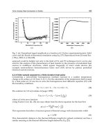
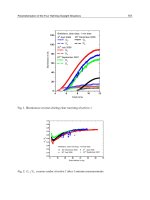
The results are summarized in Figure 13. It can be seen that, as expected, the Voc value
increases with the Δ(LUMO
A
– HOMO
D
). However, it can be seen also that two curve
families are clearly visible. One with small Voc values, which corresponds to cell
encapsulated without breaking the vacuum and another with higher Voc values, which
corresponds to cells encapsulated after 5 min of air exposure. The two curves are nearly
parallel, which demonstrates that the same phenomenon is at the origin of the Voc increase.
Since the only difference between these two families is the contact or not with room air, the
translation of the curve should be attributed to the presence of the thin natural Al
2
O
3
layer
at the electron acceptor/aluminium interface. This natural oxide does not depend on the
organic material but only on the alumium electrode air exposure, which is in good
agreement with the translation effect of the two curves. Such ultra thin Al
2
O
3
layer (1nm)
increases the shunt resistance value, which justifies the Voc value increase. Such effect of
aluminium oxidation on the open circuit voltage has already been proposed by Singh and
coll.[Singh et al., Appl. Phys. Lett., 2005; Singh et al., Sol. Energy Mater. Sol. Cells, 2006],
thanks to our in situ encapsulation process we have directly put this effect in evidence.
However, if the increase of the shunt resistance of the cells through insulating oxide
formation at the interface cathode/organic materiel, allows increasing the open circuit
Solar Energy
242
voltage and therefore the solar cells efficiency, the limit of the positive effect of such oxide
layer is rapidly achieved. Indeed, it is only efficient when electrons can tunnel through the
oxide layer. Beyond 2.5 nm, not only the shunt resistance increases but also the series
resistance and therefore the current and cell efficiency.
Moreover other limitation at the interface organic/cathode has been highlighted through the
experiments described below. It has been shown that one way for circumventing the
diffusion length limitation is to use cells with multiple interfaces. Peumans et al. [Peumans
et al., Appl. Phys. Lett., 2000] have shown that the introduction of a thin large band gap
organic material allows improving significantly the device performances. He called electron
blocking layer (EBL) this thin film, because its bandgap was substantially larger than those
of the organic donor and acceptor, which block excitons in the organic semiconducting layer
far from the cathode avoiding any quenching effect at the cathode/organic interface. Will
see more precisely the effect of this “EBL”, but first we will conclude on the effectiveness of
the very thin oxide layer between the cathode and the organic electron acceptor. In order to
discriminate between the effect of an EBL and an oxide layer deposited before the cathode
we have worked with ITO/CuPc/C
60
/Alq
3
/Al/P, Alq
3
being used as EBL layer. It is shown
in Table 1, that, as expected, the EBL improve significantly the cells performances, while the
encapsulation process does not modify the strongly the I-V characteristics.
Devices J
SC
(mA/cm
2
) Voc (V)
Rsh (Ω)
ITO/CuPc/C
60
/Al/PI 4.75 0.24 90
ITO/CuPc/C
60
/Al/PA 4.40 0.41 1650
ITO/CuPc/C
60
/Alq
3
/Al/PI 7.75 0.45 1800
ITO/CuPc/C
60
/Alq
3
/Al/PA 7.45 0.48 1850
Table 1. Jsc and Voc values of the different devices under AM1.5 conditions.
In fact, the Voc value in the presence of Alq
3
does not depend strongly on the encapsulation
process, while it does when simple CuPc/C
60
junction is used. This difference can be
explained by the variation of the value of the shunt resistance, Rsh. Without Alq
3
, a thin
Al
2
O
3
layer is necessary to improve Rsh and therefore Voc, with Alq
3
, Rsh is sufficient and
the alumina is not necessary to optimise the Voc value (Table 1).
Accordingly to the present discussion, the EBL is sufficient to confine the photogenerated
excitons to the domain near the interface where the dissociation takes place and prevents
parasitic exciton quenching at the photosensitive organic/electrode interface. Also it limits
the volume over which excitons may diffuse. For vapor deposited multilayer structures, a
significant increase in efficiency occurs upon the insertion of the exciton blocking interfacial
layer, interfacial layer, between the cathode and the electron acceptor film. Bathocuproine
(BCP) is often used as exciton blocking buffer layer [Peumans et al., Appl. Phys. Lett., 2000;
Huang et al., J.Appl. Phys., 2009]. However, with time, BCP tends to crystallize, which
induces some OSCs performance degradation [Song et al., Chem. Phys. Lett., 2005].
Consequently, either other more conductive [Refs] or more stable, e.g, aluminium tris(8-
hydroxyquinoline) (Alq
3
), materials have been tested as EBL [Song et al., Chem. Phys. Lett.,
2005; Hong, Huang and Zeng, Chem. Phys. Lett,., 2006; Bernède and al., Appl. Phys. Lett.,
2008]. Therefore, many organic materials with quite different HOMO and LUMO values can
be used as EBL. Indeed, it appears that EBL can also protect the electron accepting film from
atoms diffusion during deposition of the electrode. Also it is thick enough and sufficiently
Organic Solar Cells Performances Improvement Induced by Interface Buffer Layers
243
homogeneous to fill pinholes and others shorting effect which increases Rsh and therefore
Voc and the cell efficiency. Therefore the EBL protects the fragile organic films from damage
produced during electrode deposition onto the organic material. The large band gap of the
EBL, larger than that of the adjacent organic film, allows blocking the excitons in this film. If
the EBL blocks the excitons it should not block all charge carriers. Therefore the EBL should
be chosen so that it allows electrons collection at the cathode. However the offset energy of
the highest occupied molecular orbital (HOMO) of the electron donor (often the fullerene)
and the EBL (such as the bathocuproine) is large. Moreover, the optimum EBL thickness is
around 8 nm, which is too thick to allow high tunnelling current. So, even if the EBL is an
electron conducting material, the difference of the LUMO levels of C
60
and Alq
3
implies that
electrons must overcome a large energy barrier to reach the Al cathode in case of electron
transport via LUMO levels (Figure 14-1). More probably, the charge transport in the EBL is
due to damage induced during deposition of the cathode, which introduces conducting
levels below its LUMO (Figure 14-2) and explains the reason why the transport of electron is
not weakened. [Rand et al., Adv. Mater., 2005]. As a conclusion, the EBL, not only block the
excitons far from the cathode where they can be quenched, but also prevents damage of the
electron acceptor film during cathode deposition. It should be transparent to the solar
spectrum to act as a spacer between the photoactive region and the metallic cathode and it
must transport electrons to avoid high series resistance. The EBL is also important for
fabricating large-area devices with a low density of electrical shorts.
Fig. 14. Band schemes of organic films and cathode contact.
7. Anode/organic donor interface
Globally, the electrodes in contact with the organic materials have great importance in the
device behaviour. Of course, in optoelectronic devices it is necessary to allow the maximum
amount of photons of the solar spectrum to enter the active part of the device. Therefore it is
necessary that at least one of the electrodes should exhibit high transparency and should not
be reflecting. In classical configuration the transparent electrode, a transparent conductive
oxide thin film (TCO), is the anode. Typically, glass coated with the degenerate
semiconductor indium-tin oxide (ITO), is used as anode electrode. ITO, which commonly
serves as anode in organic optoelectronic devices, attracted considerable interest due to its
unique characteristics of high conductivity, good transparency in the visible domain and
easy patterning ability, moreover it is commercially available.
C
60
BCP Al
1
2
Solar Energy
244
A crucial point in organic devices is the interface between the inorganic electrodes and the
organic materials. The key parameter at the anode interface is the hole collection from the
organic semiconductor to the anode. A barrier for carrier transport is often present at the
interface. It is usually determined by the electrode/organic band offset, that is to say, in the
case of holes, the difference between the work function of the anode and the highest
occupied molecular orbital (HOMO) of the electron donor, even if, as discussed above, the
barrier height depends also of the presence, or not, of an interface dipole. About the
influence of the barrier height at the interface anode/organic donor Kang et al [Kang, Tan
and Silva, Organic Electronics, 2009] have shown a clear relation between the work function
of the anode and the devices performances. They show that the energy conversion efficiency
of the cells follows the variation of the value of the anode work function. The work function
was measured by Kelvin probe, the anode, ITO/PTFE (polytetrafluoroethylene), was treated
with different UV exposure time. The work function increases during the first five minutes
and then decreases, also the devices performances and mainly the short circuit current Jsc.
High Jsc in organic solar cells are mainly due to small barrier height between the anode and
the organic and subsequently improved carriers extraction process. Therefore, the influence
of the barrier height at the contact anode/electron donor being well established, it is
necessary to control the work function of the anode to achieve good band alignment and
ohmic contact. High work function anode is desirable to decrease the series resistance. High
and reproducible work functions are difficult to obtain for ITO [Bruner et al., J. Am. Chem.
Soc., 2002]. Many processes have been proposed to achieve this goal. First, as discussed in
paragraph 3, it should be underlined that ITO work function depends strongly of the thin
film history and it is quite difficult to predict. It has been shown that ITO surface chemistry
is difficult to control, because its surface is covered by hydrolysed oxides [Armstrong et al.,
Thin Solid Films, 2004), Donley et al., Langmuir (2002); Kim, Friend & Cacialli, J. Appl. Phys.,
1999]. In fact, he surface chemical functionality of ITO is not well understood [Katkova et al.,
Appl. Surf. Sciences, 2008]. Authors propose the presence of hydroxyl [Purvis et al., J. Am.
Chem. Soc,. (2000)] others not [Chaney & Pehrsson, Appl. Surf. Sci., 2003]. What is clear for all
experimenters in the field of organic optoelectronic devices is that cleanliness of the ITO
surface is critically important for efficient hole exchange at the organic material/ITO
interface. Devices performances, not only depend on the surface treatment but also on the
deposition batches [Berredjem et al., The European Physical Journal: Applied Physics, 2008].
Moreover, it is well known that crystals in polycrystalline ITO thin films have pyramidal
shape, which induces a significant surface roughness (some nm) of these films. This surface
roughness is often evocated as a source of leakage current and lifetime limitation in
optoelectronic devices. Also, ITO electrodes were reported to interact chemically, which
contributes to the degradation of optoelectronic devices performances [Kugleret al.,
Synthetic Metals, 1997)]. For instance, even in the absence of oxygen and moisture, oxidation
of organic material in contact with ITO has been reported [Scott et al., J. Appl. Phys.1997]. It
appears that ITO anode serves as source of oxygen. At least, it should be underlined that
ITO, is not ideal due to the scarcity of its main component: indium. Indeed, to day, ITO is
widely used as electrode in optoelectronic devices and demand for indium is expected to
outstrip supply these years, making devices based on ITO expensive. All that justifies, not
only the different works dedicated to ITO surface treatment itself, but also original works on
different TCOs and transparent anodes.
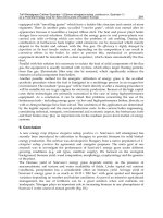
First of all different surface treatments of ITO have been probed. Hydrogen peroxide
treatment improves the devices performance through work function increase (4.7< Φ
M
< 4.8
Organic Solar Cells Performances Improvement Induced by Interface Buffer Layers
245
eV), however, even with similar Φ
M
, different turn-on voltage are measured. Obviously,
additional factors should be considered such as surface roughness performance [Kugleret
al., Synthetic Metals, 1997]. Different acidic solutions have been probed (HCl, H
3
PO
4
).
(a) (b)
Fig. 15. Surface structure of passivated ITO for acid (a) and base (b) treatment.
Treatments with phosphoric acid lead to an increase in work function of about 0.7 eV (4.5 to
5.2 eV) with good homogeneity [Johnev et al., Thin Solid Films, 2005)].
Such effect is induced by monolayer adsorption (Figure 15 a), which allows improving the
solar cells efficiency from 1.2 to 1.5 %.
However this efficiency remains smaller than that obtained with conducting polymer buffer
layer, which will be discussed below. When treated by a base a decrease of Φ
M
is obtained,
which means that Φ
M
can be shifted of 1 eV [Nüesch et al., Appl. Phys. Lett,. 74 1999].
Moreover, it is necessary to use an appropriate plasma treatment before chemical
adsorption. As a matter of fact, plasma treatments are often used to increase the ITO work
function. In the case of plasma treatment, after chemical pre-cleaning, the sample was
treated by RF plasma, usually the ambient gas is Ar or O
2
, with better results achieved with
O
2
. Not only the plasma treatment cleans the ITO surface, increases Φ
M
, but also smoothes
the film surface, whole things resulting in performance improvement of devices [Lu &
Yokoyama, Journ. Crys. Growth, 2004, Zhong & Jiang, Phys. Stat. Sol. (a), 2006]. Another well
known technique used to tune the ITO surface work function, is the deposition of self-
assembled monolayers (SAM) onto the ITO film surface. A SAM consists of a molecular
backbone terminated by an anchoring group and, at the other extremity, by an end group
that may induce a dipole, Δ
SAM
. Δ
SAM
is defined as positive if it up-shifts the vacuum level on
the organic/SAM side. Different organic material families can be used as SAM, tin
phenoxides [Bruner et al., J. Am. Chem. Soc., 2002], thiophene phosphonates , phosphonic
acids [Hansson et al., J. Am. Chem. Soc., 2005; Sharma et al., J. Appl. Phys., 2009], also
polymeric (LBL) assembly has been used for anode modification layer by layer [Kato, J. Am.
Chem. Soc., (2005].
If these chemical techniques allow tuning efficiently the work function of the ITO thin films,
physical techniques such as spin coating, vapor deposition can be used also with success.
The conducting polymer the most widely used to help the charge transporting at the
interface ITO/organic is the poly(ethylene dioxythiophene) doped with polystyrene sulfonic
acid (PEDOT:PSS) [Hoppe and Sariciftci, J. Mater. Res., 2004]. PEDOT:PSS is a p-type
semiconductor, a good hole transport material, it is soluble in water and easy to depose by
spin coating. Its work function is 5.2 eV.
Solar Energy
246
The initial solution of PEDOT-PSS is 3 wt. % in water. It is spun at 2000-5000 rpm to form a
50-100 nm thick layer. After deposition, to prevent the presence of water in the device,
PEDOT:PSS coated ITO is annealed for half to an hour at 100-150°C. Then the different
organic constituents and the cathode of the optoelectronic device are deposited. The
PEDOT:PSS buffer layer allows the device performance to be significantly improved, OLEDs
and solar cells. It is admitted that the high value of its work function allows a good band
alignment with the HOMO of the electron donor, which decreases the barrier height at the
interface and therefore assures a better hole collection from the polymer into the ITO
electrode. Also it is supposed that the PEDOT:PSS spin coated onto the ITO surface
smoothes its surface and, therefore, any possible short circuiting due to the spiky roughness
of the ITO surface is prevented. It improves the contact between the polymer and the ITO. It
is admitted that this buffer layer enhances adhesion to the organic layer. Also it prevents
direct contact between the oxygen of the ITO and the organic material.
However, PEDOT:PSS is problematic since its poor conductivity is a major limiting factor
for device performance and it degrades under UV illumination [Chang & Chen, Appl. Phys.
Lett,. 2007; Kang et al., J. Phys. D: Appl. Phys., 2008]. Even after baking, due to its hygroscopic
nature some amount of water always appears in PEDOT:PSS, which introduces water into
the active layer, it is also slightly acidic
[Van de Lagemaat et al., Appl. Phys. Lett., 2006,
Johnev et al., Thin Solid Films, 2005]. Moreover, not only the depositing process from
aqueous solution introduces impurities but the reproducibility is in need of improvement
[Johnev et al., Thin Solid Films, 2005].
Therefore, other solutions have been proposed, each one based on original buffer layers
such as metal or oxides. Some attempts using thin metal buffer layers have been done
during the last years, however the results were quite disappointing, the metal thin film used
being thick of some nanometers, the transmission of the visible light decreases significantly
(Figure 16) and also the devices efficiency [Yoo et al., Synthetic Metals, 2005].
400 600 800 1000 1200 1400 1600 1800 2000
20
40
60
80
100
T (%)
λ (nm)
ITO
ITO/Au 0,5 nm
ITO/Au 1,0 nm
ITO/Au 1,5 nm
Fig. 16. Variation of the transmittance of ITO/Au structures with the Au thickness (0 to 1.5
nm).
Organic Solar Cells Performances Improvement Induced by Interface Buffer Layers
247
We have shown that this difficulty could be overcome by using an ultra thin (0.5 nm) gold
film. The introduction of this ultra-thin metal layer at the interface anode/electron donor
allows improving significantly the energy conversion efficiency of the organic solar cells
[Bernède et al., Appl. Phys. Lett., 2008; Bernède et al., Sol. Energy Mater. Sol. Cells, 2008].
Fig. 17. Schematic structure of the fabricated solar cells with the ultra-thin gold layer onto
the TCO.
The efficiency improvement is even more remarkable as regards to TCO initial quality. The
effect of this ultra-thin metal buffer layer has been probed on multi-heterojunction organic
solar cells (Figure 17) and we present, with more details, this example of efficient buffer
layer at the interface anode/electron donor. The electron donor used was copper
phthalocyanine (CuPc) (some attempts have been done using pentacene and similar
behaviour has been obtained), the electron acceptor was fullerene (C
60
) and the electron
blocking layer was the tris(8-hydroxyquinoline) (Alq
3
) [Kim et al., Sciences, 2007, Berredjem
et al., Eur. Phys. Journ.: App. Phys. 2007]. CuPc, C
60
and Alq
3
have been deposited in a
vacuum of 10
-4
Pa. The thin film deposition rate and thickness were estimated in situ with a
quartz monitor. The deposition rate and final thickness were 0.05 nm/s and 35 nm in the
case of CuPc, 0.05 nm/s and.40 nm in the case of C
60
and 0.1 and 9 nm for Alq
3
. These
thicknesses have been chosen after optimisation.
After organic thin film deposition, the aluminium upper electrodes were thermally
evaporated, without breaking the vacuum, through a mask with 2 mm x 8 mm active area.
This Al film behaves as the cathode, while the ITO is the anode. Some ITO anodes have been
covered with an ultra thin metal film deposited by vacuum evaporation, the metal being Au,
Cu, Ni. The thickness of these ultra thin metal films, M, has been varied from 0.3 to 1.2 nm.
Finally, the structures used were: glass/ITO(100nm)/M (0≤x≤1.2
nm)/CuPc(35nm)/C
60
(40nm)/Alq
3
(9 nm)/Al(120nm). It can be seen in figure 18 and table 2
that the presence of the ultra-thin gold layer improves significantly the solar cells
performances. When different batches of ITO were used, without Au buffer layer, the solar
cells performance vary strongly, while they were of the same order of magnitude when an
ultra-thin gold layer was deposited onto ITO (Table 2).
Similar results have been obtained when AZO and FTO are used. The performances of
organic solar cells using this ultra thin metal layer, are nearly similar, whatever the TCO
used [Bernède et al., Appl. Phys. Lett., 2008, Bernède et al., Sol. Energy Mater. Sol. Cells, 2008].
This suggests that indium free organic devices with high-efficiency can be achieved, which
can contribute to the sustainable development.
Solar Energy
248
Batch Anode Jsc (mA/cm
2
) Vco (V) FF η %
ITO 7.31 0.45 0.44 1.45
a
ITO/Au (0.5nm) 8.09 0.49 0.56 2.25
ITO 6.80 0.40 0.25 0.67
b
ITO/Au (0.5nm) 8.34 0.45 0.50 1.86
Table 2. Photovoltaic performance data of devices achieved with batches a and b of ITO,
under AM1.5 conditions.
0,0 0,2 0,4 0,6
-10
0
10
J (mA/cm
2
)
V (V)
b-ITO in the dark
b-ITO under ligth
b-ITO/Au in the dark
b-ITO/Au under ligth
ITO/Au
ITO
Kink effect
Fig. 18. Typical J-V characteristics of solar cells, with an anode of ITO (batch b) covered (▼)
or not (●) with 0.5 nm of Au, in the dark (open symbol) and under illumination of AM1.5
solar simulation (100 mW/cm
2
) (full symbol).
As said above, others metal such as Cu, Ni, Ag, Pt have been probed, however, up to now,
the best results have been obtained with a gold ultra thin film. It should be noted that,
roughly, the organic solar cells performance increases with the metal work function, which
means that, Ag which have the smallest Φ
M
gives the worst performances.
In order to understand the ultra-thin gold layer effect, TCO covered with such gold layers
have been characterized by scanning electron microscopy (SEM), atomic force microscope
(AFP), X-ray photo-electron spectroscopy, optical transmission measurement (Figures 16, 19).
It is shown that the ultra-thin film is discontinuous, while the roughness of the TCO/Au
electrode is not different from that of bare TCO (0.8 nm). However it can be seen through the
XPS study that the CuPc has grown more homogeneously when deposited onto gold covered
TCO. Moreover as shown in Figure 18 the shape of the J-V characteristic depends on the anode
configuration, in the case of bare TCO a “kink” effect is clearly visible, while classical diode
characteristics are obtained when the TCO is covered by the ultra-thin gold layer.
In order to discuss the effect of the ultra thin gold film on solar cells performances, we recall
shortly supposed beneficial effect of the classical buffer layer, the PEDOT:PSS.
As said above, up to now, the most common buffer layer inserted at this interface is the
PEDOT:PSS, its contribution to the improvement of solar cells performance has been
attributed to:
Organic Solar Cells Performances Improvement Induced by Interface Buffer Layers
249
a-ITO (rms = 0.80 nm)
b-ITO/Au (rms = 0.75 nm)
Fig. 19. AFM images of Au (0.5 nm) covered ITO (a) and bare ITO (b).
• the smoothing effect of the quite rough TCO surface, therefore, any possible short
circuiting due to the spiky roughness of the TCO surface is prevented.
•
the physical separation, which avoids direct contact between the oxygen of the TCO
and the organic material.
•
its work function (φ
M(PEDOT: PSS)
= 5.1 eV), which allows to decrease the barrier height at
the interface, since the work function of the TCO is smaller (4.5-4.7 eV for ITO), while
the HOMO of CuPc is 5.2 eV.
•
the improvement of the contact between the polymer and the TCO. It is admitted that
this buffer layer enhances adhesion to the organic layer.
It can be seen immediately that the two first contributions can be excluded when an ultra-
thin gold film is substituted by PEDOT:PSS, since the roughness of the modified anode is
similar to that of the initial TCO and the gold film is discontinuous. The two last
contributions seem more probable. The work function of gold is 5.1 eV and therefore the
ultra-thin gold layer can improve the matching between the work function of the anode and
the highest occupied molecular orbital (HOMO) of the organic electron donor (Figure 5a, b,
c). Such contribution will be discussed more carefully below. The fourth contribution is in
good agreement with the XPS study, which shows that the CuPc films are more
homogeneous when deposited onto gold modified TCO.
Therefore from the examples presented above it can be concluded that the two main
contributions to the interface improvement by inserting an ultra-thin metal buffer layer
between the TCO anode and the CuPc are a better matching of the band structure (Figure
20) and a higher homogeneity of the organic film.
The equivalent circuit model (figure 5 a) could be helpful in understanding of organic solar
cells by providing a quantitative estimation for losses in the cells. As said above, the
equivalent circuit commonly used to interpret the I-V characteristics of real solar cells
consists of a photogenerator connected in parallel with a diode and a shunt resistance, and a
series resistance. For such solar cells the mathematical description of this circuit is given by
the equation (1).
Solar Energy
250
(a) (b)
Fig. 20. Contact anode (ITO)/ electron donor (CuPc)
a-without buffer layer; b-with a gold buffer layer.
0,00,10,20,30,40,50,60,70,8
-2,0x10
-3
0,0
2,0x10
-3
4,0x10
-3
6,0x10
-3
8,0x10
-3
1,0x10
-2
I (A)
V (V)
ITO/Au anode
Theorical
Experimental
a
0,0 0,2 0,4 0,6 0,8
-1,5x10
-3
-1,0x10
-3
-5,0x10
-4
0,0
5,0x10
-4
1,0x10
-3
I (A)
V (V)
ITO anode
Theorical
Experimental
b
Fig. 21. I-V characteristics under AM1.5 illumination of a solar cell using a ITO/Au anode
(a) and a ITO anode (b), (●) experimental and (■) theoretical curves.
Organic Solar Cells Performances Improvement Induced by Interface Buffer Layers
251
In a recent contribution [Kouskoussa et al., Phys. Stat. Sol. (a), 2009], we have shown that the
Lambert W-function method can be used to determinate Rs, the series resistance, Rsh the
shunt resistance, n the ideality factor of the diode and Iph the photo-generated current.
The problem to be solved is the evaluation of a set of five parameters Rs, Rsh, n, Iph and Is
in order to fit a given experimental I-Vcharacteristics using a simple diode circuit.
A good agreement between the experimental and theoretical fitted curves is achieved with
ITO/Au anode (Figure 21 a), while it is not in the case of bare ITO anode.
As said above no agreement could be achieved in the case of a bare ITO or Ag covered
anode, whatever the series and shunt resistance proposed. Such impossibility shows that the
simple equivalent scheme used in this theoretical study cannot explain the experimental
results obtained with a bare ITO anode.
In the case of bare and Ag covered ITO anode, it is necessary to assume the presence of a
back-contact barrier at the ITO/CuPc interface (figure 5 b), to achieve a good fit between
experimental and theoretical results. Assuming a thermoionic current at this interface, the
hole current is:
I
b
= - I
b0
(exp(-qV
b
/kT)-1) (10)
With: - I
b0
saturation current,
- V
b
voltage across the back contact,
- k Boltzmann constant,
- T temperature.
Therefore the current-limiting effect, “rollover”, is due to the back-contact barrier height. It
occurs because the total current saturate at a value J
b0
[Demtsu and Sites, Thin Solid Films,
2006]. The value of J
b0
is the current value where the J-V curve starts to show rollover.
Demtsu and Sites have treated the main junction and the back-contact junction (Figure 6 b)
as independent circuit element. Here, when a forward bias V is applied to the circuit, the
voltage is divided between V
m
across the main CuPc/C
60
junction, V
b
across the back-
junction TCO/CuPc and IRs across the series resistance:
V = V
m
+ V
b
+ IRs.
Under illumination the current across the main junction is:
I
m
= I
m0
(exp(qV
m
/nkT)-1) – Iph + Vm/Rsh (11)
And through the back contact it is:
I
b
= - I
b0
(exp(-qV
b
/kT)-1) + Vb/ R
b
sh
(12)
Equating equations (10) and (11):
I
m0
(exp(qV
m
/nkT)-1) – Iph + Vm/Rsh + I
b0
(exp(-qV
b
/kT)-1) - Vb/ R
b
sh
= 0 (13).
The parameters Rs and I
m0
, n, Rsh of the main diode are calculated in the region far from the
saturation current Ib. As said above, I
b0
is the current value where the J-V curve starts to
show rollover. Then equation (13) can be solved.
A good agreement can be achieved between experimental and theoretical curves, (Figure 21
b), which validates the hypothesis of the presence of a rectifying effect at the ITO/CuPc
contact.
Solar Energy
252
The parameters extracted are reported in Table 3. It should be noted that when ITO is
covered with Ag, two diodes are necessary to obtain a good fit between the experimental
and theoretical curves. Since the work function of Ag is only 4.3 eV, this result is in good
agreement with the present discussion. One can see in Table 3 that, when the two diodes
model is used, the estimated Rs values are of the same order of magnitude as those of
ITO/Au anode. Therefore the introduction of a back junction diode is a good interpretation
of the interface ITO/CuPc. It justifies the small fill factor and short circuit current values
when bare ITO is used as anode in the heterojunction solar cells. The Voc value can be
improved thought an increase of the shunt resistance value. It can be seen in Table 3 that the
shunt resistance value of the cells with a ITO/Au anode is significantly higher.
Anode Main junction CuPc/C
60
Back-contact junction
n Rsh Rs I
mo
(A) R
b
sh
(Ω)) I
bo
(A)
ITO 2.55 330 20 2 10
-6
15000 2.58 10
-6
ITO/Ag 2.6 400 40 1 10
-6
13200 2.24 10
-6
ITO/Au 1.5 6900 25 2.23 10
-9
- -
Table 3. Parameters calculated using a main diode and (or not) a back contact diode.
Table 3 shows that the ideality factor, n, decreases, while Rsh increases, when the ITO anode
is covered by an ultra-thin Au layer, which corresponds to a significant improvement of cell
performance. When Ag is used the improvement is not significant. The increase of Rsh can
be related to the growth of pinhole free organic films when deposited onto Au coated TCO
[Kim et al., Sol. Energy Mater. Sol. Cells, 2009].
When thicker metal films are introduced at the anode/organic interface, surface plasmon
effect has been proposed as alternative approach toward enhanced light absorption without
the need for thick films. [Chen, et al., Appl. Phys. Lett., 2009]. A surface plasmon is an
optically generated wave, which propagates along a metal/dielectric interface. In tuning the
light excitation, a resonance can occur when the frequency of the incident photon equals the
collective oscillation frequency of conduction electrons of metallic particles. These properties
can be used in the photovoltaic domain in order to improve the light absorption. Theoretical
calculations have been performed to determine optimal plasmonic materials to optimise
light absorption [Duche, et al. Sol. Energy Mater. Sol. Cells, 2009]. Enhanced absorbance up to
50% has been experimentally obtained in a 50 nm thick blend film including silver
nanospheres with a diameter of 40 nm. Devices based on BHJ structures using ITO anode
covered with Ag nanodots permits 20% improvement of the efficiency [Kim et al., Appl. Phys.
Lett., 2008]. The plasmon resonance wavelength depends on the metal nanodots properties, it
can be tuned by annealing the silver film or using other metal [Morfa,. Appl. Phys. Lett., 2008].
Even if the efficiency of the surface plasmon effect in the field of solar cells is always under
discussion, it is often proposed to improve the light absorption.
After metals, different oxides (MoO
3
, WO
3
, ZnO) have been probed as buffer layer at the
TCO anode /CuPc interface.
In the case of OLEDs [Im et al., Thin Solid Film, 2007; Hsu & Wu, Appl. Phys. Lett., 2004; Shi,
Ma, and Peng, Eur. Phys. J. Appl. Phys., 2007; Qiu et al., J. Appl. Phys., 2003;
Matsushima et al., Appl. Phys. Lett., 2007; Jiang et al., J. Phys. D: Appl. Phys., 2007; You et al., J.
Appl. Phys., 2007] and organic thin film transistors [Chu et al., Appl. Phys. Lett., 2005;
Park, Noh and Lee, Appl. Phys. Lett., 2006], different attempts have been done, with some
success, using different oxide thin films as buffer layer between the TCO and the organic
Organic Solar Cells Performances Improvement Induced by Interface Buffer Layers
253
material. Also some attempts have been probed in the case of organic solar cells [Yoo et al.,
Synthetic Metals, 2005; Chan et al., J. Appl. Phys., 2006]. The use of such buffer layer is based
on the idea that the potential barrier at the ITO/organic donor interface can be reduced by
elevation of ITO surface work function, giving high hole transport at this interface. In order
to check this hypothesis, using the same multiheterojunctions as above, we have probed
different buffer layers at the ITO/CuPc interface. The buffer layers used were MoO
3
, WO
3
and ZnO. The resulting different I-V characteristics are compared to those of a reference cell
built on untreated anode. The different energy band diagrams are proposed and discussed.
Finally, we demonstrate that the reduction process of the barrier at the ITO/organic donor
interface depends on the type of material: oxide or metal.
During this study, the majority of the ITO anodes have been covered with an oxide buffer
layer. These thin buffer layers were deposited by vacuum evaporation. The MoO
3
oxide thin
films were thermally evaporated onto the ITO coated glass. The thickness of these ultra thin
oxide films ranged between 1 and 7.
Finally, the structures used were:
glass/ITO(100nm)/bufferlayer/CuPc(40nm)/C
60
(40nm)/Alq
3
(9nm)/Al(120nm)/P
Se
.
The optimum efficiencies were achieved for thickness of around 3.5 ± 1 nm, that means that,
as in the case of gold, the oxide film does not completely cover the anode surface since it has
been shown that 5 nm are necessary to obtain continuous thin MoO
3
film, using thermal
evaporation [Song et al., Chem. Phys. Lett.,2005]. For thicker oxide films, if the fill factor (FF)
stays far higher than the value obtained with bare ITO, the short circuit current (Jsc) is
slightly smaller and it progressively decreases as the oxide thickness increases. With thinner
oxide films the inflection point, in the J-V characteristics, typical of the bare ITO anode
(Figure 22), is still slightly present.
-0,2 0,0 0,2 0,4 0,6
-5,0
-2,5
0,0
2,5
5,0
J (mA/cm
2
)
V (V)
ITO
ITO
ITO/MoO
3
(6 nm)
ITO/MoO
3
(6 nm)
ITO/MoO
3
(3 nm)
ITO/MoO
3
(3 nm)
Anode:
Under AM 1.5
In the dark
Fig. 22. Typical J-V characteristics of Anode/CuPc/C
60
/Alq
3
/Al structure, with Anode =
ITO (●), ITO/MoO
3
(6 nm) (■) and ITO/MoO
3
(3 nm) (▲), in the dark (full symbol) and
under illumination of AM1.5 solar simulation (100 mW/cm
2
) (open symbol).
Solar Energy
254
It should be highlighted that the main improvement induced by the oxide is related to the
fill factor (Table 4). Here also the improvement induced by the oxide does not depend on the
TCO used, since the best result achieved by the cells deposited during the run corresponds
to FTO. Here also the presence, or not, of the kink effect testifies of the efficiency of oxide.
A similar approach to the one used in the case of gold buffer layer can be used in the case of
oxide buffer layer. Often the positive effect on the properties of the organic optoelectronic
devices of the anode buffer layer is mainly attributed to the reduction of the barrier energy
between the ITO, which is usually the anode, and the organic layer (electron donor for solar
cells, hole transporting layer for OLEDs ).
Anode ITO ITO/MoO
3
(6 nm) ITO/MoO
3
(3 nm)
Jsc (mA/cm
2
) 4.69 3.90 5.05
Voc (V) 0.41 0.46 0.45
η (%) 0.73 0.97 1.13
FF (%) 38 54 49.7
Table 4. Photovoltaic performance data under AM1.5 conditions of devices using ITO,
ITO/MoO
3
(3 nm) and ITO/MoO
3
(6 nm) anodes.
Fig. 23. Band scheme before contact
If the buffer layer material exhibits a high work function value (Figure 23), i.e., a work
function in good agreement with the HOMO of the organic layer, it is often suggested that
there is a simple alignment of the energetic levels of the anode and the organic material,
without any discussion of the electrical properties of the buffer layer. However the electrical
behavior of conductive, semi conducting and insulating materials is very different and
therefore the nature of their interfaces will depend on the their properties.
HOMO
(5.2 eV)
Φ
S
LUMO
(3.5 eV)
Φ
ITO
4.5 eV
ITO Au MoO
3
CuPc
5.1 eV
Φ
Au
5.4 eV
V
Β
Mo
Organic Solar Cells Performances Improvement Induced by Interface Buffer Layers
255
If we introduce an insulating film, (I), between the metal, (M) (or degenerated
semiconductor), and the semiconductor, (S), the contact behaves like a MIS structure. This
means that there is not band alignment between the TCO, the insulating layer and the
organic semiconductor but, qualitatively, the band diagram of Figure 24. This results from
the fact that the Fermi level must be constant throughout the metal/insulating layer/semi-
conductor and therefore [Demtsu et Sites, Thin Solid Films, 2006]:
Φ
b°
=Φ
b
+ Δ (15)
The distribution between Φ
b
and Δ depends on the insulating properties of the oxide and the
semiconductor properties. The space charge, which forms in the depletion layer of the
semiconductor, can be expressed as an equivalent surface state density Qsc. In the ideal
case, that is to say in the absence of any space charge effect in the interfacial insulating layer,
an exactly equal and opposite charge Qm develops on the metal surface. In this case of an
ideal insulating layer the potential Δ across the interfacial layer can be obtained, following
the application of Gauss law to the surface charge on the metal and semiconductor:
Δ = δ(Qm/ε
i
) (16)
ε
i
being the dielectric constant of the insulating layer and δ its thickness [Sze, Physics of
Semiconductor Devices, John Wiley Editor, 1981]. Therefore, even if there is not a simple
alignment of the work function of the insulating film with those of the conductive anode
and of the semiconductor, the presence of this layer can significantly modifies the barrier
value at the interface through the potential Δ [Park, Noh and Lee, Appl. Phys. Lett, 2006]. As
a summary, in the case of the present work, since we have (Figure 23): Φ
ITO
= 4.5 eV, Φ
Au
=
5.1 eV, HOMO
CuPc
= 5.2 eV, VB
MoO3
= 5.4 eV.
-
the ITO/CuPc contact induces a pseudo Schottky contact, V
bi
= φ
M
- φ
S
between 0.5 and
0.7 eV, CuPc being an electron donor (p-type semiconductor), φ
S
is slightly smaller than
HOMO
CuPc
(Figure 20 a), while the Au/CuPc, and therefore ITO/Au/CuPc, contacts
induce a nearly ohmic contact (Figure 20 b).
-
the ITO/MoO
3
/CuPc behaves like a MIS structure, that is to say the insulating layer
induces a decrease of the barrier height with Φ
b
= Φ
b°
- Δ [ Cowley and Sze, J. Appl.
Phys., 1965]. As discussed above the efficiency of the insulating layer in the band
alignment depends on the insulating properties and the thickness of the MoO
3
layer
(Figure 24).
We have now all the keys necessary to explain the behaviour of the different cells studied in
the present work. It is well known that a barrier is present at the interface ITO/organic
material (electron donor in the case of solar cells and hole transporting layer in the case of
OLEDs). The introduction of an interfacial layer between the ITO and the organic material
allows to decrease the barrier height at the interface, which facilitate the hole collection
(solar cells) or hole injection (OLEDs). It is clear from the discussion above that an oxide or a
metal with sufficiently high work function value should be used.
MoO
3
has already been used to increase the hole injection in OLEDs [Matsushima et al.,
Appl. Phys. Lett., 2007; Jiang et al., J. Phys. D: Appl. Phys., 2007]. The decrease in the barrier
height, allowed by the introduction of a MoO
3
layer, increases with its thickness (equation
16). However, as shown by the experimental study, there is an optimum thickness value.
Solar Energy
256
When the film is too thin (≤ 1.5 nm) the Δ value is small and moreover the covering
efficiency of the ITO by the MoO
3
is not complete. For MoO
3
layers thicker than 6 nm, the
short circuit current significantly decreases (Figure 22).
In Figure 24 it is supposed that the carriers cross the insulating layer by tunnel effect. The
interfacial buffer layer is assumed to be a few angstroms thick and transparent to carriers
whose energy is greater than the potential barrier of the semiconductor. However, when the
thickness of the insulating layer increases, the probability of tunnel effect decreases. It is
admitted that up to 3 nm the efficiency of the tunnel effect is maximum, while it decreases
progressively for thicker films.
We have shown that the optimum MoO
3
thickness is around 3.5± 1 nm, which means that
the insulating layer is efficient even for thickness higher than the theoretical optimum value.
However evaporated molybdenum oxide films are strongly oxygen deficient and Rozzi et al
have shown, in a theoretical study, that, when some oxygen is removed from the MoO
3
crystal, some Mo4d antibonding orbitals located in the gap are filled up [Rozzi et al., Phys.
Rev., 2003]. Therefore holes can cross the insulating film by multiple tunnelling steps [A.G.
Milnes, D.L. Feucht, ”Heterojunctions and metal semi-conductor junctions.”, Academic
Press Editor, 1972.] effect through these gap states introduced by the oxygen vacancies. As a
result, the probability of tunnelling though the barrier increases. Finally the optimum MoO
3
thin film thickness, 3.5± 1 nm, corresponds to a compromise between an optimum ITO
coverage and a sufficient transparency to charge carriers.
Fig. 24. Band scheme after contact: Hole transfer from the organic electron donor to the
anode for different anode configurations after contact.
8. Example of the effect of an organic buffer layer used in different
configurations
Factors which limit organic solar cells performance include limited spectral sensitivity,
carriers separation at the interface acceptor/donor, low carrier mobility, energy step at the
organic material/electrode. In devices based on ED/EA heterojunction, the theoretically
obtainable open circuit potential (Voc) is given by the difference between the highest
occupied molecular orbital of the electron donor (HOMO
D
) and the lowest unoccupied
molecular orbital of the electron acceptor (LUMO
A
): Δ (HOMO
D
-LUMO
A
)
[Zimmermann et al., Thin Solid Films 2005]. The introduction, at the electron donor /electron
acceptor interface, of an ultra-thin organic layer could allows controlling the Voc value by
modifying this difference as shown by Kinoshita and col. [Kinoshita et al., Appl. Phys. Lett.,
2007]. They use with success this multicharge separation interface concept to increase the
Voc value. They introduce an ultra-thin CuPc layer, which is usually used as electron donor,
at the pentacene/fullerene interface. CuPc has also been proved to be an efficient buffer
TCO MoO
3
CuPc
Δ
Organic Solar Cells Performances Improvement Induced by Interface Buffer Layers
257
layer [Hong, Huang, and Zeng, Chem. Phys. Lett., 2006]. In order to improve carrier mobility,
structural templating of CuPc has been obtained using an ultra-thin 3,4,9,10-
perylenetetracarboxyl dianhydride interlayer [Sullivan, Jones and Ferguson, Appl. Phys.
Lett., 2007]. In the present example, similar experiments have been done with a perylene
derivative:N,N’–diheptyl-3,4,9,10-perylenebiscarboximide (PTCDI-C7).
8.1 Synthesis of the N,N’–diheptyl-3,4,9,10-perylenebiscarboximide (PTCDI-C7)
PTCDI-C7 (Figure 25) was synthesized by condensation of PTCDA with heptylamine
[Demmig and Langhals, Chem. Ber., 1988]. This compound is sufficiently soluble in
chloroform to allow a chromatographic method for purification. Yield: 85 %. The elemental
microanalyses results are in good agreement with the expected ones (weight %: C = 77.76; H
= 6.74; N = 5.11).
N
N
O
O
O
O
C
7
H
15
C
7
H
15
Fig. 25. PTCDI-C7 molecule.
8.2 Organic solar cells realisation
In the present series of experiments, the TCO electrode was a layer of indium tin oxide (ITO)
on glass substrate. CuPc, PTCDI-C7, C
60
and Alq
3
have been deposited in a vacuum of 10
-4
Pa. The thin film deposition rate and thickness were estimated in situ with a quartz monitor.
The deposition rate and final thickness were 0.05 nm/s, 35 nm for CuPc, 0.05 nm/s and 40
nm in the case of PTCDI-C7 and or C
60
and 0.05 nm/s and 8 nm for Alq
3
. The thicknesses
have been chosen after optimisation.
We have shown earlier that the presence of an ultra-thin metallic film at the TCO/organic
material interface allows improving significantly the power conversion efficiency of organic
solar cells [Bernède et al., Appl. Phys. Lett., 2008]. So, a very thin Au film (0.5 nm) has been
introduced at the interface ITO/CuPc in the most cases. The thickness of the organic films
has been checked with a scanning electron microscope (SEM). After organic thin film
deposition, aluminium upper electrodes were thermally evaporated (150 nm thick), without
breaking the vacuum, through a mask with 1.5 mm x 6 mm active area.
8.3 Experimental tests and discussion of the effect of PTCDI-C7 buffer layers
As justified above, PTCDI-C7 has been probed as a buffer layer at the CuPc/C
60
and
anode/electron donor interfaces. Following the multicharge separation interfaces concept,