Radio Frequency Identification Fundamentals and Applications, Design Methods and Solutions Part 2 ppt
Bạn đang xem bản rút gọn của tài liệu. Xem và tải ngay bản đầy đủ của tài liệu tại đây (1.36 MB, 25 trang )
Design Considerations for the Digital Core of a C1G2 RFID Tag
17
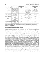
Fig. 2. Architecture of the low power C1G2 digital core.
Working state
STRTP STDBY RX CNTRL TX
PM
ON ON ON ON ON
Symbol detector
OFF ON ON OFF OFF
Command decoder
OFF OFF ON OFF OFF
Control
ON OFF OFF ON OFF
Memory access
ON OFF ON ON ON
VEEPROM
ON OFF OFF ON OFF
TX
OFF OFF OFF OFF ON
Table 1. Working states of the digital core.
transmission. In this state only the symbol detector is active. When the beginning of a new
message from the reader is detected, the command decoder is activated and the working
state turns to RX. After receiving the whole message, the working state changes to CTRL,
deactivating the command decoder and the symbol detector, and activating the control and
the register bank. Finally, in the TX state the response is sent to the reader and the working
state returns to STDBY.
Reading from the EEPROM is one of the most power hungry operations that the tag
performs. In the design presented in this chapter, the EEPROM is read when a lot of energy
is arriving to the tag. Then, the read data is stored in VEEPROM, which is less power
hungry. This way, if data from the EEPROM is needed when less energy is available, they
can be read from VEEPROM instead of from EEPROM. The introduction of this module
allows reshaping the power distribution so that the power peaks caused by the accesses to
EEPROM can be moved to less critical time intervals. In exchange, the tag spends more time
initializing, as it must copy the data from the EEPROM to the VEEPROM.
Radio Frequency Identification Fundamentals and Applications, Design Methods and Solutions
18
3. Analysis of the clock signal requirements
As the power consumption of the digital core grows with the clock frequency, the selection
of a minimum clock frequency will maximize the communication range. In the following, a
detailed study of the clock signal constraints for C1G2 communication is presented. This
study shows that the minimum required clock frequency depends on the characteristics of
of the clock signal and the implementation of the transmitter.
The section is organized as follows. First, a model for the clock signal used by the digital
core is defined. Then, the operation of the digital core is analyzed together with the
specification of the standard. From this analysis, equations that constrain the clock signal
parameters are obtained. These equations are computed numerically to find the regions in
the clock signal parameter space where the C1G2 standard specifications are satisfied. These
results facilitate the definition of the requirements for the generator of the clock signal used
in the digital core.
3.1 Clock model
Ideally, the clock signal can be considered as a square wave of period T. The frequency,
f=1/T, is assumed to be constant and invariable in time. Nevertheless, actual clock sources
do not generate perfect clock signals. For instance, if we measure the average clock period
over two time intervals in different days or ambient conditions, the results may be different.
Moreover, the duration of the clock periods within the same time interval suffers small
variations from one cycle to another. For our analysis, we will model the clock signal using
two parameters:
Average period, T
a
: it is the mean value of the period of the clock signal during a whole
inventory round.
Random jitter, ξ
i
: it is a random variable that represents the normalized deviation of the
clock edges from the edges of the average period.
Thus, the duration of the ith clock period T
i
is given by T
i
=T
a
+ξ
i
. If the maximum random
jitter of the clock signal is annotated as ξ
max
, then for all i, T
i
∈ [T
a
·(1-ξ
max
), T
a
·(1+ξ
max
)]
3.2 Forward link
In the forward link of C1G2 (EPC Global, 2005), a reader communicates with one or more
tags by modulating a Radio Frequency (RF) carrier using Amplitude-Shift Keying (ASK)
modulation with Pulse Interval Encoding (PIE). The reader transmits symbols of duration
T
S
=T
H
+T
L
. In each symbol, the signal has maximum amplitude during T
H
seconds and
minimum amplitude during T
L
seconds. T
L
=PW for both a data-0 and a data-1. As shown in
Fig. 3, in order to transmit a data-0, T
H
is set so that T
S
=Tari. In order to transmit a data-1, T
H
is set so that 1.5·Tari ≤T
S
≤2·Tari.
Fig. 3. PIE codification, from (EPC Global, 2005).
Design Considerations for the Digital Core of a C1G2 RFID Tag
19
The forward data rate is set in the preamble of every command sent by the reader to the tag
by means of symbol RTcal, as shown in Fig. 4. The duration of this symbol RTcal is equal to
the duration of a data-0 plus the duration of a data-1. A tag shall measure the length of RTcal
and compute pivot=RTcal/2. The tag shall interpret subsequent reader symbols shorter than
pivot as data-0s, and subsequent reader symbols longer than pivot as data-1s.
Fig. 4. Forward link calibration in the preamble, from (EPC Global, 2005).
3.2.1 Symbol detection
The front-end of the tag is assumed to have a one bit Analog to Digital Converter (ADC) to
convert the envelope of the RF signal to a digital signal. The input to the digital core is
assumed to have a high value during T
H
and a low value during T
L
. The digital core samples
the input signal and identifies the incoming symbols by measuring the distance between
modulated pulses. It is assumed that one sample is taken every clock cycle.
Given a generic symbol S, its duration will be annotated as t
S
. The number of samples
obtained when sampling S, n
S
, will be in the range defined by equation (4).
max max
(1 ) (1 )
SS
S
aa
tt
n
TT
ξξ
⎢
⎥⎡ ⎤
≤≤
⎢
⎥⎢ ⎥
⋅+ ⋅−
⎣
⎦⎢ ⎥
, (4)
where
⎣⋅⎦ and ⎡⋅⎤ are the floor and the ceil functions respectively.
3.2.2 Forward link constraints
For proper operation, the digital core shall be able to detect when its input signal is in the
high and in the low states. The duration in the low state, PW, is the shortest one. Therefore,
the first constraint is that n
PW
≥1. From (4), the first constraint is obtained:
max
1
(1 )
a
PW
T
ξ
⎢⎥
≥
⎢⎥
⋅+
⎣⎦
. (5)
The second constraint comes from the fact that in order to detect the data-0 symbol properly,
the number of samples obtained from a data-0 symbol has to be lower or equal to
n
pivot
: n
data-0
≤n
pivot
, where n
pivot
=⎣n
RTcal
/2⎦. Using (4) to obtain the maximum number of
samples for n
data-0
and the minimum number of samples for n
RTcal
, we have,
max max
1
(1 ) 2 (1 )
aa
Tari RTcal
TT
ξξ
⎢
⎥
⎡
⎤⎢ ⎥
≤
⎢
⎥
⎢
⎥⎢ ⎥
⋅− ⋅+
⎢
⎥
⎢
⎥⎣ ⎦
⎣
⎦
. (6)
If the symbol to be detected is a data-1, then we need that n
data-1
>n
pivot
. Taking from (4) the
minimum number of samples for n
data-0
and the maximum number of samples for n
RTcal
, we
obtain the third constraint:
Radio Frequency Identification Fundamentals and Applications, Design Methods and Solutions
20
max max
1
(1 ) 2 (1 )
aa
RTcal Tari RTcal
TT
ξξ
⎢
⎥
⎢
⎥⎡ ⎤
−
≤
⎢
⎥
⎢
⎥⎢ ⎥
⋅+ ⋅−
⎢
⎥
⎣
⎦⎢ ⎥
⎣
⎦
. (7)
3.3 Backward link
In the backward link, a tag communicates with a reader using ASK and/or Phase-Shift
Keying (PSK) backscatter modulation (EPC Global, 2005). The backward link data
codification can be either FM0 baseband or Miller. Both the backward link codification and
data rate are set by the reader in the last Query command. The backward data rate is set by
means of the duration of the TRcal symbol in the preamble and the Divide Ratio (DR)
specified in the payload of the last Query command.
A tag shall compute the backward link frequency as
DR
BLF
TRcal
=
(8)
and adjust its response to be inside the Frequency Tolerance (FT) and Frequency Variation
(FV) limits established by the C1G2 standard (EPC Global, 2005). Additionally, the standard
sets requirements on the duty cycle of the backward signal.
3.3.1 TRcal symbol detection
The first source of error in the generation of BLF is introduced when symbol TRcal is
detected. The digital core measures the duration of TRcal as the number of entire clock
cycles comprised inside the backward link calibration symbol, n
TRcal
. The value of n
TRcal
will
be an integer in the range given by (4). The value of n
TRcal
is used to compute the number of
cycles required to synthesize one cycle of BLF. As n
TRcal
is an approximate representation of
the duration of TRcal, an error will be introduced.
3.3.2 Backward link frequency synthesis
The accuracy of the synthesized backward link signal depends on how the transmitter is
implemented. In the following, we analyze three possible implementations: balanced half-
T
pri
base transmitter, unbalanced half-T
pri
base transmitter and full T
pri
base transmitter. A
set of backward link constraints result for each of the three transmitters.
For latter use, the following definitions are performed:
• T
pri
=1/BLF is the period that the transmitter has to synthesize.
• n
Tpri
is the number of clock cycles inside of a period of the synthesized backward link
signal.
• n
H
is the number of clock cycles that the transmitter maintains the output signal in high
per period of the synthesized backward link signal.
• n
L
is the number of clock cycles that the transmitter maintains the output signal in low
per period of the synthesized backward link signal.
3.3.3 Balanced half-T
pri
base transmitter constraints
This is the most straightforward implementation of the transmitter using a synchronous
digital circuit design flow. Inside the transmitter, a counter counts n
H
=n
L
clock cycles, and
the output signal is toggled every time the counters finish. As n
H
and n
L
are the same, the
output BLF signal stays the same number of cycles in high and in low, generating a balanced
Design Considerations for the Digital Core of a C1G2 RFID Tag
21
waveform. Thus, the transmitter needs to computes the number of cycles required to
generate a half-T
pri
pulse. As this value has to be an integer, rounding is performed as
shown in equation (9).
⎥
⎦
⎥
⎢
⎣
⎢
+
⋅
==
2
1
2 DR
n
nn
TRcal
LH
(9)
And thus, n
Tpri
=2n
H
.
The average value of the synthesized backward link frequency will be n
Tpri
T
a
. Taking from
equation (4) the maximum and minimum values of n
TRcal
, we can write the following two
constraints to meet the frequency tolerance requirements of the standard:
max
1
(1 )
(1 )
1
2
22
a
a
DR
FT
TRcal
TRcal
T
T
DR
ξ
⋅− ≤
⎢⎥
⎡⎤
⎢⎥
⎢⎥
⋅−
⎢⎥
⎢⎥
⋅
+⋅
⎢⎥
⋅
⎢⎥
⎢⎥
⎣⎦
(10)
max
1
(1 )
(1 )
1
2
22
a
a
DR
FT
TRcal
TRcal
T
T
DR
ξ
⋅+ ≥
⎢⎥
⎢⎥
⎢⎥
⎢⎥
⋅+
⎣⎦
⎢⎥
⋅
+⋅
⎢⎥
⋅
⎢⎥
⎢⎥
⎣⎦
. (11)
On the other hand, the frequency variation of the synthesized backward link signal is given by
11
1
k
k
k
pri
p
ri
p
ri
p
ri
pri
pri
T
TTT
FV
T
T
−
−
==
. (12)
Taking into account that
11
(1 )
Tpri Tpri
k
nn
p
ri
p
ri a i T
p
ri a i a
ii
TT T nT T
ξξ
==
−
=⋅+−⋅=⋅
∑∑
(13)
and manipulating equation (12), it can be shown that
max
1
1
1
1
1
1
ξ
ξ
+
≤
+
=
∑
=
Tpri
n
i
i
Tpri
n
FV
(14)
Radio Frequency Identification Fundamentals and Applications, Design Methods and Solutions
22
From the requirements in the standard, we find the frequency variation constraint
ξ
max
< 0.0256. (15)
This constraint is independent from the clock frequency: it only limits the maximum jitter.
Finally, the duty cycle requirements are considered. The duty cycle can be expressed as
1
11
(1 )
(1 ) (1 )
H
HL
n
ai
i
nn
ai ai
ii
T
DC
TT
ξ
ξ
ξ
=
==
⋅+
=
⋅+ + ⋅+
∑
∑∑
. (16)
Working on (16), the following equation is obtained,
1
1
1
1
L
H
n
Li
i
n
Hi
i
DC
n
n
ξ
ξ
=
=
=
+
+
+
∑
∑
. (17)
Introducing the worst case jitter values in (17), the minimum and maximum duty cycles are
obtained. Taking the requirements from the standard we have
max
max
1
min( ) 0.45
(1 )
1
(1 )
L
H
DC
n
n
ξ
ξ
=≥
⋅+
+
⋅−
(18)
max
max
1
max( ) 0.55
(1 )
1
(1 )
L
H
DC
n
n
ξ
ξ
=≤
⋅−
+
⋅+
. (19)
In this type of transmitter n
H
=n
L
, and equations (18) and (19) yield the same duty cycle
constraint:
ξ
max
≤ 0.1. (20)
3.3.4 Unbalanced half-T
pri
base transmitter constraints
In this case, we also perform a synchronous digital circuit design flow, but we first compute
the value of n
Tpri
as
⎥
⎦
⎥
⎢
⎣
⎢
+=
2
1
DR
n
n
TRcal
Tpri
.
(21)
And then, the values of n
H
and n
L
are selected as,
⎣
⎦
2
TpriH
nn =
(22)
HTpriL
nnn −= .
(23)
Design Considerations for the Digital Core of a C1G2 RFID Tag
23
The counter in the transmitter counts n
H
clock cycles while the output is set to high, and n
L
clock cycles while the output signal is set to low.
Proceeding in a similar way to the former transmitter, we find the two frequency tolerance
constraints to be
max
1
(1 )
(1 )
1
2
a
a
DR
FT
TRcal
TRcal
T
T
DR
ξ
⋅− ≤
⎢⎥
⎡⎤
⎢⎥
⎢⎥
⋅−
⎢⎥
⎢⎥
+
⋅
⎢⎥
⎢⎥
⎢⎥
⎣⎦
(24)
max
1
(1 )
(1 )
1
2
a
a
DR
FT
TRcal
TRcal
T
T
DR
ξ
⋅+ ≥
⎢⎥
⎢⎥
⎢⎥
⎢⎥
⋅+
⎣⎦
⎢⎥
+
⋅
⎢⎥
⎢⎥
⎢⎥
⎣⎦
. (25)
The frequency variation constraint is the same as for the former transmitter and is given by
(20).
In this transmitter, the values of n
H
and n
L
are different. If we replace equations (22) and (23)
in equations (18) and (19), we obtain the two duty cycle constraints.
The backward link signal synthesized with this transmitter has a more accurate frequency.
Nevertheless, the duty cycle is worse than in the former transmitter, because the number of
cycles that the output signal is set to high and the number of cycles that the output signal is
set to low can be different. This generates an unbalanced output waveform.
3.3.5 Full-T
pri
base transmitter constraints
This approach can be found in (Ricci et al., 2008). Part of the backward link signal synthesis
is performed out of the digital circuit synchronous domain of the transmitter as shown in
Fig. 5. The transmitter controls a multiplexer, which sets the output BLF signal to '1', '0', 'clk'
or '
not clk'. With this technique, the time granularity needed by the transmitter is T
pri
instead
of T
pri
/2, because the availability of 'clk' and 'not clk' makes it possible to toggle the input to
the load modulator two times per clock cycle. Therefore, the values of n
H
and n
L
can take
values with a precision of a half period:
Fig. 5. Full-T
pri
base transmitter.
Radio Frequency Identification Fundamentals and Applications, Design Methods and Solutions
24
2
HLTpri
nnn
=
= (26)
where n
TPri
is computed using equation (21).
The frequency tolerance constraints for this transmitter are the same as for the former
unbalanced half-T
pri
base transmitter and they are given by equations (24) and (25). The
frequency variation constraint is equation (20), as for the two former transmitters.
In order to analyze the duty cycle, we define n
H
(i)
as the number of complete clock cycles
that the signal is in high:
()i
HH
nn=
⎢
⎥
⎣
⎦
(27)
and n
H
(f)
as a variable that takes the value one when the signal has to be in high for half a
clock cycle and cero when not; i.e.:
()
mod2
f
HH
nn= . (28)
Using these definitions, the duty cycle for this transmitter is given by
()
()
1
1
1
(1 ) ( )
2
(1 )
i
H
T
pri
n
f
aiHa i
i
n
ai
i
TnT
DC
T
ξ
ξ
ξ
=
=
⋅+ + ⋅⋅ +
=
⋅+
∑
∑
. (29)
Introducing the worst case jitter values, the minimum and maximum duty cycles are
obtained. Then, taking into account the requirements from the standard, we obtain the two
duty cycle constraints for this transmitter:
()
()
() ()
max
max
()
2
min( ) 0.45
(1 )
pri
f
f
ii
H
HHH
T
n
nnn
DC
n
ξ
ξ
+−+⋅
=≥
⋅+
(30)
()
()
() ()
max
max
()
2
max( ) 0.55
(1 )
pri
f
f
ii
H
HHH
T
n
nnn
DC
n
ξ
ξ
+++⋅
=≤
⋅−
. (31)
The accuracy of the backward link signal synthesized with this transmitter is the same as for
the former transmitter, but this transmitter has no negative effect on the duty cycle, as the
synthesized output signal is balanced.
3.4 Results
In order to comply with all the C1G2 specifications, the clock signal has to fulfil all the
presented constraints. As some of these constraints depend on the implemented transmitter
type, in the following, the clock constraints are evaluated separately for the three
transmitters. The results have been obtained sweeping the range of possible values of all the
parameters. Tari, RTcal and TRcal have been swept with a resolution of 1μs for both values
of DR. The resolution in 1/T
a
is of 1 kHz and of 0.1% in ξ
max
.
Design Considerations for the Digital Core of a C1G2 RFID Tag
25
Fig. 6, Fig. 7 and Fig. 8 show the main constraints for a C1G2 digital core with a balanced
half-T
pri
base transmitter, an unbalanced half-T
pri
base transmitter and a full-T
pri
base
transmitter, respectively. The results are presented in a two dimensional plot, where the
horizontal axis represents 1/T
a
and the vertical axis represents ξ
max
. The forward link curve
separates the (1/T
a
, ξ
max
) combinations that violate any of the forward link constraints from
the (1/T
a
, ξ
max
) combinations that satisfy all of them. For the backward link, the constraints
have been plotted separately, so that we can better see their effect in the clock source
requirements. Any combination (1/T
a
, ξ
max
) inside the filled area fully complies with all the
C1G2 clock requirements. Given a value of ξ
max
, several ranges of compliant values of 1/T
a
are found. The clock source implemented in the design has to generate a clock signal whose
frequency is inside this range and its jitter is lower than the maximum allowed for the
selected range.
If we analyse Fig. 6, we can observe that, for a digital core with a balanced half-T
pri
base
transmitter, it is possible to satisfy the C1G2 specifications with a clock frequency as low as
2.5 MHz. Nevertheless, in order to work in this region, the clock source needs to be very
accurate and stable. We propose to work in the range (3.2 MHz-4.3 MHz) with looser
requirements for the clock source stability and allowing a maximum jitter of 1%.
An unbalanced half-T
pri
base transmitter allows synthesizing a more accurate BLF than with
the balanced half-T
pri
base transmitter. However, we can observe in Fig. 7 that this gain in
accuracy has a negative effect in the duty cycle. As the duty cycle constraints are really
restrictive in this case, the minimum clock frequency actually required is much higher than
in the previous case. In fact, the clock frequency for such a design has to be higher than
6.4 MHz.
Fig. 8 shows that a C1G2 digital core with a full-T
pri
base transmitter obtains the best results
related to the clock constraints. A wide secure operating region is found at 1/T
a
= 1.9 MHz
with ξ
max
=0.5%. Moreover, with an accurate enough clock source, it is possible to satisfy the
C1G2 clock signal constraints with a clock frequency as low as 1.30 MHz.
Fig. 6. Clock frequency constraints for C1G2 digital core with a balanced half-T
pri
base
transmitter.
Radio Frequency Identification Fundamentals and Applications, Design Methods and Solutions
26
Fig. 7. Clock frequency constraints for C1G2 digital core with an unbalanced half-T
pri
base
transmitter.
Fig. 8. Clock frequency constraints for C1G2 digital core with a full-Tpri base transmitter.
4. Energetic study
As explained in Section 1.2, the communication range of the system is strongly related to the
power consumption of the tag. However, these power constraints are obtained assuming that
the reader transmits a constant amount of power and that the tag also consumes power
uniformly. None of these assumptions is true when the communication between reader and
tag starts. The signal emitted from the reader is modulated, so that there is no continuous
energy input at the tag. Moreover, the power consumption of the tag usually changes during
the communication process. Thus, it is necessary to perform an energetic study to analyze the
real behaviour of passive tags, and to understand the real limitations of the system.
Design Considerations for the Digital Core of a C1G2 RFID Tag
27
The C1G2 communication protocol specifies that the forward link communication shall be
ASK with a modulation depth of 90%, and the backward communication can use ASK or
PSK backscattering. During the forward link the RF envelope is modulated with pulses of
duration PW as shown in Fig. 9. High PW favours a clear communication. Low PW, instead,
minimizes the time periods with no input power. The C1G2 standard defines the limits of
acceptable PW values.
Fig. 9. Modulated RF signal during downlink communication.
Assuming that the power received during PW is negligible, the supply capacitor will supply
the energy required by the rest of the tag. This will produce an energy discharge during PW.
A similar effect occurs when the tag replies to the reader backscattering the received signal.
The modulation in the backscattered signal is produced switching the reflection coefficient
of the antenna between two states to differentiate a '0' from a '1'. Thus, the tag can
communicate with the reader, but cannot receive all the energy of the input signal. The
energetic discharge of the supply capacitor causes a drop in the supply voltage. This voltage
drop is related with the discharged energy amount and with the value of the supply
capacitor, C
supply
. As the circuitry of the tag requires a minimum supply voltage to work,
energetic constraints can be obtained for the value of C
supply
. Moreover, the C1G2 standard
specifies the minimum charge time of the tag, which also limits the value of C
supply
.
This section is organized as follows. First, we present the models employed to analyze the
energetic behaviour of the tag. An expression is obtained for the constraint on the maximum
value of C
supply
and expressions that can be used to evaluate the constraint on the minimum
value of C
supply
are presented. Next, we describe the methodology to evaluate the constraint
on the minimum C
supply
. Finally, a case study is presented as example.
4.1 Tag model
In order to perform the energetic analysis, a simplified model of the tag is defined. The
model is divided into three sub models, each of one representing a specific state of the RFID
communication. The first model represents the behaviour of the tag during the charge of the
supply capacitor. In this model, it is assumed that the front-end of the tag includes power on
reset (POR) circuitry. This POR block is usually included in RFID front-ends in order to
switch on the tag only after the supply capacitor has been charged. This way, the tag
consumes almost no power during the charge period allowing a faster charge and avoiding
uncontrolled activity in the tag due to low supply voltage. The second model describes the
energetic behaviour of the tag when the supply capacitor is charged, all the circuits are
working and a continuous power is arriving to the antenna. Finally, the third model
describes the behaviour of the tag when the input wave is modulated, and times of period
with no input power are present.
Radio Frequency Identification Fundamentals and Applications, Design Methods and Solutions
28
In order to calculate the available power in the tag, the Friis equation is used to estimate the
power available in the antenna, and the power conversion efficiency factor of the tag is
applied. The power available in the tag is given by
2
()
4
IN EIRP TAG
PP G
r
λ
η
π
=
⋅⋅⋅
(32)
where P
EIRP
is the equivalent isotropic radiated power emitted from the reader, λ is the
wavelength of the operation frequency, r is the communication range, G
TAG
is the gain of the
tag antenna and η is the power conversion efficiency of the tag.
The characterization of the front-end includes the power conversion efficiency η, the power
consumption of the tag P
TAG
, the required minimum supply voltage V
min
and the maximum
allowed supply voltage V
max
. The front-end creates a regulated voltage at V
min
to supply the
rest of the blocks of the tag. Moreover, the supply voltage is limited to V
max
, so that the
technology does not break.
4.1.1 Charge of C
supply
When the reader starts emitting power for the first time, the tag begins accumulating energy
in the supply capacitor C
supply.
During this process, all the blocks of the tag remain switched
off, so that all the incoming energy is stored in C
supply.
The model for this behaviour is shown
in Fig. 10. It consists on a power source connected to C
supply.
This model is a simplified
description of the behaviour of the tag during the charge process until the supply capacitor
reaches the supply voltage V
min.
At this point, the POR switches all the modules of the tag
on, and the behaviour of the tag changes.
Fig. 10. Tag model during charge process of the supply capacitor.
The energy stored in C
supply,
is related with the voltage V as follows:
2
2
0
11
22
Q
supply
supply supply
q
Q
Edq CV
CC
=
==⋅⋅
∫
. (33)
Given that the energy received during the time period t is equal to P
IN
· t, from (33), the
charge time required for a specific C
supply
to reach V
min
is obtained as
2
min
2
supply
charge
IN
CV
t
P
⋅
=
⋅
. (34)
Introducing the maximum charge time specified in the standard in (34), and isolating C
supply
,
the maximum C
supply
constraint is obtained,
Design Considerations for the Digital Core of a C1G2 RFID Tag
29
3
max
2
min
21.510
IN
P
C
V
−
⋅⋅⋅
=
. (35)
This constraint depends on the available input power, and thus, it depends on the
communication range between reader and tag.
4.1.2 Tag working with input power
Once V
min
has been reached, more blocks in the tag are active and, thus, the power
consumption of the tag increases. As the supply voltage of the different blocks is regulated,
the power consumption of the tag does not change with the supply voltage at C
supply
. Thus,
the power consumption of the tag is inserted in the model as a power source in the opposite
direction to the input power source. Fig. 11 shows the model of the tag with all the blocks
switched on and receiving constant power from the reader.
Fig. 11. Tag model receiving CW from the reader.
In this case, depending on the communication range, P
IN
may be greater or lower than P
TAG
.
If P
IN
> P
TAG
, V
supply
still receives some energy and keeps on charging. If P
IN
< P
TAG
, instead,
C
supply
has to provide the difference, and will discharge slowly. The maximum stable
communication range is the one where P
IN
= P
TAG
. Eventually, this is the power limitation
seen in Section 1.2.
Given that at t
0
the supply voltage had a value of V
0
, the energy accumulated in the
capacitor at this moment was
0
2
1
2
o
tsu
pp
l
y
t
ECV
=
⋅⋅. (36)
Considering a stable situation receiving continuous power from the reader between t
0
and
t
1
, the available energy in C
supply
at t
1
is
10
10
()()
tt INTAG
EE PP tt
=
+− ⋅−. (37)
From (33), (36) and (37), the supply voltage at t
1
is obtained,
10
2
10
2( )( )
IN TAG
tt
supply
PP tt
VV
C
⋅− ⋅−
=+ . (38)
4.1.3 Tag working without input power
When the real communication starts, the reader modulates the RF wave. During the
modulation, periods of time with no input power exist. The same happens during the
Radio Frequency Identification Fundamentals and Applications, Design Methods and Solutions
30
backscattering of the answer. For these periods of time, the model shown in Fig. 12 is used.
Both, the forward and backward modulation cause a voltage drop in C
supply
.
Fig. 12. Tag model receiving no power from the reader.
In this case, considering a stable situation when no input energy is received from the reader
between t
1
and t
2
, the energy at t
2
is given by
21
21
()
ttTAG
EEP tt
=
−⋅−. (39)
And the supply voltage at t
2
is given by
21
2
21
2()
TAG
tt
supply
Ptt
VV
C
⋅⋅−
=− . (40)
4.2 Methodology for the energetic study
When a communication link is established, the RF wave is modulated in order to transport
information, and the input power available in the tag is variable. This can cause a drop in
the supply voltage. If the supply voltage drops below a minimum voltage value, V
min
, the
tag operation can fail.
Analysing (38) and (40), we can observe that the supply voltage at a certain instant depends
both on C
supply
and on the power consumption of the tag. When power management
techniques are applied to a design, this power consumption can be very variable in time.
Additionally, different commands and forward and backward frequencies produce different
profiles of power consumption in the time. There will be a certain command and certain
forward and backward frequencies that yield the maximum power consumption of the tag,
P
max
. Given a communication distance (or a specific input power in the antenna), a minimum
value of the supply capacitor, C
min
, can be obtained that ensures that the supply voltage does
not drop below V
min
even if P
max
is consumed.
4.2.1 Estimation of power consumption profile
Given a system S = {m
0
, m
1
, m
2
, , m
N-1
} composed by N modules, the power consumption
without power-management is given by
i
i
TOTAL m
mS
PP
∈
=
∑
. (41)
However, when power management is implemented, different working states are defined
depending on the activity of each module. In this case, a better characterization of the power
Design Considerations for the Digital Core of a C1G2 RFID Tag
31
consumption is obtained determining the average power consumption of the design in
every working state (WS) as
imPM
j
ij
WS m leakage m
mWS mWS
PPPP
∈∉
=+ +
∑
∑
, (42)
where
m
PM
is the new power management module introduced to generate the clock gating
control signals for the modules. The average power consumption of the different modules of
the design can be determined making them work independently at full load.
Combining the power consumption during each working state and the time spent in each of
them, the profiles of the power consumption for all possible commands and configurations
are obtained.
4.2.2 Selection of the optimum value of C
supply
Equation (38) can be used to analyse the voltage drop during the charge and equation (40)
during the discharge. The power profile that causes the highest voltage drop is considered
to be the worst power profile. The search for the worst case shall consider the different
commands and configurations. Given a value of
C
supply
, there is a maximum value of the
communication range where the supply voltage does not fall below
V
min
in the worse case.
Thus, for each value of
C
supply
the maximum communication range can be obtained.
On the other hand, for each communication range, the constraint defined in (35) sets an
upper limit on the value of the supply capacitor,
C
max
. Taking into account the C
min
constraint caused by the modulation of the RF wave and the
C
max
constraint set by the
maximum charge time established by the C1G2 standard, the optimum value of
C
supply
can
be selected.
4.3 Case study
In the following example, a front-end which consumes 25 µW and has an efficiency of
η =30% is assumed. The voltage limiter of the front-end is assumed to be set to 2.0 V, and the
lower limit of the voltage,
V
min
to 1.2 V. P
EIRP
is set to 2 W, which is the maximum power
emission allowed in Europe for RFID communication at the operation frequency of
868 MHz, and
G
TAG
is set to 1 assuming an ideal isotropic antenna. The clock signal has been
set to 1.5 MHz and the typical PVT operating conditions have been used.
Using the procedure described in Section 4.2.1, the power consumption in the five working
states defined in Table 1 can be obtained. As the activity of the input signal depends on the
forward link frequency determined by
Tari, the actual power consumption of the design in
RX working state also depends on the value of
Tari. Similarly, the activity of the output
signal depends on the
BLF employed. Thus, when presenting any power consumption result
of C1G2 digital cores, the configuration of the forward and backward links has to be
specified. There is a lack of information about these parameters in the literature, where the
results obtained are presented without further specifications.
If we know the power consumption of the tag in each working state for all values of Tari
and
BLF, the power consumption profile of any command can be generated. As an example,
Fig. 13 (a) shows the power consumption profile of a
Read command with Tari = 25 µs and
BLF = 40 kHz. The Read command in this example requires that the whole EPC bank (96 bits)
is read. It can be observed that the power consumption changes from one working state to
another.
Radio Frequency Identification Fundamentals and Applications, Design Methods and Solutions
32
(a) (b)
Fig. 13. Power distribution and voltage drop of a Read command for Tari = 25 µs and
BLF = 40 kHz.
4.3.1 Worst command
In order to determine the worst command, the power distribution of every command in the
C1G2 standard must be obtained, as well as the voltage drop caused by them in the supply
capacitor. As an example, for
Tari = 25 µs and BLF = 40 kHz, Fig. 13 (b) shows the voltage
drop caused by the
Read command. In this case, the time that the tag has to recover energy
per received symbol is greater than the recovery time per transmitted cycle. Thus, even
though the power consumption in RX is higher than in TX, the voltage drop caused by the
reception of the command is smaller than the voltage drop caused by the transmission of the
answer.
In our example, the final voltage in the supply capacitor is 1.3134 V. This is the greatest voltage
drop in the supply capacitor produced by any EPC command for the design considered in our
case study. This is due to the fact that the
read command of the whole EPC bank is one of the
longest commands received by the tag and requires the transmission of the largest amount of
data. Thus, in order to characterize our digital core, the average power consumption for a
Read
command requesting the data of the biggest memory bank shall be used.
4.3.2 Worst configuration
The effects of employing different forward and backward data rates shall also be studied.
The worst case
Read command will be used to study the effect of the backward link
configuration. However, in this command, the voltage drop caused by the forward link is
mostly covered by the voltage drop caused by the backward link. Thus, results for the
command with longest forward link communication,
Select, will be also presented to
observe the effects of
Tari.
Fig. 14 presents the power distribution and supply voltage drop of the worst case
Read
command for
Tari = 25 µs and BLF = 640 kHz. If we compare these results with the ones
shown in Fig. 13, we can observe that the power consumption during the TX working state
reduces as lower
BLFs are employed. However, reducing BLF makes the communication
slower and requires that that tag stays more time in the TX working state. At the end, this
produces a bigger voltage drop in the supply capacitor. In order to maximize the
communication range of C1G2 RFID systems, a high
BLF configuration is suggested.
However, in order to characterize our digital core, results with the lowest BLF shall be used,
i.e.: BLF = 40 kHz.
Fig. 15 shows the power distribution and supply voltage drop of the
Select command for
Tari = 6.25 µs and BLF = 240 kHz. Fig. 16 presents the power distribution and supply voltage
Design Considerations for the Digital Core of a C1G2 RFID Tag
33
drop of the same command for Tari
=
25 µs and BLF
=
240 kHz. Comparing both
configurations, it can be observed that for higher values of
Tari the power consumption in
the RX working state is reduced and, thus, the discharge of the supply capacitor slows
down. However, as the forward link frequency is reduced, the time required to transmit the
same number of symbols increases. Due to this fact, the supply voltage drop at the end of
the operation is greater with a high
Tari. Thus, the communication range of a C1G2 RFID
system may be increased by configuring low
Tari values. In order to ensure the correct
operation of the tag in any case, the characterization of the digital core has to be done with
the worst case forward link configuration, which is
Tari = 25 µs.
(a) (b)
Fig. 14. Power distribution and supply voltage drop of the Read command for Tari = 25 µs
and
BLF = 640 kHz.
(a) (b)
Fig. 15. Power distribution and supply voltage drop of the Select command for Tari = 6.25 µs
and
BLF = 240 kHz.
(a) (b)
Fig. 16. Power distribution and supply voltage drop of the Select command for Tari = 25 µs
and
BLF = 240 kHz.
Radio Frequency Identification Fundamentals and Applications, Design Methods and Solutions
34
4.3.3 Energetic constraints
For the worst command and worst configuration, the energetic constraints have been
calculated using the model described in Section 4.1 and the methodology described in
Section 4.2.2. Fig. 17 shows the obtained results for our example. On the one hand, for
operation points below the
C
min
constraint line, the supply capacitor is high enough to keep
the supply voltage over
V
min
. On the other hand, C
max
establishes the maximum value of the
supply capacitor in order to fulfil the charge time specification. The area that is below both
constraint lines is the operative region where the C1G2 standard is completely fulfilled.
In this case, with values of
C
supply
below 0.35 nF, the supply voltage always drops below V
min
.
The maximum communication range is achieved for values of
C
supply
above 90 nF. However,
with such a capacity, the
C
max
constraint is violated. C
supply
=30 nF is the point where both
constraints cross. This is the value of
C
min
that maximizes communication distance fulfilling
all the energetic constraints.
It can be observed in Fig. 17 that the dimensioning of
C
supply
has a relevant impact on the
actual communication range. In this case, the system would work properly with a supply
capacitor of 1 nF, but the communication range would be limited by the energetic constraint
to 2.8 m. Increasing
C
supply
, the communication range is increased to 3.3 m.
Fig. 17. Maximum distance achievable for different values of C
supply
.
5. Conclusion
A communication link standard poses many constraints to the clock of the digital core of a
tag for proper forward-link data detection and backward-link data backscattering. For the
C1G2 standard, the backward link requirements are the ones that set the most restrictive
constraints. There are several frequency bands where the C1G2 specifications are fulfilled.
Depending on the characteristics of the clock source, such as the average period and the
maximum jitter, and on the type of transmitter, the most suitable operation point can be
selected using the results presented in Section 3.
In the literature, the average power consumption is usually presented to characterize a tag.
However, we have seen in Section 4 that this value is not enough. Due to the energetic
Design Considerations for the Digital Core of a C1G2 RFID Tag
35
behaviour of the tag, the communication range is also limited by the value of C
supply
.
Moreover, this constraint depends on the profile of the power consumption, which changes
from one command to another and from one communication mode to another. In order to
obtain a complete characterization of the proposed design, a procedure as the one shown in
Section 4.3 shall be followed.
6. References
Barnett R., Balachandran G., Lazar S., Kramer B., Konnail G., Rajasekhar S. & Drobny V.
(2007). A passive UHF RFID transponder for EPC Gen 2 with -14dBm sensitivity in
0.13 μm CMOS,
Digest of Technical Papers of the IEEE International Solid-State Circuits
Conference,
pp. 582-623, ISBN: 978-1-4244-0853-5, San Francisco (USA), February
2007, IEEE, Piscataway (USA)
De Vita G. & Annaccone G. (2005). Design criteria for the RF section of UHF and microwave
passive RFID transponders,
IEEE Transactions on Microwave Theory and Techniques,
Vol. 53, No. 9, September 2005, pp 2978-2990, ISSN: 0018-9480
EPC Global (2005). Specification for RFID air interface. EPC Global Class-1 Gen-2 UHF RFID
Version 1.0.9
Hong Y., Chan C. F., Guo J., Ng J. S., Shi W., Leung L. K., Leung K. N., Choy C. S. & Pun K.
P. (2008). Design of Passive UHF RFID Tag in 130nm CMOS Technology,
Proceedings of IEEE Asia Pacific Conference on Circuits and Systems, pp. 1371-1374,
ISBN: 978-1-4244-2341-5, Macao, December 2008, IEEE, Piscataway (USA)
Impinj (2006). Gen 2 Tag Clock Rate - What You Need To Know
ISO (2006). ISO18000-6C, Information technology Radio frequency identification for item
management Part 6: Parameters for air interface communications at 860 MHz to 960
MHz, Amendment 1, June 2006
Man A. S. W, Zhang E. S., Chan H.T., LauV. K.N., Tsui C.Y. & Luong H. C. (2007). Design
and Implementation of a Low-power Baseband-system for RFID Tag,
Proceedings of
International Symposium on Circuits and Systems
, pp. 1585-1588, ISBN: 1-4244-0920-9,
New Orleans (USA), May 2007, IEEE, Piscataway (USA)
Pardo D., Vaz A., Gil S., Gomez J., Ubarretxena A., Puente D., Morales-Ramos R., García-
Alonso A. & Berenguer R. (2007). Design Criteria for Full Passive Long Range UHF
RFID Sensor for Human Body Temperature Monitoring,
Proceedings of IEEE
International Conference on RFID,
pp. 141-148, ISBN: 1-4244-1013-4, Grapevine,
March 2007, IEEE, Piscataway (USA)
Ricci A., Grisanti M., De Munari I. & Ciapolini P. (2008). Design of a 2 W RFID Baseband
Processor Featuring an AES Cryptography Primitive,
Proceedings of the 15th IEEE
International Conference on Electronics, Circuits and Systems, ICECS,
pp. 376-379,
ISBN: 978-1-4244-2181, St. Julien’s, September 2008, IEEE, Piscataway (USA)
Roostaie V., Naja V., Mohammadi S. & Fotowat-Ahmady A. (2008). A low power baseband
processor for a dual mode UHF EPC Gen 2 RFID tag,
Proceedings of International
Conference on Design and Technology of Integrated Systems in Nanoscale Era, DTIS
, pp.
1-5, ISBN: 978-1-4244-1576-2, Tozeur, March 2008, IEEE, Piscataway (USA)
Wang J., Li H. & Yu F. (2007). Design of Secure and Low-cost RFID Tag Baseband,
Proceedings of International Conference on Wireless Communications, Networking and
Mobile Computing
, pp. 2066-2069, ISBN: 978-1-4244-1311-9, Shangai, September
2007, IEEE, Piscataway (USA)
Radio Frequency Identification Fundamentals and Applications, Design Methods and Solutions
36
Wanggen S., Yiqi Z., Xiaoming L., Xianghua W., Zhao J. & Dan W. (2009). Design of an ultra-
low-power digital processor for passive UHF RFID tags,
Journal of Semiconductors,
Vol. 30, No. 4, April 2009, pp. 045004-1-045004-4, ISSN: 16744926
Yan, H, Jianyun, H., Qiang, L. & Hao. M. (2006). Design of low-power baseband-processor
for RFID tag,
Proceedings of the International Symposium on Applications and the
Internet Workshops,
pp. 60-63, ISBN: 0-7695-2510-5, Phoenix, January 2006, IEEE
Computer Society, Los Alamitos (USA)
Zalbide I., Vicario J. & Vélez I. (2008). Power and energy optimization of the digital core of a
Gen2 long range full passive RFID sensor tag,
Proceedings of IEEE International
Conference on RFID (Frequency Identification),
pp. 125-133, ISBN: 978-1-4244-1712-4,
Las Vegas (USA), April 2008, IEEE, Piscataway (USA)
Zalbide I. (2009).
Design of a digital core for a C1G2 RFID sensor tag, PhD. Thesis, Universidad
de Navarra
Zhang Q., Li Y. & Wu N. (2008). A Novel Low-Power Digital Baseband Circuit for UHF
RFID Tag with Sensors,
Proceedings of Solid-State and Integrated-Circuit Technology,
pp. 2128-2131, ISBN: 978-1-4244-2185-5, Beijing (China), October 2008, IEEE,
Piscataway (USA)
3
Design of Space-Filling Antennas
for Passive UHF RFID Tags
Benjamin D. Braaten
1
, Gregory J. Owen
2
and Robert M. Nelson
3
1
North Dakota State University
2
Sebesta Blomberg and Associates
3
University of Wisconsin – Stout
United States
1. Introduction
Every year researchers and engineers are finding new and useful applications for Radio
Frequency Identification (RFID) systems (Finkenzeller, 2003). Because of the growing use of
RFID systems, many different areas of research have also been developed to improve the
performance of such systems. A few of these areas of research include novel antenna
designs (Rao et at., 2005; Calabrese & Marrocco, 2008; Amin et al. 2009), analysis on the
backscatter properties of RFID tags (Yen et al., 2007; Feng et al., 2006), mutual coupling
between RFID tags (Li et al., 2008; Owen et al., 2009) and the deployment of RFID systems to
complex and extreme environments (Qing & Chen, 2007; Sanford, 2008). There are many
aspects to each area of research in RFID. A major topic in many of these areas involves
research on the antenna design for RFID tags.
This chapter will focus on the design of efficient space-filling antennas for passive UHF
RFID tags. First, an introduction to RFID systems is presented. This is done by describing
the major components in a RFID system and how they communicate. Then, the particular
backscattering properties of a passive tag are described from a unique electric field integral
equation standpoint and from an overall systems perspective (i.e., using the Friis
transmission equation). This discussion will then be followed by a section describing a
practical design process of various space-filling antennas for passive tags. Finally, a
summary of future work and a conclusion about the chapter is presented.
2. An introduction to RFID systems
The two main components of a RFID system are the readers and the tags. An overview of a
RFID system is shown in Fig. 1. A reader consists of an antenna, transmitter/receiver and
typically an interface with a PC (or other device for viewing information) while a tag has an
antenna and an integrated circuit (IC) connected to the antenna (Fig. 2). The reader is a
device that transmits electromagnetic energy and timing information into the space around
itself to determine if any tags are in the region. This region around the reader is sometimes
called the interrogation zone (Finkenzeller, 2003). If a tag is in the interrogation zone (i.e., or
interrogated by the reader), the tag will use the IC connected to the antenna to establish
communications with the reader and transmit the appropriate information. The max
Radio Frequency Identification Fundamentals and Applications, Design Methods and Solutions
38
possible distance that a tag can be interrogated by the reader is referred to as the max read
range of the tag.
Fig. 1. Overview of a RFID system.
Fig. 2. A Passive RFID tag.
In general, RFID systems can be placed into three major categories: active, semi-passive and
passive (Finkenzeller, 2003). An active tag has an onboard battery and can communicate
with the reader using only the power from the battery on the tag. A semi-passive tag (or
battery assisted tag) is awakened by the incident electromagnetic field from the reader
antenna and uses the onboard battery to communicate with the reader. This greatly
increases the read range of the tag. Finally, a passive tag does not have an onboard battery.
The incoming electromagnetic field from the reader induces a port voltage on the tag
antenna while a power harvesting circuit in the IC loads the antenna and uses the port
voltage and current to provide power to the digital portion of the IC. This power is then
used by the IC to identify itself and communicate back to the reader. An IC on a passive tag
is usually referred to as a passive IC. A passive IC communicates with the reader by
changing the input impedance of the power harvesting circuit. The impedance is changed
between two different values to represent a logic 0 and 1 in a digital signal. Changing this
Design of Space-Filling Antennas for Passive UHF RFID Tags
39
input impedance results in two different scattered fields from the tag. These scattered fields
(backscattered fields) are received by the reader and the digital information is processed.
Understanding how these backscattered fields radiate in the region around the RFID tag is
important. Because of this and the fact that this chapter focuses on antenna design, the next
few sections will present various methods for understanding the backscattered field from
the RFID tag.
3. Backscattering properties of a passive RFID tag
Typically, the performance of a RFID system is described using the Friis transmission
formula (Rao et al, 2005; Marrocco, 2003). This is a very useful approach to present the
performance of a RFID system, and will be done later, but many of the details associated
with the tag are not easily extracted from such a presentation. For example, the current
distribution on the tag antenna during an interrogation may be of interest or information on
the mutual coupling between multiple tags may be a concern. One method to describe other
aspects of a passive RFID tag is to derive expressions for the electric field in the region
around the tag antenna in terms of the current distribution on the antenna. Once the electric
field in the region around the tag is known, many other aspects associated with the RFID tag
can be explored. In the following section, the backscattered field from a thin-wire dipole is
derived in terms of the load impedance of the antenna. This will show how matching the
load impedance with the antenna will result in a much lower scattered field when compared
to the case when the terminals are shorted-circuited (Braaten et al., 2006).
3.1 Backscattering from a thin-wire dipole
First, consider the thin-wire dipole shown in Fig. 3 (a) immersed in free-space. E
inc
represents the incoming wave from the reader and
represents the input impedance of the
passive IC. For this discussion, it is assumed that the length of the antenna is /2 where
is the wavelength of
(i.e., the wavelength of the frequency at which the reader is
transmitting at) and that the tag is in the far-field of the reader. This simplifies
to a
constant value.
is travelling in the –y direction and has a ̂- component. As
impinges on the thin-wire dipole, a current is induced. This induced current on the thin-
wire dipole is assumed to be (Stutzman & Thiele, 1998)
sin
|
|
(1)
where
is the maximum current along the antenna, is the free-space phase constant and
|
|
/2 . This assumption is valid as long as
is chosen in a manner that preserves the
sinusoidal current distribution on the thin-wire dipole. One example that would preserve
the sinusoidal current distribution would be a 50 Ω load connected to a half-wavelength
dipole (Braaten et al., 2006). Next, using (1) in the induced emf method, an expression for
the open circuit voltage
at the port of the dipole can be written in the following manner
(Balanis, 2005; Stutzman & Thiele 1998):
sin
|
|
/
/
(2)
where 0 is the current at the terminals of the dipole. Subsequently, assuming
is a
constant value and evaluating (2) results in the following expression (Braaten et al., 2006):
Radio Frequency Identification Fundamentals and Applications, Design Methods and Solutions
40
tan
. (3)
Equation (3) is a simple expression for the open circuit voltage of the dipole and it is clear
how the incident field from the reader can be used to control the induced voltage.
Fig. 3. (a) A thin-wire dipole in free-space; (b) the equivalent circuit of the receiving dipole
Next, consider the equivalent circuit of the receiving dipole shown in Fig. 3 (b) where
and
are the load and antenna impedance values, respectively. Using voltage division, the
load voltage can be written as
0. (4)
Then, substituting (1) and (3) into (4) and solving for
m
I gives:
. (5)
Next, an expression for the electric field from the dipole can be written in terms of
in the
following manner (Balanis, 2005):
30
/
(6)
where 2/,
|
|
,
|
|,
|
| and
̂. Substituting (5) into (6)
results in the following expression for the electric field:
,
/
. (7)