Radio Frequency Identification Fundamentals and Applications, Design Methods and Solutions Part 8 pot
Bạn đang xem bản rút gọn của tài liệu. Xem và tải ngay bản đầy đủ của tài liệu tại đây (6 MB, 25 trang )
RFID Tag Antennas Mountable on Metallic Platforms
167
12
ˆ
()0nEE
×
−= (2-1)
12
ˆ
()0nD D
⋅
−= (2-2)
12
ˆ
()
s
nH H J
×
−= (2-3)
12
ˆ
()0nB B
⋅
−= (2-4)
where
ˆ
n is the unit normal vector to the boundary directed from medium 2 to medium 1
E is the electric field intensity (V/m), D is the electric flux density (C/m
2
)
H is the magnetic field intensity (A/m), B is the magnetic flux density (W/m
2
)
ρ
s
is the surface charge density (C/m) , J
s
is the surface current density (A/m
2
)
By using above boundary conditions, we can also find the electromagnetic boundary
conditions for the cases of PEC (Perfect Electric Conductor).
2.2 Boundary conditions at the PEC interface
Fig. 2.2 Boundary conditions at the interface of PEC
If medium 2 is a PEC with infinite conductivity, all field components must be zero inside of
the PEC. Then, we can express the boundary conditions at the interface as follows:
11
ˆ
0or 0
t
nE E
×
== (2-5)
11
ˆ
or
sns
nD D
ρ
ρ
⋅
== (2-6)
11
ˆ
or
sts
nH J H J
×
== (2-7)
11
ˆ
0or 0
n
nB B
⋅
== (2-8)
It is noticed that there are no tangential components of the electric field on a PEC boundary,
and there are only normal components of the electric field for oscillation. On the other hand,
there are no normal components of the magnetic field on a PEC boundary. There are only
tangential components of the magnetic field. In addition, normal incident waves are totally
reflected from the interface because the skin depth of the PEC is zero. Therefore, the
amplitude of incident wave and reflected wave are the same, but their phases are 180
0
Radio Frequency Identification Fundamentals and Applications, Design Methods and Solutions
168
different. In other words, while the total of the incident and reflected electric fields at the
PEC boundary will be zero, the total magnetic field (tangential component) will be doubled
at the PEC boundary surface.
3. Effects of metallic platforms on RFID tag antenna
Since RFID systems frequently apply near the metallic environment, the effect of metallic
platforms should be considered in designing the tag antenna. As mentioned in the previous
section, there are only the normal component of the electric field and tangential component
of the magnetic field near the surface of the metallic platform. Therefore, any RFID tag
antenna whose performance mostly depends on either the tangential component of the
electric field or the normal component of the magnetic field may be faced with considerable
performance degradation when it is attached to or close to a metallic platform. In addition,
the tag antenna parameters such as the input impedance, resonant frequency, gain, radiation
pattern, and the efficiency will be changed. The maximum power transmission can be
realized only if the tag antenna impedance is equal to the conjugate of the microchip
impedance. The impedance of the microchip is not the normal 50 ohm or 75 ohm, and it may
be a random value, or vary with frequency and driving power. A microchip has also a high
Q (quality factor) at its terminals, which makes it not easy to attain the conjugate match
between the tag antenna and the microchip. In other words, a small variation in the
impedance causes serious antenna performance degradation. A metal or liquid based
platform also causes the shifting of resonant frequency and degradation of radiation
efficiency. To solve these problems, some special types of tag antennas that will not be
affected too much when attached to a metallic platform should be designed. In general,
UHF-band RFID systems have used dipole-type tag antennas for non-metallic platform.
However, if this type of tag antenna is mounted on the metallic platforms, then the reading
range is significantly decreased. So, we need another tag structure for metallic platforms.
One simple solution is to use an antenna which has its own ground plane to operate. Then,
the microstrip antenna may be a good choice for identifying metallic objects.
3.1 Dipole type of RFID tag antenna
In practical applications of a passive UHF-band RFID system, the tag antenna should be
designed with low profile, so that its vertical current is limited. The label-type tag antenna
where the dipole is printed on a thin film has been used in many non-metallic platforms.
When it is mounted near or on metallic platforms, its radiation will be damaged by an
inductive current excited in opposite direction. Now we will consider the performance
degradation of dipole type antenna near the metallic platform. Fig. 3.1 shows a meandered
dipole tag antenna above the metallic platform. Fig. 3.2 shows the simulated antenna
impedance by varying the distance (H) of a dipole antenna from a 2λx 2λ metallic platform
at UHF band. This simulation is done by Ansoft HFSS Ver. 11. One can see that the
impedance is varied due to a parasitic capacitance between the tag antenna and the metallic
platform. Fig. 3.3 shows the radiation efficiency by varying frequency and the distance (H)
of the antenna from a metallic platform. It is noticed that the radiation efficiency is
decreased significantly when a tag is located close to the metallic platform. To maintain a
certain level of radiation efficiency, the label-type tags where the dipole is printed on very
thin film generally should be kept the proper distance from the metallic platform. However,
this makes the size of a tag antenna larger and limits its applications.
RFID Tag Antennas Mountable on Metallic Platforms
169
Fig. 3.1 Conventional dipole tag antenna above the metallic platform
Fig. 3.2 Impedance variation as a function of the distance (H) between a dipole antenna and
a metallic platform at UHF band
3.2 Microstrip patch antenna
Some studies have proposed using a microstrip patch tag antenna for metallic platforms.
Even if these microstrip patch tag antenna can be applied easily to metallic platforms, there
are several things to consider. Those are the size and shape of the metallic platform and
attached position. In general, a microstrip patch antenna has stable performance when it has
a ground plane size of more than 0.25 λ from the radiating patch. However, a microstrip
patch antenna with such a ground size makes the antenna larger in dimension and more
expensive.
Fig. 3.4 shows a conventional microstrip patch antenna designed by Ansoft HFSS with 50 Ω
input impedance on a dielectric substrate (ε
r
=1). It has a dimension (L x W x h) of 140 mm x
154 mm x 10 mm, respectively, and its center frequency is 900 MHz. Now mounting this
patch antenna shown in Fig. 3.4 on the metallic platform as shown in Fig. 3.5, the antenna
input impedance is observed by varying the size (A) of the metallic platform. Fig. 3.6 notices
Radio Frequency Identification Fundamentals and Applications, Design Methods and Solutions
170
Fig. 3.3 Radiation efficiency as a function of the distance (H) between a dipole antenna and a
metallic platform for different frequencies
Fig. 3.4 Conventional microstrip patch antenna operating at 900 MHz
Fig. 3.5 Microstip patch antenna mounted on the metallic platform
that the input impedance and the resonant frequency change with different sizes of metallic
platforms. The characteristic of the input impedance changes rapidly when the size (A) of
the metallic platform becomes 0.2 λ. Designing a passive tag antenna matched with the
complex microchip impedance is the most challengeable factor, since a microchip has very
RFID Tag Antennas Mountable on Metallic Platforms
171
high Q(quality factor) because of its small resistance and large capacitive reactance.
Therefore, tag antennas have to be designed to enable tags to be read near and on metallic
platforms without severe performance degradation.
Fig. 3.6 Impedance characteristic with varying the size of the metallic platform
4. RFID tag antennas mountable on metallic platforms
In the previous section, effects of metallic platforms on RFID tag antennas are considered.
Conventional tag antennas suffer degradation in performance when attached near or to
metallic platforms. To solve the problem brought by the metallic objects, some special tag
antennas should be designed. These antennas usually have a metallic ground. Some metallic
platforms, which make the performance of the tag antenna worse, are modified to be as an
extended part of the antenna to improve its performance. Therefore, in order to obtain stable
antenna performance on various metallic platforms, minimizing the effect of the metallic
supporting object is a very meaningful work. In this section, a number of RFID tag antennas
suitable for mounting on metallic platforms will be discussed. Brief design concepts and
some results will also be included for several tag antennas.
Fig. 4.1 Structure of the balanced-type microstrip patches for tag antennas
Radio Frequency Identification Fundamentals and Applications, Design Methods and Solutions
172
4.1 Balanced-type microstrip patches
The direction of the fringing field of a PIFA-type antenna is always from the radiating
element to the ground plane, and vice versa. Although this type of an antenna has its own
ground plane, its performance will be affected when attached to the metallic platform. To
make up for this drawback, the balanced-type microstrip patch antenna (Yu et al., 2007) as
shown in Fig. 4.1 was proposed. The proposed tag antenna consists of two symmetric
shorted radiating elements and a feeding loop. Two symmetric radiating elements are
etched on a substrate layer, and electrically shorted to the ground plane through the
shorting strips. The feeding loop, which is connected to the microchip, is inductively
coupled so that the currents on patches are out of phase with equal amplitude. The
(a)
(b)
Fig. 4.2 Simulated impedance characteristics with different sizes of metallic platforms
RFID Tag Antennas Mountable on Metallic Platforms
173
conjugate match is achieved between antenna and microchip by adjusting the perimeter of
the feeding loop and the gap between the radiating elements. Then, the proposed tag
antenna gives a smaller variation of the antenna performance than that of conventional tag
antennas when the tag is mounted on the various sizes of the metallic platforms.
Fig. 4.2 shows the simulated impedance characteristics of the tag antenna with different
sizes of metallic platforms. One can see that the impedance variation is small without
metallic platform and with various sizes of metallic platforms. Therefore, we can expect that
this tag antenna gives smaller variation in the antenna performance than that of
conventional tag antennas when the tag is mounted on the various sizes of the metallic
platforms.
Although the currents on the radiating elements excited by the feeding loop are out of phase
with equal amplitude, the direction of the surface current is very important so as to obtain
the performance of a perfectly balanced antenna. Therefore, the symmetric shorting strips
with respect to the y-axis are used to achieve more balanced current distributions as shown
in Fig. 4.3. The main direction of the electric field is along with the x-axis since two
symmetric patches are excited out of phase. This is the major difference from the radiation
mechanism of the conventional PIFAs or IFAs, which cause the performance variation and
reduction due to the electrical coupling between the radiator and ground plane. The
proposed antenna has its main electrical coupling between two radiating elements rather
than between the radiator and ground plane. This means the radiation of this antenna comes
mainly from the two adjacent radiating elements. Therefore, considerable reduction of the
effect of the metallic platform can be achieved. Fig. 4.4 shows the radiation efficiency for
various sizes of metallic platforms. One can see that the reduction of radiation efficiency due
to size variation of metallic platforms has not reached values that impede operation.
Fig. 4.5 shows the measured power bandwidth for different sizes of the metallic platforms.
All the peaks have been normalized to 0 dB. The power bandwidth is defined as the half-
power bandwidth of the antenna aperture, which is equivalent to +3 dB in required
transmitted power P
tx
. HPBW (Half Power Band Width) is 902 MHz ~ 928 MHz, and the
variation of resonant frequency is less than 5.5 MHz. These variations are much smaller than
those of the conventional tag antennas. The bandwidth within the 3 dB power variation
shows that this antenna has a very good tolerance for different sizes of metallic platforms.
Fig. 4.6 shows the radiation patterns. It is noticed that the direction of the antenna’s main
beam does not vary with the size of the metallic platform.
Fig. 4.3 Surface current distribution of balanced-type microstrip patches
Radio Frequency Identification Fundamentals and Applications, Design Methods and Solutions
174
Fig. 4.4 Simulated radiation efficiency for different sizes of metallic platforms
Fig. 4.5 Measured power bandwidth versus for different sizes of the metallic platforms
4.2 Compact microstrip patch
As mentioned, performance of a RFID tag antenna can becomes worse under the impact of a
metallic environment. To overcome this problem, several PIFAs, IFAs, or microstrip patch
antennas have been proposed. However, they still have the complexity of manufacturing
because of the vertical feeding structure along with a microchip and use thick or multi-
layered substrates. When it comes to designing RFID tag antenna for metallic platforms the
dimension and complexity of the antenna are very important factors as they relate to the
manufacturing cost. One way to reduce manufacturing costs is to keep the tag antenna
design as simple as possible.
RFID Tag Antennas Mountable on Metallic Platforms
175
Fig. 4.6 Measured radiation patterns with different sizes of metallic platforms
Fig. 4.7 Structure of the compact patch-type tag antenna
A new type of RFID tag antenna mountable on metallic objects in UHF band is proposed
(Lee & Yu, 2008). This antenna can reduce the complexity of manufacturing and thickness of
the antenna by using a microstrip patch type structure which has a single layer and the feed
line on the same layer of the simple radiating patch. Moreover, this antenna makes the
conjugate impedance match between the antenna and the microchip easy without additional
matching networks. Fig. 4.7 shows the geometry of the compact patch-type tag antenna (Lee
& Yu, 2008). The feed line is divided into the inset feed line (length of L
i
) and the short stub
line (length of L
s
). The short stub line is electrically shorted to the ground plane by a via
hole. The slits are symmetrically embedded on the radiating patch along the y-axis to reduce
antenna size. The complex antenna impedance can be controlled by varying the length of the
feed line (length of the inset feed line: L
i
, length of short stub line: L
s
). The conjugate match
between the antenna and microchip can be achieved by adjusting the length of the inset feed
Radio Frequency Identification Fundamentals and Applications, Design Methods and Solutions
176
line (L
i
) and the length of the short stub line (L
s
), which is much easier than previously
reported techniques. Impedance matching can be achieved without major modification of
the radiator and additional matching networks. It should be mentioned that changing L
i
mainly affects the resistance while changing L
s
mainly affect the reactance.
(a)
(b)
Fig. 4.8 Simulated impedance characteristics for different sizes of metallic platforms
Fig. 4.8 shows the simulated impedance characteristics of a compact tag antenna with
different sizes of metallic platforms. It is noticed that the impedance variation is small
without metallic platform and with various sizes of metallic platforms. Therefore, the
impedance has very good tolerance for different sizes of metallic platforms. Fig. 4.9 shows
RFID Tag Antennas Mountable on Metallic Platforms
177
the radiation efficiency versus frequency for various sizes of metallic platform. One can see
that the radiation efficiency increases as the size of the metallic platform increases.
Fig. 4.9 Simulated radiation efficiency for different sizes of metallic platforms
Fig. 4.10 Measured power bandwidth versus the different sizes of the metallic platforms
Fig. 4.10 shows the measured power bandwidth versus frequency when the tag is mounted
on different sizes of metallic platforms. The bandwidth within 3 dB power variation for the
square metallic platform of 150 ~ 300 mm length remains good. So, the bandwidth has a
very good tolerance for the large sized metallic platforms. Fig. 4.11 shows the measured
radiation patterns. It is shown that the direction of the antenna main beam does not vary
Radio Frequency Identification Fundamentals and Applications, Design Methods and Solutions
178
with the size of the metallic platform, and its directivity is increased as the size of metallic
platform increases. One can see that the proposed antenna gives a good performance when
it is even mounted on various sizes of metallic objects.
Fig. 4.11 Measured radiation patterns with different sizes of metallic platforms
4.3 Other RFID tag antennas
Two types of tag antennas which can be attached to metallic platforms have been
introduced and discussed in earlier subsections. In addition to these, there are other types of
tag antennas suitable for metallic platforms.
As mentioned in the previous section, incident electromagnetic waves totally reflects from
metallic surfaces with a phase reversal. The metallic objects near an antenna change the
antenna parameters and degrades radiation efficiency. Therefore, the metallic surface
should be used as a ground plane of the antenna or as an energy-improving reflector. Both
the patch with EBG ground plane and patch antenna with regular ground plane for a tag
antenna attachable to metallic surfaces are analyzed (Ukkonen et al., 2005). According to
their results, the patch antenna with EBG ground plane has higher radiation efficiency than
the regular patch antenna. This is due to the suppression of surface waves when the EBG
ground plane is used. However, the EBG structure needs a periodic structure. So it makes an
antenna expensive, and its structure becomes larger.
According to the electromagnetic boundary conditions we mentioned, for magnetic field,
there are only tangential components and no normal components of this field to the metallic
surface. The tangential component of the magnetic field will be doubled when it is very near
the metallic surface. The RFID tag antenna design (Ng et al., 2006) here exploits the fact
above by having a loop antenna oriented such that the plane of the loop is perpendicular to
the plane of the metallic surface where the RFID tag will be attached. With this orientation,
the RFID tag antenna has improved performance when attached near a metallic platform,
and this antenna has allowed better coupling to the magnetic components of the
interrogation fields. Various types of loop antennas perpendicular to the plane of the
RFID Tag Antennas Mountable on Metallic Platforms
179
metallic surface can be considered for the tag antenna. Although the circular loop antenna is
the most common among all loop antennas, a rectangular loop is chosen to keep smaller
height of a tag antenna.
Other types of tag antennas using a shorting plate (Hirvonen et al., 2004), a printed inductor
(Son et al., 2006), and a U-shaped slot (Kwon & Lee, 2005) have been proposed to improve
the antenna performance for metallic platforms.
5. Conclusion
The RFID is an emerging technology making ubiquitous identification possible. The
potential applications of the RFID are numerous. A UHF (902-928 MHz) band RFID system
becomes more attractive for many industrial services because it can be used for many
applications such as security and access control, asset management, transportation, supply
chain management, and baggage handling with high reading speed, capable multiple
accesses, anti-collision, and long reading distance. Since RFID systems are applied in many
fields, the technology used to realize the antenna without severe performance degradation
for various types of platforms is perhaps the most important technology in improvement of
the RFID system performance.
6. References
Balanis, C. A. (1997). Antenna Theory: Analysis and Design 3rd edition, John Wiley & Sons,
ISBN 0-471-59268-4, New York
Hirvonen, M.; Pursula, P.; Jaakkola, K. & Laukkanen, K. (2004). Planar inverted-F antenna
for radio frequency identification, IET Electronics Letters, Vol. 40, No. 1 (July 2004)
ISSN 0013-5194
Iskander, M. F. (1992). Electromagnetic Fields and waves, Prentice Hall, ISBN 0-13-249442-6,
New Jersey
Kwon, H. & Lee, B. (2005). Compact slotted planar inverted-F RFID tag mountable on
metallic objects, IET Electronics Letters, Vol. 41, No. 1 (November 2005) 1308-1310,
ISSN 0013-5194
Lee, B. & Yu, B. (2007). Compact structure of UHF band RFID tag antenna mounted on
metallic objects, Microwave and Optical Technology Letters, Vol. 15, No. 1, (January
2008) 232-234, ISSN 0855-2477
Ng, M. L.; Leong, K. S. & Cole, P. H. (2006). A small passive UHF RFID tag for metallic item
identification, Proceedings of ITC-CSC2006, pp. 141-144, ISBN 9749441877, Thailand,
July 2006, ECTI, Chiang Mai
Pozar, D. M. (2005). Microwave Engineering 2nd edition, John Wiley & Sons, ISBN 0-471-44878-
8, New York
Son, H W.; Choi, G Y. & Pyo, C S. (2006). Design of wideband RFID tag antenna for
metallic surfaces, IET Electronics Letters, Vol. 42, No. 5 (March 2006), 263–264, ISSN
0013-5194
Ukkonen, L.; Sydänheimo, L. & Kivikoski, M. (2005). Effect of metallic plate size on the
performance of microstrip patch-type tag antenna for passive RFID, IEEE Antenna
and Wireless Propagation Letters, Vol. 4, (June 2005) 410-413, ISSN 0855-2477
Radio Frequency Identification Fundamentals and Applications, Design Methods and Solutions
180
Yu, B.; Kim, S. J.; Jung, B.; Harackiewicz, F. J. & Lee, B. (2007). RFID tag antenna using
shorted microstrip patches mountable on metallic object, Microwave and Optical
Technology Letters, Vol. 49, No. 2, (February 2007) 414-416, ISSN 0855-2477
11
RFID in Metal Environments:
An Overview on Low (LF) and Ultra-Low (ULF)
Frequency Systems
D. Ciudad, P. Cobos Arribas, P. Sanchez and C. Aroca
ISOM, ETSI Telecomunicación, Universidad Politécnica de Madrid (UPM),
Spain
1. Introduction
Depending on their frequency, radio waves can be absorbed by water and biological tissues
(Bottomley & Andrew, 1978). They can also be shielded by metals due to the eddy currents.
These effects constitute a huge problem for the implementation of radio frequency
identification (RFID) systems in real environments.
RFID systems can be classified into three different groups depending on the physics
involved: i) inductive coupling; ii) back-scattering; and iii) electrical coupling. Another
classification can be done attending to the electromagnetic band used: i) LF (125-134.5 kHz);
ii) HF (13.56 MHz); iii) UHF (~900 MHz); and iv) ISM (2.4 GHz). The last three systems (HF,
UHF and ISM) require an environment without metals or water to work properly. On the
other hand, LF systems are less affected by metals on the surroundings and can penetrate
some materials like water, but they cannot work properly through metals due to the
shielding or detuning of the electromagnetic signal. These problems could be avoided by
reducing the working frequency. However, both LF and HF systems are based on the
inductive coupling between tag and reader and this coupling become rapidly inefficient
with the frequency reduction.
Some different solutions have been proposed to solve these problems. In this chapter we
explain the basics of the inductive coupling method and the detuning and shielding effects
due to metals. Additionally, a new system that is able to work at ultra-low frequencies ULF
(1-100 kHz) and through a metallic shielding is proposed. Finally we compare the properties
of the LF and the new ULF systems.
2. Inductive coupling based systems and metal environments
2.1 Basics on the inductive coupling method
Inductive coupling between two wires appears when the change in the current flow through
one wire induces a voltage across the ends of the other wire. See Figure 1.
The reader (or transceiver) powers the tag (or transponder) through an AC electromagnetic
field. The reader can also modulate this electromagnetic field to send information to the tag.
Once the tag is powered, it can change the energy it takes from the electromagnetic field.
These changes of energy give rise to some other changes in the powering of the reader. It
Radio Frequency Identification Fundamentals and Applications, Design Methods and Solutions
182
allows the tag to send information. An accurate model of LF systems is given in (EM
Microelectronic, 2002). Inductive systems can be modelled as the circuit showed in Figure 2
(EM Microelectronic, 2002).
Fig. 1. Schematics of the inductive coupling.
Fig. 2. Model of the LF systems. The circuit in the left is the reader. This one in the right is
the tag.
This circuit allows the accurate calculation of the coupling factor k between reader and tag.
It can be done by using the theory of transformers. See (EM Microelectronic, 2002).
Here we will not calculate the k factor. We will only analyse the resonance frequency. Both
reader and tag must be tuned at the same resonance frequency to maximize k. The
resonance frequency f
0
is given for both circuits by:
(1)
RFID in Metal Environments: An Overview on Low (LF) and Ultra-Low (ULF) Frequency Systems
183
(2)
As introduced in Figure 2, L
R
and C
R
are the inductance and the capacitance of the reader,
and L
T
and C
T
these of the tag.
2.2 Influence of metals in radio frequency sytems: distortion of the magnetic field,
detuning, and shielding
The different effects produced by metals on RFID systems comes from the presence of eddy
currents. These effects are: i) distortion of the electromagnetic field; ii) detuning; and iii)
shielding. As a result, the readable area is reduced. See Figure 3.
The inductive coupling method is based on the resonance of the antenna-tag circuit. The
metal produces a drift of the working frequency. This is the so called detuning effect. A
proper design of the system can allow RFID systems to work with metals on the
surroundings avoiding this effect. Some different techniques and methods have been
proposed. They are based on introducing dielectric gaps in between the metal and the tag,
or in the use of magnetic materials like ferrite in the tag. See for example (Dixon et al., 2007),
(Dixon et al., 2008) and (Bovelli et al., 2006).
Shielding happens when working through metals. Sometimes it can be avoided by using a
set of different antennas. However, if the tag is enclosed in metals it can only work in some
particular geometries that include dielectric gaps (Finkenzeller, 2003).
Fig. 3. Effect of a metal layer on an alternating magnetic field. On the left: the magnetic field
produced by a wire in an environment without metals. On the right: the lines of the
magnetic field are distorted by a metallic layer.
2.2.1 Distortions of the magnetic field
From Maxwell’s equations and the appropriate boundary conditions, it is obtained that only
normal electric fields to the surface and tangential components of the magnetic field are
Radio Frequency Identification Fundamentals and Applications, Design Methods and Solutions
184
allowed in the surface of a perfect conductor. A metal is not a perfect conductor but it still
produces a deformation of the magnetic field close to its surface. For mathematical details
see (Balanis, 1997).
In addition, eddy currents appear in any conductive material in the presence of an AC
electromagnetic field. These currents create a magnetic field perpendicular to the surface of
the conductor.
As a result of these effects, a common planar RFID tag cannot work when it is in close
contact to the surface of a metal. An appropriate design of the RFID system must be done to
allow the tag to work close to metallic objects.
In (Dobkin & Weigand, 2005) it is shown a study on the read range of HF RFID tags as a
function of the length of the gap between tag and a metal or water. This is not so critical is
LF systems, but it still can cause some problems.
2.2.2 Detuning
Detuning happens due to eddy currents which produce a magnetic field perpendicular to
the metal layer. This field opposes the original magnetic field applied. When metals are in
between the reader and the tag or in the surroundings, they can be modelled as an
additional parallel inductance, L
M
, on the circuit of the tag (Hoeft & Hofstra, 1988).
Fig. 4. Model of the LF system with metals on the surroundings of the tag.
The new inductance produces a change of this circuit resonant frequency from f
0
to f
1
:
(3)
L
Teff
is the effective inductance:
(4)
The effect is usually a reduction of the total inductance (Bowler & Huang 2005). It increases
the working resonance frequency f
res
. Metals can also introduce a parasitic capacitance.
RFID in Metal Environments: An Overview on Low (LF) and Ultra-Low (ULF) Frequency Systems
185
These parasitic impedances cause the detuning of the system since the resonance frequency
of the reader and that of the tag are different. It hinds the tag from be properly powered.
If the metallic material is placed close to the reader, the impedance of the reader also
changes. It can be used to measure the conductivity of materials through eddy currents
(Bowler & Huang 2005). In RFID this effect also produces the detuning of the system.
2.2.3 Shielding and power loss
Shielding is also due to eddy currents. They allow the metal to absorb RF energy reducing
the effectiveness of a RFID system. If an electromagnetic wave propagates through a metal a
distance t
S
, its amplitude B
0
is exponentially reduced according to the Skin’s formula:
(5)
B
0
’ is the amplitude of the magnetic field after having covered the distance t
S
through the
metal. The parameter is the penetration depth. This is the distance in which the amplitude
of the magnetic field is reduced a factor e. For a good conductor, is given by:
(6)
μ
S
is the permeability of the metal, σ its conductivity and ω the angular frequency of the
electromagnetic field. Figure 5 shows the penetration depth for different metals.
Fig. 5. Penetration depth versus frequency for different materials. μ ~ μ
0
. The conductivity is
1.51 MS/m for stainless steel, 35.40 MS/m for aluminium and 58.00 MS/m for copper. Data
from (Lide, 2009) and (Bowler & Huang, 2005)
Radio Frequency Identification Fundamentals and Applications, Design Methods and Solutions
186
Even if the detuning problems are avoided, the tag of a LF RFID system will only receive a
fraction of the total energy without shielding. This is due to the reduction of the intensity of
the magnetic field. Eddy currents and their related effects are explained in detail in (Ida &
Bastos, 1997). Being H
0
the amplitude of the applied magnetic field when reaching the surface
of the metal, the average power loss per unit volume in the metal due to eddy currents is:
(7)
Inductive coupling-based systems can work through metals only with thicknesses bellow
the penetration depth approximately. Thicker layers completely shield the tag. For example,
attending to Figure 5 it can be roughly concluded that LF RFID systems cannot work
through any aluminium layer thicker than 0.25 mm.
3. RFID through metals: ultra-low frequency ULF system
In this section we explain the new ULF RFID system. It is able to work in metallic
noncleaned surroundings and even through metals. This is achieved by operating at ultra-
low frequencies (1- 100 kHz). In the ULF range, inductive coupling cannot be used due to: i)
the loss of the efficiency – in the inductive coupling it decreases squarely with the
frequency-; ii) detuning problems; and iii) the high inductance and capacitance values
needed to produce the resonance of the circuit. Instead, the capability of work at such low
frequencies in a non-resonant system is achieved by measuring the change of the
magnetization of a magnetic core integrated in the tag.
3.1 System description
The main idea is to measure changes on the magnetization of a magnetic material included
in the tag. The ultra low-frequency RFID system is formed by three different elements:
1. An antenna to produce an ultra low frequency magnetic field
2. A tag with a soft magnetic core and a winding around it.
3. A reader to detect any change on the magnetization of the tag.
The antenna produces an AC magnetic field that magnetizes the tag. The antenna must
provide an area to place the reader without being magnetically saturated. This objective can
be achieved by using different geometrical coil arrangements.
The tag has a low resistance winding around the magnetic core. When this winding is in
open-circuit configuration, the magnetic field produced by the antenna magnetizes the
magnetic material in the tag. At the same time in the winding it is induced an electromotive
force (e.m.f.) able to feed a microcontroller. On the other hand, when the winding is in
shortcircuit configuration, a current is induced in it. This current avoids the magnetization
of the magnetic core. The micro-controller located in the tag can send information by
opening and short-circuiting the winding. It produces some changes in the magnetization of
the core that are easy to detect with a magnetic sensor.
The reader is a fluxgate in which a double demodulation in-phase technique is performed
(Aroca et al., 1995). In the inductive systems, both the reception coil and tag must have large
cross section areas and high turn number to work at low frequencies. An effective way to
reduce the size of the antenna without losing effective cross section is to use soft-magnetic
cores. This is one of the basics of the fluxgate magnetic sensors. Due to its magnetic core, the
RFID in Metal Environments: An Overview on Low (LF) and Ultra-Low (ULF) Frequency Systems
187
magnetic flux in a 3 cm
3
fluxgate sensor is equivalent to a 10 m
2
cross section antenna for a
1kHz AC magnetic field.
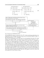
Fig. 6. Block diagram of the new ULF RFID system.
This system has been completely fabricated and tested in the laboratory (Ciudad et al., 2004)
(Ciudad Rio-Perez et al., 2008). Different geometrical arrangements for the antennas have
successfully been used. In addition, a theoretical model to develop the new RFID system for
a particular application has been developed.
3.2 Fabrication
3.2.1 Tag
The tag is formed by three different elements: i) a soft-magnetic core; ii) a low-resistance
winding; and iii) the electronics to send information.
Regarding their industrial production, the tags must be plastic or printed circuit board
(PCB)-based and the magnetic material should be obtained by electrodeposition. We have
done a PCB-based tag. Its dimensions are 5.5 cm x 8.5 cm x 1mm, like in a common credit
card. The tag is fabricated by joining two PCBs. These PCBs have some copper tracks in one
of their faces (Figure 7.A) and the magnetic material on the other (Figure 7.C). Both PCBs are
joined with the magnetic material in the inner faces. The copper lines are soldered forming a
winding all around the magnetic material (Figure 7.D). In our prototype the winding has 55
turns in the longitudinal direction.
Radio Frequency Identification Fundamentals and Applications, Design Methods and Solutions
188
Fig. 7. Photographs of the PCBs used to fabricate the tag. A and B: before the
electrodeposition of the magnetic material. C: one of the PCBs with the electrodeposited
magnetic material. D: the card after soldering the tracks of both PCBs.
Magnetic core
We have electrodeposited CoP multilayers to fabricate the magnetic core of the tag. These
multilayers are particularly useful due to their low coercivity and high permeability. CoP
monolayers exhibit perpendicular to plane magnetic anisotropy. It means that the material is
difficulty magnetized in plane. However, Co
x
P
1−x
multilayered films with different
composition within the span (0.74<x<0.86) show soft magnetic properties: i) in-plane
magnetic anisotropy; ii) low coercivity; and iii) high permeability (Perez et al., 2000).
The total thickness of the multialyer was 40 μm. It is formed by the stacking
(Co
0.74
P
0.26
/Co
0.83
P
0.17
)
N
bilayers with each layer of 20nm. This two compostions were selected
in order to have amorphous alloys covering all the substrate (Ciudad Rio-Perez et al., 2008).
(Co
0.74
P
0.26
/Co
0.83
P
0.17
)
N
multilayered amorphous films were electrodeposited on Cu
substrates under the conditions referred in (Perez et al., 2000). It was used an Autolab-
PGSTAT30 potentiostat/galvanostat to control the current density. The electrolyte was:
CoCO
3
(39.4 g/l – 0.33M), CoCl
3
.6H
2
O (181 g/l – 0.76M), H
3
PO
3
(65 g/l – 0.76M), and H
3
PO
4
(50 g/l – 0.51M). The temperature of the electrolyte during the deposition was 80 °C. It was
used a 99.9% chemical purity Co anode. The density of the electrical current needed to
deposit Co
0.74
P
0.26
was 100 mA/cm
2
whereas for Co
0.83
P
0.17
was 500 mA/cm
2
.
Electronics of the tag
In a first approach, the electronics of the tag was designed in two different modules: one for
powering and another for communications. See Figure 8. The module for powering is an
RFID in Metal Environments: An Overview on Low (LF) and Ultra-Low (ULF) Frequency Systems
189
analog multiplier circuit. Some different capacitors are charged due to the induced e.m.f in
the winding of the tag. The module for communications is formed by a microcontroller that
provides control signals (0/1) to the gate of a MOSFET. This MOSFET acts like a switch to
open and short-circuit the winding. The communication module is also similar to an analog
multiplier circuit in which some capacitors have been removed in order to improve the
response time. As microcontroller we have used a PIC16LF84A from MicroChip. It can be
powered by only 2V and it can work with only 15 μA.
Fig. 8. Initial designs for the electronics of the tag. Up: module to power the PIC. Down:
module for communications.
The inductive coupling-based RFID systems use to include a Zener diode 5V6 to protect the
circuit of the tag from high voltages when approaching it to the antenna. In our case, this
protection is not needed because the voltage is limited by the capacitors.
In a later stage, we simplified these circuits by unifying both modules as shown in Figure 9.
Fig. 9. Simplified electronics of the tag for powering and communications.
3.2.2 Reader
The reader is a tuneable magnetic field sensor. It detects the change in the magnetization of
the tag due to the switching of the winding. The magnetic sensor must be tuned at the
Radio Frequency Identification Fundamentals and Applications, Design Methods and Solutions
190
frequency of the magnetization of the tag. This frequency is that of the applied magnetic
field by the antenna.
The best option is to use a fluxgate and the double demodulation in phase technique (Aroca
et al., 1995).
Fluxgate
A fluxgate is formed by a soft magnetic core and two different windings. The primary or
excitation winding generates a magnetic field able to saturate periodically in both polarities
the magnetic core. In the secondary or pickup winding is induced an e.m.f. The amplitude of
the second harmonic of the e.m.f. in the secondary winding is proportional to any external
magnetic field. The sensitivity of the fluxgates spans in the range 10
-10
to 10
-4
T. A good
introduction to fluxgate sensors can be found in (Ripka, 2001).
We have used two different fluxgates. A common one described in (Aroca et al., 1995) and a
planar one described in (Perez et al., 2004). The last one is particularly interesting because it
is fabricated in PCB technology and its magnetic core is electrodeposited.
Double demodulation in phase
Figure 6 shows the demodulation technique used in the RFID system. All signals for
excitation and sensing are obtained from the same frequency source. The primary winding
is excited by an AC current with frequency f. A first lock-in amplifier is used to select the
second harmonic of the signal induced in the secondary winding of the fluxgate sensor
(frequency 2f). The time constant must be carefully selected so that the amplitude of the
second harmonic, as well as any change due to the presence of the tag in the surroundings,
can be measured.
If the tag is magnetized with frequency f
m
(f
m
<<f) by the applied magnetic field, the
amplitude of the signal after the first lock-in amplifier is modulated at this frequency. A
second lock-in is used to demodulate the output signal of the first lock-in amplifier. The
reference frequency for the second one is f
m
.
3.2.3 Antenna
It produces the AC magnetic field to power the tag and magnetize the magnetic material in
it. The antenna must also provide of an area in which the magnetic field is compensated.
This area is needed to place the reader avoiding its magnetic saturations due to the applied
magnetic field. Different antennas can be designed. We have successfully proved two
different geometrical arrangements.
Antenna for a standard fluxgate
The first design of the antenna was a Helmholtz pair of coils with both coils connected in
opposition. Figure 10. The fluxgate is placed centred in between the two coils. In this area
the magnetic field is zero. We have used a standard fluxgate with a 12 kHz excitation signal.
Applying an AC magnetic field of only 1 gauss of amplitude and 1.9 kHz of frequency, the
reader is able to detect the signal of the tag even through an aluminium folder and in close
contact to the tag and with a thickness up to 0.2 mm.
The magnetic field as a function of the distance for this antenna is given in (Ciudad et al.,
2004).
Antenna for a planar-type fluxgate
The antenna for the planar fluxgate is also planar. Figure 10. This antenna can be fabricated
in PCB technology. It is formed by two spiral and planar windings. They are connected to