Adaptive Techniques for Dynamic Processor Optimization_Theory and Practice Episode 1 Part 4 pdf
Bạn đang xem bản rút gọn của tài liệu. Xem và tải ngay bản đầy đủ của tài liệu tại đây (1.88 MB, 20 trang )
46 Maurice Meijer, José Pineda de Gyvez
References
[1] W. Haensch, et al., “Silicon CMOS devices beyond Scaling”, IBM Journal of
Research and Development, July/September 2006, Vol. 50, No. 4/5, pp.
339–361
[2] D.J. Frank, “Power constrained CMOS scaling limits”, IBM Journal of
Research and Development, March/May 2002, Vol. 46, No. 23, pp. 235–244
[3] AMD PowerNOW! Technology, AMD white paper, November 2000,
[4] M. Fleishman, “Longrun power management; Dynamic power management
for crusoe processor”, Transmeta white paper, January 2001,
[5] S. Gochman, et al., “The Intel Pentium M processors: Microarchitecture and
performance”, Intel Technology Journal, May 2003, Vol. 7, No. 2, pp. 22–36
[6] T. Kuroda, et al., “Variable supply-voltage scheme for low-power high-
speed CMOS digital design”, IEEE Journal of Solid-State Circuits, March
1998, Vol. 33, No. 3, pp. 454–462
[7] K. Nowka, et al., “A 32-bit PowerPC system-on-a-chip with support for
dynamic voltage scaling and dynamic frequency scaling”, IEEE Journal of
Solid-State Circuits, November 2002, Vol. 37, No. 11, pp. 1441–1447
[8] V. Gutnik and A. Chandrakasan, “Embedded power supply for low-power
DSP”, IEEE Transactions on Very Large Scale Integration (VLSI) Systems,
December 1997, Vol. 5, No. 4, pp.425–435
[9] T. Miyake, et al., “Design methodology of high performance microprocessor
using ultra-low threshold voltage CMOS”, Proceedings of IEEE Custom
Integrated Circuits Conference, 2001, pp. 275–278
[10] J. Tschanz, J. Kao, S. Narendra, R. Nair, D. Antoniadis, A. Chandrakasan,
and Vivek De, “Adaptive body bias for reducing impacts of die-to-die and
within-die parameter variations on microprocessor frequency and leakage”,
IEEE Solid-State Circuits Conference, February 2002, Vol. 1, pp. 422–478
[11] T. Chen and S. Naffziger, “Comparison of Adaptive Body Bias (ABB) and
Adaptive Supply Voltage (ASV) for improving delay and leakage under the
presence of process variation”, IEEE Transactions on VLSI Systems,
October 2003, Vol. 11, No. 5, pp. 888–899
[12] T. Sakurai and R. Newton, “Alpha-power law MOSFET model and its
applications to CMOS inverter delay and other formulas”, IEEE Journal of
Solid-State Circuits, April 1990, Vol. 25, No. 2, pp. 584–593
[13] K.Roy, S. Mukhopadhyay, and H. Mahmoodi-Meimand, ”Leakage current
mechanisms and leakage reduction techniques in deep-submicrometer
CMOS circuits ”, Proceedings of the IEEE, February 2003, Vol. 91, No. 2
pp. 305–327
[14] M. Meijer, F. Pessolano, and J. Pineda de Gyvez, “Technology exploration
for adaptive power and frequency scaling in 90nm CMOS”, Proceedings of
International Symposium on Low Power Electronic Design, August 2004,
pp.14–19
Chapter 2 Technological Boundaries of Voltage and Frequency Scaling 47
[15] M. Meijer, F. Pessolano, and J. Pineda de Gyvez, “Limits to performance
spread tuning using adaptive voltage and body biasing”, Proceedings of
International Symposium on Circuits and Systems, May 2005, pp.23–26
Chapter 3 Adaptive Circuit Technique
Tadahiro Kuroda,
1
Takayasu Sakurai
2
1
Keio University,
2
University of Tokyo
3.1 Introduction
Adaptive circuit techniques for minimizing power consumption are classi-
fied in terms of what is monitored, how it is monitored, what is controlled,
how, and in what granularity it is controlled (Figure 3.1).
As for “what is monitored”, there are two objects; one is regarding IC
operation such as speed, voltage, leakage current, and temperature. The
other object is a request to an LSI chip such as workload, quality of ser-
vice, and error rate. A replica circuit of a critical path, such as a ring oscil-
lator, is often used for monitoring the speed of an LSI chip. In monitoring
temperature of a chip, on the other hand, a temperature sensor is placed by
an actual circuit.
for Managing Power Consumption
What is controlled? Clock frequency (f), power supply voltage (V
DD
),
and threshold voltage of a transistor (V
TH
) are most common targets. The
way to control is extending from an analog approach to a digital one and a
software-assisted approach. In the digital approach, monitored information
can be stored in a register. Since software can use upper system informa-
tion, more sophisticated control is possible for further power reduction.
A. Wang, S. Naffziger (eds.), Adaptive Techniques for Dynamic Processor Optimization,
DOI: 10.1007/978-0-387-76472-6_3, © Springer Science+Business Media, LLC 2008
50 Tadahiro Kuroda, Takayasu Sakurai
Granularity of the control is another aspect. The finer the granularity in
terms of time and space, the further the power reduction, but at a cost of
increase in layout area and other associated penalties. Since power con-
sumption is becoming a serious problem, the granularity tends to be finer.
The granularity has changed timewise from a millisecond order to a micro-
second order and spatially from a chip level to a block level.
In this chapter, circuit techniques for the adaptive control are presented.
They are reviewed from perspectives of what to monitor, how to monitor,
what to control, how to control, and the granularity of the control. Adap-
tive V
DD
and V
TH
controls and cooperative control with software and oper-
ating system will be discussed in detail.
3.2 Adaptive V
DD
Control
3.2.1 Dynamic Voltage Scaling
Dynamic voltage scaling (DVS) [1] is one of the most popular approaches
in power reduction. V
DD
is dynamically lowered to an extent where re-
quired performance of the target system is ensured. Significant power re-
duction is possible with DVS, since dynamic power of CMOS circuits is
proportional to the square of V
DD
.
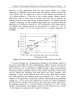
Power consumption due to leakage current is also reduced effectively by
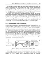
DVS in scaled devices [2], as shown in Figure 3.2. Since the subthreshold
leakage current is caused by a drain-induced barrier lowering (DIBL) ef-
fect, the lower V
DD
results in the higher V
TH
, and the smaller subthreshold
leakage current. Gate leakage current is also reduced as well.
z What to monitor
z How to monitor
z What to control
z How to control
z Granularity of control
Figure 3.1 Adaptive control classification.
Chapter 3 Adaptive Circuit Technique for Managing Power Consumption 51
Figure 3.2 Power dissipation dependence on V
DD
. Lowering V
DD
is effective in re-
ducing not only active power but also leakage power.
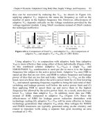
3.2.2 Frequency and Voltage Hopping
Cooperative control of both clock frequency (f) and supply voltage (V
DD
)
generates a multiplier effect in power reduction. Power consumption (P)
dependence on clock frequency in a frequency–voltage cooperative power
control (FVC) [3] differs from design to design. Figure 3.3 shows a typical
P–f curve. The P–f curve is generally expressed as [4]
fkP
'
= when
m
f
f≤ ,
γ
kfP = when
m
f
f≥ , (3.1)
where f
m
is clock frequency at the lowest power supply voltage, V
min
, and
k, k’, and γ are constants determined by design parameters. γ is larger than
1 and typically smaller than 2.5. The P–f curve is composed of two parts: a
linear region when f < f
m
, and a γ-power region when f > f
m
. In the linear
region, P is directly proportional to f, since V
DD
is constant. In the
γ
-power
region, P is proportional to the
γ
th power of f. We know through our ex-
perience that Equation (3.1) gives a good approximation in real designs.
65nm technology Node
V
TH
=0.15V, DIBL coeff.=0.2
0 0.5 1
0
0.5
1
Normalized power
V
DD
[V]
P
DYNAMIC
P
SUBTHRESHOLD LEAK
P
GATE LEAK
1
2
3
4
5
0
Normalized delay
Delay
65nm technology Node
V
TH
=0.15V, DIBL coeff.=0.2
0 0.5 1
0
0.5
1
Normalized power
V
DD
[V]
P
DYNAMIC
P
SUBTHRESHOLD LEAK
P
GATE LEAK
1
2
3
4
5
0
Normalized delay
Delay
0 0.5 1
0
0.5
1
Normalized power
V
DD
[V]
P
DYNAMIC
P
SUBTHRESHOLD LEAK
P
GATE LEAK
1
2
3
4
5
0
Normalized delay
Delay
52 Tadahiro Kuroda, Takayasu Sakurai
Figure 3.3 Power-frequency relation; (a) P–f curve in continuous DVS (solid line)
and piecewise linear relation in frequency–voltage hopping (dashed line);
(b) power waste by introducing frequency–voltage hopping.
In practical design, f and V take discrete values, since otherwise circuit
design and testing become so complicated that large associated penalties
need to be paid. Let us assume that f changes in a discrete fashion, such as
f
1
, f
2
, f
3
, and so on. Let us call this frequency change as a frequency–
voltage hopping. The P–f curve is represented by piecewise linear func-
tion, as shown by the dashed line in Figure 3.3. Figure 3.3b depicts a waste
of power dissipation, P
r
–P
i
, in the frequency–voltage hopping, compared
to the case where the clock frequency changes in a continuous fashion.
Relative value of the waste, P
r
/P
i
, for the region of f > f
m
is given by
() ( )
()
1
1
r
i
K
P
P
γ
γ
α ββα
βα
−+−
=
−
,
(3.2)
where
2
i
f
f
α
= ,
2
1
f
f
=
β
, and
1
2
m
f
K
f
γ
−
⎛⎞
=
⎜⎟
⎝⎠
.
By differentiating Equation (3.2) in terms of α and setting the result to
zero, it is found that the waste becomes the largest at
()
( )
( )
K
K
−
−−
=
−1
0
1
γ
γ
βγβ
βγ
α
(3.3)
The maximum of P
r
/P
i
is then given by substituting α
0
for α in Equation
(3.2).
Chapter 3 Adaptive Circuit Technique for Managing Power Consumption 53
If f
i
takes values uniformly from f
2
to f
1
, average of the waste, which is
given by
()
()
()
()
ri
n
ii
n
Pfn
Pfn
∑
∑
, can be approximately calculated as a ratio of area
under the dashed line as defined by trapezoid ABCD in Figure 3.3b over
area under the solid curve as depicted by hatched area. The average waste
is calculated by
()
()
()
()
()()
()
()
()()
1
122 2 1
11
1121
ri
n
ii
n
Pfn
Pfn
γ
γγ
βγηβ
γηβη βη
−
−+
−+ +
≈
+−−−
∑
∑
, (3.4)
where
η
= f
1
/f
m
.
From Equations (3.2)–(3.4), we can calculate the waste of power in in-
troducing the frequency–voltage hopping compared to the case where we
employ the continuous DVC. Table 3.1 shows the calculation results. Sup-
pose a case where f
m
= f
2
, in other words, V
DD
changes from its maximum
to minimum values accordingly as f changes from f
1
to f
2
. If f
2
is chosen
larger than half of f
1
, the average waste of power is smaller than 13%. Re-
member that
γ
is typically smaller than 2.5. Let us next suppose a case
where f
m
= (f
1
+ f
2
)/2; in other words, V
DD
changes from its maximum to
minimum values, and V
DD
stays at V
min
after f is lowered beyond f
m
. The
average waste of power is bigger than the previous case, but still it is
smaller than 20%.
From these discussions, it is concluded that in the frequency–voltage co-
operative power control, hopping in two levels of the clock frequency (f
1
and
f
2
) with the corresponding changes in V
DD
yields almost as good effect (with
over 80% efficiency) in power reduction as the continuous control. You can
remember it, as a rule of thumb, that f
2
should be chosen as half of f
1
.
The frequency and voltage hopping scheme is employed for MPEG-4
decoding in the Hitachi SH-4 CPU [4]. Table 3.2 summarizes the meas-
ured performance. From the measurement of the P–f characteristics,
γ
is
1.6. Since f
1
is 200MHz, f
2
is chosen to be 100MHz by applying the rule of
thumb. Since V
DD
reaches V
min
(=1.2V) before f reaches f
2
, no more f
i
is
needed. Therefore, there are three operational modes: a high-speed mode
at 200MHz, a low-speed mode at 100MHz, and a sleep mode. The average
of the power dissipation is reduced to 22.6% by introducing the low-power
mode and sleep mode.
54 Tadahiro Kuroda, Takayasu Sakurai
Table 3.1 Waste of power in frequency and voltage hopping, compared to the
continuous DVC; (a) when f
m
= f
2
(i.e., V
DD
changes from its maximum to mini-
mum values accordingly as f changes from f
1
to f
2
); (b) when f
m
= (f
2
+ f
1
)/2 (i.e.,
V
DD
changes from its maximum to minimum values, and V
DD
stays at V
min
after f is
lowered beyond f
m
). Upper and lower numbers in each column of the table denote
the average waste and the maximum waste, respectively.
(a) f
m
= f
2
γ
f1/f2
1.01 1.03 1.05 1.08
1.02 1.04 1.08 1.13
1.03 1.07 1.13 1.20
1.05 1.13 1.24 1.41
1.06 1.15 1.27 1.40
1.12 1.33 1.69 2.26
3.0
1.5
2.0
3.0
1.5 2.0 2.5
(b) f
m
= (f
1
+ f
2
)/2
γ
f1/f2
1.03 1.06 1.09 1.13
1.06 1.12 1.19 1.26
1.05 1.11 1.17 1.24
1.10 1.22 1.36 1.52
1.09 1.18 1.28 1.39
1.17 1.38 1.63 1.94
3.0
1.5
2.0
3.0
1.5 2.0 2.5
Table 3.2 Experimental results of frequency and voltage hopping for MPEG-4
decoding in the Hitachi SH-4 CPU. Average power dissipation was
reduced to 22.6%.
Operation mode High speed Low speed Sleep
Voltage (V) 2.0 1.2 1.2
Frequency (MHz) 200 100 0
Power (mW) 600 200 20
Execution time (%) 3.3 53.5 43.2
Average power
135.6 (22.6% of the power in HS mode)
Chapter 3 Adaptive Circuit Technique for Managing Power Consumption 55
3.3 Adaptive V
TH
Control
Delay variation (ΔT
pd
) due to V
TH
variation (ΔV
TH
) is substantially in-
creased at low V
DD
’s. The increased variation of the gate propagation delay
degrades the chip performance. In order to keep the delay variation per-
centage constant in low V
DD
’s, ΔV
TH
should be reduced approximately by
[5]
α
1
'
'
'
⎟
⎟
⎠
⎞
⎜
⎜
⎝
⎛
⋅=
Δ
Δ
DD
DD
pd
pd
TH
TH
V
V
T
T
V
V
, (3.5)
where α represents the velocity saturation effect and typically is 1.3 [6],
and T
pd
is
CMOS gate propagation delay. For example, when V
DD
is lowered
from 1.5V to 1.0V and V
TH
is lowered to maintain circuit speed (i.e.,
T
pd
=T
pd
’), ΔV
TH
should be reduced by 27%. It is very difficult, however, to
lower ΔV
TH
by this much by means of process and device refinement. In
this section, circuit techniques for adapting V
TH
control are discussed.
3.3.1 Reverse Body Bias (VTCMOS)
A variable threshold voltage CMOS technology (VTCMOS) [5, 7–11]
controls V
TH
by means of substrate bias control. In this technique, devices
are fabricated for lower V
TH
than a design target, and V
TH
is set to the target
by adjusting reverse body bias (RBB), V
BB
. Since subthreshold leakage
current depends very strongly on V
TH
, V
TH
can be compensated for varia-
tions by feedback control of V
BB
such that monitored leakage current is set
to a target value.
3.3.1.1 Self-Adjusting Threshold Voltage (SAT) Scheme
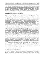
A self-adjusting threshold voltage (SAT) scheme, depicted in Figure 3.4,
compensates for the V
TH
variation [6, 7]. The subthreshold leakage current
is monitored by a leakage current monitor (LCM). The substrate bias is
generated by a self-substrate bias circuit (SSB). LCM activates SSB when
a monitored leakage current in LCM, I
leak.LCM
, is larger than a target preset
value, I
ref
. SSB lowers V
BB
by pumping out current from the substrate [12].
Accordingly, V
TH
is raised and I
leak.LCM
is reduced.
56 Tadahiro Kuroda, Takayasu Sakurai
Figure 3.4 Self-adjusting threshold voltage (SAT) scheme.
When I
leak.LCM
becomes smaller than I
ref
, LCM stops SSB. However, the
substrate current due to the impact ionization and the junction leakage
raises V
BB
gradually again. Accordingly, V
TH
is lowered gradually and
I
leak.LCM
increases. When I
leak.LCM
becomes larger than I
ref
, LCM activates
SSB again. By activating SSB intermittently in this way, V
TH
can be set to
the target value, and consequently, its process-induced variation can be
compensated to be smaller.
3.3.1.2 Leakage Current Monitor
In Figure 3.4, the ratio of I
leak.LCM
to the total leakage current in a chip,
I
leak.chip
, is given by
()
S
V
chip
LCM
SV
chip
SVV
LCM
chipleak
LCMleak
LCM
v
TH
THb
W
W
W
W
I
I
X
10
10
.
.
⋅==≡
−
−
, (3.6)
where W
chip
is effective total channel width corresponding to the total leak-
age current in the chip, W
LCM
is channel width of a monitor transistor in
LCM, S is the subthreshold slope, and V
b
is its gate potential. Since I
leak.LCM
leads to a power penalty of LCM, it should be as small as possible. Too
small I
leak.LCM
, however, slows LCM response speed, which enlarges fluc-
tuation of V
BB
caused by the on–off control of SSB, resulting in larger dy-
namic error of V
TH
. When I
leak.LCM
is 1μA for the chip leakage current of
1mA, the leakage current detection ratio, X
LCM
, is 0.1%. Given V
b
=2S,
which is approximately 0.2V, the size of the monitor transistor can be
p-well
I
leak.LCM
V
b
W
LCM
Leakage Current Monitor
(LCM)
"L"
I
leak.chip
chip
W
chip
I
ref
W
1
W
2
on / off
Self-Substrate Bias
(SSB)
M
1
p-well
I
leak.LCM
V
b
W
LCM
Leakage Current Monitor
(LCM)
"L"
I
leak.chip
chip
W
chip
I
ref
W
1
W
2
on / offon / off
Self-Substrate Bias
(SSB)
M
1
Chapter 3 Adaptive Circuit Technique for Managing Power Consumption 57
designed as small as approximately 0.001% of the effective total transis-
tors in the chip.
A bias circuit for V
b
is depicted in Figure 3.4. A current source is de-
signed such that the two transistors are operated in the subthreshold region.
As the drain currents of the two transistors are equal,
SVV
SVVV
TH
THb
WW
/)(
1
/)(
2
1
1
1010
−
−−
⋅=⋅ ,
1
2
log
W
W
sV
b
⋅=∴ . (3.7)
Substituting Equation (3.7) into Equation (3.6),
1
2
W
W
W
W
X
chip
LCM
LCM
⋅= . (3.8)
X
LCM
can be determined only by transistor size ratio and independent of
V
DD
, temperature, and process variation. If V
b
is generated by dividing
voltages between V
DD
and V
SS
by resistors (V
b
= λ V
DD
), and consequently,
X
LCM
is a function of V
DD
and S. Since S is a function of temperature, X
LCM
depends on V
DD
and temperature, which is not desirable. Variation in X
LCM
,
analyzed by SPICE simulation, is within 15%, which results in less than
1% error in V
TH
controllability.
3.3.1.3 V
TH
Controllability
An MPEG-4 video codec chip [13] is fabricated in two runs. The target of
V
TH
in one run is 0.05V and that for the other is 0.15V by changing condi-
tions of ion implantation. About 40 chips are measured for each V
TH
condi-
tion in the following three ways: (1) V
TH
as processed without body bias-
ing, (2) V
TH
controlled by VTCMOS in the active mode, and (3) V
TH
controlled by VTCMOS in the standby mode. In (2), the MPEG-4 chip is
operated with test vector inputs so that the measurements include dynamic
errors, such as those due to substrate noise influence. The measured results
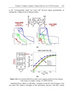
at 27°C and 70°C are plotted in Figure 3.5a–d. Statistics of the distribution
such as the average (x) and the standard deviation (σ) are presented in
Tables 3.3a and b. The VTCMOS technology reduces V
TH
variation from
±0.1V to ±0.05V in both the active and the standby modes and raises V
TH
by 0.25V in the standby mode.
58 Tadahiro Kuroda, Takayasu Sakurai
Table 3.3a Measured V
TH
as processed.
V
TH.p
(V) V
TH.n
(V)
Standby mode 27°C 70°C 27°C 70°C
Target V
TH
x
σ
x
σ
x
σ
x
σ
0.05 –0.06 0.014 0.03 0.016 0.09 0.022 0.03 0.028
0.15 –0.13 0.022 –0.05 0.021 0.16 0.029 0.11 0.031
x
: average, σ: standard deviation.
Table 3.3b Measured V
TH
controlled by VTCMOS technology.
V
TH.p
(V) V
TH.n
(V)
27°C 70°C 27°C 70°C
VTCMOS
x
σ
x
σ
x
σ
x
σ
Active mode –0.17 0.018 –0.20 0.016 0.25 0.019 0.28 0.019
Standby mode –0.44 0.015 –0.47 0.016 0.46 0.019 0.48 0.036
x
: average, σ: standard deviation.
Figure 3.5 Measured V
TH.
: (a) V
TH.p
at 27°C, (b) V
TH.p
at 70°C, (c) V
TH.n
at 27°C,
and (d)
V
TH.n
at 70°C.
Chapter 3 Adaptive Circuit Technique for Managing Power Consumption 59
Figure 3.6
Measured chip leakage current.
Measured temperature dependence of V
TH
is 0.7mV/°C for an NMOS
and –0.7mV/°C for a PMOS under the VTCMOS control, whereas the
values in the conventional CMOS device are –1.3mV/°C and 2.0mV/°C,
respectively. When V
DD
is around 0.5V, the drain current shows positive
temperature dependence, since the increase in the drain current by V
TH
de-
crease surmounts the mobility degradation [14]. This may cause thermal
runaway if the subthreshold leakage becomes the dominant component in
power dissipation at low V
TH
. In a scaled device with low V
DD
and low V
TH
,
temperature dependence control becomes indispensable. The temperature
dependence of V
TH
in VTCMOS can be controlled by controlling the tem-
perature dependence of I
ref
in LCM.
Chip leakage current is measured at 27°C and 70°C, and the results are
plotted in Figure 3.6. The horizontal axes is the average of |V
TH.p
|+V
TH.n
.
The VTCMOS technology sets the leakage current below 10mA in the ac-
tive mode and below 10μA in the standby mode, independently from proc-
essed V
TH
and temperature.
3.3.1.4 Device Perspective
In applying RBB, the drain-substrate depletion layer extends, which wors-
ens the short-channel effect (SCE) and the V
TH
variations across a die. Fur-
thermore, the body effect coefficient, γ, is reduced more in a shorter chan-
nel transistor, since channel potential is more influenced by drain than by
substrate due to the DIBL effect. Coupled with SCE, the V
TH
variation
across a die is increased by the substrate bias. Measurement in 0.18μm
single-V
TH
and 0.13μm dual-V
TH
logic technologies for high-performance
microprocessors shows that [15] (1) RBB becomes less effective for leak-
age reduction at shorter channel lengths and lowers V
TH
at both high and
60 Tadahiro Kuroda, Takayasu Sakurai
room temperatures when leakage currents are large and (2) RBB effective-
ness also diminishes with technology scaling primarily because of worsen-
ing SCE, especially when the target V
TH
value is low.
The simplified scaling theory predicts that it will eventually be difficult
to cause a large-enough change in V
TH
through RBB. In practice, however,
RBB is still effective in the 65nm technology generation by careful chan-
nel engineering and V
DD
control [16].
3.3.2 Forward Body Bias
From the observations on device scaling in the previous section, the range
of substrate biasing is extended from RBB to forward body bias (FBB)
[17]–[19]. FBB is applied to a transistor with high V
TH
to bring V
TH
down
to the target value.
Since FBB improves the device short-channel effects, it reduces sensi-
tivity of V
TH
to variation in gate length, oxide thickness, and channel dop-
ing. As a result, it is reported in [19] that die-to-die V
TH
variation is 36%
smaller in a PMOS and 48% smaller in an NMOS when FBB is used, even
with ±20% variation in the body bias value.
Even though FBB lowers V
TH
and improves circuit performance, FBB
increases leakage current due to parasitic bipolar current and forward
source–body junction current. This determines an optimum FBB value.
The optimum FBB value, between 400 and 500mV at 110°C, provides
maximum frequency improvement (13%). The total switched capacitance
and switching energy are 10% higher because of larger junction capaci-
tance, larger average gate capacitance at lower V
TH
, and increased short-
circuit current. Although active leakage power, including subthreshold
leakage, parasitic bipolar current, and forward source–body junction cur-
rent, increases by 10–100×, it remains sufficiently small compared to
switching power. For bias values larger than this optimum, junction ca-
pacitance, body effect, and source–body junction forward current in-
crease rapidly and fully negate any delay improvements induced by fur-
ther V
TH
reduction. Active leakage power also becomes an unacceptably
large fraction of the total power. For designs operating at a maximum
junction temperature of 110°C, the desired FBB value is 450mV with
±50mV tolerance.
Chapter 3 Adaptive Circuit Technique for Managing Power Consumption 61
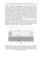
Figure 3.7 MPEG-4 video codec chip with VTCMOS technology. Leakage cur-
rent is monitored by a replica circuit. RBB is applied by analog control in granu-
larity of a chip level and a millisecond order.
3.3.3 Control Method and Granularity
As one of the early examples where the VTCMOS technology was em-
ployed, Figure 3.7 shows a microphotograph of an MPEG-4 video codec
chip that was presented in 1998 [13]. The chip was fabricated in a 0.3μm
CMOS n-well/p-sub technology. Three million transistors are integrated on
the chip, including a 52-kB SRAM. The chip size is 9mm by 9mm. Leak-
age current is monitored by using a replica circuit in Figure 3.4. RBB is
applied by an analog control in granularity of a chip level and a millisec-
ond order.
The monitor objects have been extended from leakage current to speed,
the voltage ranges of substrate biasing from RBB to forward body bias
(FBB), and the control method from analog to digital.
Figure 3.8 shows a microphotograph of a microprocessor with a speed-
adaptive threshold voltage (SA-Vt) CMOS scheme [20]. The chip was fab-
ricated in a 0.2μm CMOS triple-well technology. The body bias is con-
tinuously controlled from –1.5V (RBB) to +0.5V (FBB) by digital control
to compensate for fluctuations in fabrication and changes in V
DD
and oper-
ating temperature.
Since circuit speed depends on both a PMOS V
TH
and an NMOS V
TH
,
they cannot be determined uniquely by monitoring only speed. As shown
in Figure 3.9, logical threshold voltage of a CMOS gate is also monitored
to keep it for a prefixed value. Both V
TH
’s of PMOS and NMOS can be
uniquely determined [21].
62 Tadahiro Kuroda, Takayasu Sakurai
Figure 3.8
Microprocessor chip and speed-adaptive threshold voltage (SA-Vt)
CMOS scheme. Speed is monitored by a replica circuit. Body bias is extended
from RBB to FBB and controlled by digital in granularity of a chip level and a
millisecond order.
P-/3SUBSTRATEBIAS
#LOCKSIGNAL
$ELAYLINE
N-/3SUBSTRATEBIAS
3WITCHCONTROLSIGNAL
n6
n6
6
6SS
6DD
6
)NTEGRATED
#IRCUITS
6BP
6BN
!MPLIFIER
!MPLIFIER
6
6
6
6
6
6
STBY
STBY
$ECODER
#OMPARATOR
3WITCHCONTROLSIGNAL
Chapter 3 Adaptive Circuit Technique for Managing Power Consumption 63
Figure 3.9 Logical threshold monitor.
Figure 3.10 Microphotograph of sub-site and block diagram of adaptive
body bias circuit.
Granularity of control in terms of space and time is becoming finer;
from chip to block levels [22], and from microsecond to nanosecond
ranges [23]. For instance, in Figure 3.10, body of a chip is biased separately
64 Tadahiro Kuroda, Takayasu Sakurai
A self-adjusted forward body bias (SAFBB) scheme [23] in Figure 3.11
is employed for gated body. The total current for generating FBB is limited
by a current source in a controller such that the DC current does not domi-
nate the total current dissipation, independent of the number of transistors
in a block under the FBB control. The chip was fabricated in a 0.13μm
CMOS p-substrate twin-well technology. FBB is applied by analog control
in granularity of a block level. The body bias for PMOS changes within
1μs. Such a short changing time is possible because of two reasons; the
current source continues to charge the body until body voltage reaches its
final value for FBB, and the sub-site is as small as a block.
Figure 3.11 Self-adjusted forward body bias (SAFBB) scheme and
body waveforms.
3.3.4 V
TH
Control Under Variations
Although the spatial granularity of the body biasing will be finer, it shall
be very difficult to control each V
TH
transistor by transistor. Still the adap-
tive V
TH
control shall keep its effectiveness with the following reason.
in 21 sub-sites that are distributed over 4.5mm by 6.7mm [22]. The chip
was fabricated in a 0.15μm CMOS technology. N-well for PMOS is con-
tinuously controlled from –0.5V (RBB) to +0.5V (FBB) by digital control.
Each sub-site has a replica of the critical path whose delay is compared
against an externally applied target clock frequency.
Chapter 3 Adaptive Circuit Technique for Managing Power Consumption 65
Suppose a circuit with many transistors whose V
TH
’s receive random
variation, and the variation is expressed by the normal distribution as
shown in Figure 3.12, with average value, V
TH0
, and standard deviation,
σ
VTH
.
Figure 3.12 Random variation of V
TH
and I
leak
.
Average of subthreshold leakage current is given by [24]
()()
∫
∞
∞−
=
THTHTHleakleak
dVVfVII
()
∫
∞
∞−
−
−
−
=
TH
VV
VTH
S
V
leak
dVeeI
VTH
THTH
TH
2
2
0
2
10ln
0
2
1
σ
σπ
S
leak
S
leak
VTH
VTH
IeI
2
10ln
0
2
10ln
0
2
2
10
σ
σ
==
⎟
⎠
⎞
⎜
⎝
⎛
, (3.9)
where I
leak0
is leakage current at V
TH0
. Corresponding average V
TH
that
yields <I
leak
> is given by
S
VV
VTHTHTH
2
10ln
2
0
σ
−=
(3.10)
The relation in Equation (3.10) is plotted in Figure 3.13. The figure
shows that even if V
TH
fluctuates randomly by σ
VTH
of 30mV, average of
the total leakage of a circuit increases only by the equivalent amount when
V
TH
is lowered only by 10mV. In other words, random fluctuation of V
TH
in
each transistor does not bring a significant impact in leakage current of the
circuit. This sounds quite natural if you notice a fact that a transistor with
V
TH
lowered by 3σ
VTH
has around 10 times larger leakage current, but since
such a transistor exists only at a rate of 1.5 per 1000 transistors, it brings
s
V
leakleak
TH
eII
10ln
0
−
=
V
GS
[V]
log(I
DS
) [A/μm]
I
leak0
VTH
σ
leak
σ
V
TH0
0
average : <V
TH
>
average: <I
leak
>
s
V
leakleak
TH
eII
10ln
0
−
=
V
GS
[V]
log(I
DS
) [A/μm]
I
leak0
VTH
σ
leak
σ
V
TH0
0
average : <V
TH
>
average: <I
leak
>
66 Tadahiro Kuroda, Takayasu Sakurai
small impact to the total leakage current. Random fluctuation in V
TH
brings
less impact on leakage current of a circuit than inter-chip V
TH
fluctuations
that can be compensated effectively by the adaptive V
TH
control. Adaptive
control to compensate for fluctuations in transistor level is not needed.
The same effect of statistical distribution can be found in a path delay.
For instance, delay time of a path that is composed of n-stage gates is
given as sum total of delay time of the n gates. Suppose delay time of each
gate receives random variation of the Gaussian distribution, relative varia-
tion of the path delay is reduced to
n1
of that of the gate delay, accord-
ing to the central limit theorem. Speed variation caused by random V
TH
variation becomes smaller as n increases.
Figure 3.13 Average leakage dependence on V
TH
variation.
On the other hand, if V
TH
varies in clusters, lot by lot, chip by chip, or
block by block, it brings large impact on circuit speed and leakage current
because all V
TH
’s are shifted to the same direction. These systematic varia-
tions can be reduced effectively by the adaptive V
TH
control.
3.3.5 V
TH
Control vs. V
DD
Control
Variations in path delay can be compensated by the adaptive control of V
TH
and/or V
DD
. Which control is more efficient?
Power dissipation of a CMOS circuit is given by
S
V
DDDDleakdynamictotal
TH
WIVfCVPPP
−
+=+= 10
0
2
α
(3.11)
Standard deviation of V
TH
σ
VTH
[mV]
Equivalent V
TH
shift
<V
TH
> - V
TH0
[mV]
0 10 20 30 40 50
0
20
60
100
140
3σ
S=80
S=100
S
VV
VTHTHTH
2
10ln
2
0
σ
−=−><
Standard deviation of V
TH
σ
VTH
[mV]
Equivalent V
TH
shift
<V
TH
> - V
TH0
[mV]
0 10 20 30 40 50
0
20
60
100
140
3σ
S=80
S=100
Standard deviation of V
TH
σ
VTH
[mV]
Equivalent V
TH
shift
<V
TH
> - V
TH0
[mV]
0 10 20 30 40 50
0
20
60
100
140
3σ
S=80
S=100
S
VV
VTHTHTH
2
10ln
2
0
σ
−=−><