Adaptive Techniques for Dynamic Processor Optimization_Theory and Practice Episode 1 Part 4 potx
Bạn đang xem bản rút gọn của tài liệu. Xem và tải ngay bản đầy đủ của tài liệu tại đây (968.81 KB, 20 trang )
Chapter 3 Adaptive Circuit Technique for Managing Power Consumption 67
Let us suppose V
TH
and V
DD
are changed, while other parameters are con-
stant. The power dissipation becomes the largest (P
total.max
) under the maxi-
mum V
DD
and minimum V
TH
. A ratio of P
total
over P
total.max
is given by
()
max.
2
max.max.
min.
101
DD
DD
S
VV
L
DD
DD
L
total
total
V
V
V
V
P
P
THTH
−
+
⎟
⎟
⎠
⎞
⎜
⎜
⎝
⎛
−=
ηη
, (3.12)
where
η
L
is a ratio of leakage power to the total power dissipation.
max.
max.
total
leak
L
P
P
=
η
(3.13)
It is known that P
total
becomes minimum at around
η
L
=0.3 when V
TH
and
V
DD
are lowered such that circuit speed is unchanged [25].
The same kind of equation for circuit speed is similarly derived and
given by
α
⎟
⎟
⎠
⎞
⎜
⎜
⎝
⎛
−
−
⎟
⎟
⎠
⎞
⎜
⎜
⎝
⎛
=
THDD
THDD
DD
DD
VV
VV
V
V
Speed
Speed
min.max.
max.
max
1
, (3.14)
where α represents the velocity saturation effect [6].
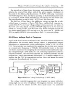
Now let us suppose a case where V
TH
is lower by 0.1V than a target
value due to process fluctuation. Circuit speed becomes 20% faster, while
Figure 3.14 Comparison between V
TH
control and V
DD
control. The V
TH
control,
compared to the V
DD
control, lowers power dissipation to half for the same circuit
speed or increases circuit speed by 20% for the same power dissipation.
Changing V
TH
0.8 0.9 1 1.1 1.2
0
1
2
3
4
5
6
Changing V
DD
V
DDH
=0.9V V
THL
=0.2V
s=80mV/decade ΔV
TH
=-0.1V
η=0.3
Speed normalized by target
Power normalized by target
power down
to 1/2
20% speed up
Changing V
TH
0.8 0.9 1 1.1 1.2
0
1
2
3
4
5
6
Changing V
DD
V
DDH
=0.9V V
THL
=0.2V
s=80mV/decade ΔV
TH
=-0.1V
η=0.3
Speed normalized by target
Power normalized by target
power down
to 1/2
20% speed up
68 Tadahiro Kuroda, Takayasu Sakurai
power dissipation becomes six times larger. Let us next apply the adaptive
V
TH
control and the adaptive V
DD
control. The calculation results by using
the above equations are plotted in Figure 3.14. When V
TH
is raised by the
adaptive V
TH
control, power dissipation is lowered to half compared to the
case where V
DD
is lowered by the V
DD
control. When V
TH
is lowered, cir-
cuit speed is increased by 20% compared to the case where V
DD
is raised.
The adaptive V
TH
scheme works more effectively to compensate for varia-
tions in power and speed that are caused by fluctuations in V
TH
.
3.4 Hardware and Software Cooperative Control
The control method is extended from analog to digital and from hardware
to software. In this section, hardware–software cooperative control is pre-
sented.
3.4.1 Cooperation Between Hardware and Application Software
In real-time systems, utilization of a processor is frequently less than one,
even if all tasks run at their worst-case execution time (WCET). There is
always some slack time (worst-case slack time). Moreover, workload of
each task may vary from time to time, which results in another kind of
slack time (workload-variation slack time).
A run-time voltage hopping (RVH) scheme [26] exploits both the worst-
case slack time and the workload-variation slack time. Clock frequency
(f
CLK
) and hence supply voltage (V
DD
) are scheduled as depicted in Figure
3.15 with the following steps.
(1) A task is divided into N timeslots. Following parameters are obtained
through static analysis or direct measurement; WCET of whole task
(T
WC
), ith timeslot (T
WCi
), and WCET from (i+1)th to Nth timeslots
(T
Ri
).
(2) For each timeslot, target execution time (T
TAR
) is calculated as T
TAR
=
T
WC
– T
WCi
– T
ACC
– T
TD
, where T
ACC
is accumulated execution time
from 1st to (i–1)th timeslots, and T
TD
is transition delay to change f
CLK
and V
DD
.
(3) For each candidate clock frequency, f
j
=f
CLK
/j (j=1, 2, 3…), estimated
maximum execution time Tj is calculated as T
j
= T
Wi
*j. If f
j
is not equal
to clock frequency of (i–1)th timeslot, T
j
= T
j
+ T
TD
.
Chapter 3 Adaptive Circuit Technique for Managing Power Consumption 69
Figure 3.15
f
CLK
and V
DD
scheduling in RVH scheme.
Figure 3.16 Power reduction of MPEF-4 encoding by RVH scheme.
(4) Clock frequency f
VAR
is determined as minimum clock frequency f
j
whose estimated maximum execution time T
j
does not exceed target
time T
TAR
, as shown in Figure 3.15.
(5) Supply voltage V
VAR
is determined from the lookup table.
Steps (1) and (2) are performed at compile, while steps (3)–(5) are carried
out at run time.
Figure 3.16 shows measured power dissipation reduction ratio when the
scheme is employed to an MPEG-4 SP@L1 video encoding application. It
is seen that power dissipation is reduced to 6%. Only two discrete levels of
clock frequency (f, f/2) are sufficient, meaning that the scheme is very
simple in both hardware and software designs.
70 Tadahiro Kuroda, Takayasu Sakurai
3.4.2 Cooperation Between Hardware and Operating System
The RVH scheme is limited to a single application. A cooperative power
optimization method among operation system (OS), applications, and
hardware platform is essential [27, 28]. Cooperation is needed because OS
only knows global timing information among tasks, while each application
has knowledge about its own structure and behavior.
Figure 3.17 Scheduling; (a) task set, (b) conventional rate-monotonic
scheduling, (c) slice-level control of speed without interaction with OS, (d) coop-
erative scheduling.
OS controls the execution flow of tasks with off-the-shelf microproces-
sor and custom chips that provide power-down mode and discrete levels of
speed (i.e., f and V
DD
). The main function of OS consists of (1) providing
virtual deadline to each task in such a way that deadlines of all tasks are
always guaranteed and (2) predicting the exact time interval during which
there is no activity on the processor and bringing the processor into power
down. This is done based on status of queues (ready queue and dominant
queue).
An example is shown in Figure 3.17 [27]. Consider the two tasks shown
in Figure 3.17a. Suppose that they consist of four and six slices, respec-
tively, with each slice requesting 2 time units for its WCET. If we assume
that period is equal to deadline, rate monotonic priority assignment is a
natural choice meaning that A gets higher priority. A typical schedule,
when each slice runs at half of its WCET, is shown in Figure 3.17b. Sup-
pose that there are three speed levels; 1, 1/2, and 1/3. The cooperative
scheduling is shown in Figure 3.17d. At time 0, A is forced to complete its
execution within its WCET at 8 because B is in RUN state. This is similar
to having virtual deadline at 8. At time 6, A goes to DORMANT state.
Thus, the virtual deadline of B is set to 20, which is the minimum of its
Chapter 3 Adaptive Circuit Technique for Managing Power Consumption 71
deadline at 30 and the next arrival time of A at 20. The remaining schedule
can be verified similarly. For comparison, Figure 3.17c shows a schedule
when the method in [26] is applied to a multitasking environment if proper
support from OS is possible.
Experimental results with a prototype system in [28] show that 74%
power saving is possible in multitask multimedia environment compared to
the conventional real-time OS (μITRON) when workload is 38%.
3.5 Conclusion
Adaptive circuit techniques for reducing power consumption are presented
from perspectives of what to monitor, how to monitor, what to control,
how to control, and the granularity of the control.
The monitor object is extended from leakage current to speed, voltage,
and temperature. Replica circuits such as a leakage current monitor, a ring
oscillator, and a logical threshold monitor are used.
The control objects are clock frequency, V
DD
, and V
TH
. In the frequency–
voltage cooperative control, hopping in two levels of the clock frequency
(f
1
and f
2
) with corresponding changes in V
DD
yields almost as good effect
in power reduction as their continuous control. f
2
should be set at half of f
1
.
V
TH
can be controlled by body bias (VTCMOS). V
TH
variations can be
compensated by feedback control of the body bias such that monitored
leakage current is set to a target value. The range of the body biasing is ex-
tended from reverse body bias to forward body bias. The adaptive V
TH
con-
trol continues to work effectively under random variation of V
TH
in scaled
devices.
The control method is extended from analog to digital and from hard-
ware to software. The granularity of the control in terms of space and time
is becoming finer, from chip to block levels and from microsecond to
nanosecond ranges.
References
[1] T. Kuroda, K. Suzuki, S. Mita, T. Fujita, F. Yamane, F. Sano, A. Chiba,
Y. Watanabe, K. Matsuda, T. Maeda, T. Sakurai, and T. Furuyama, “Vari-
able supply-voltage scheme for low-power high-speed CMOS digital de-
sign,” IEEE J. Solid-State Circuits, vol. 33, no. 3, pp. 454–462, Mar. 1998.
[2] T. Sakurai, “Low power digital circuit design (keynote),” ESSCIRC'04, pp.
11–18, Sept. 2004. T. Sakurai, “Perspectives of low-power VLSI's,” IEICE
Transactions on Electronics, vol. E87-C, no. 4, pp. 429–437, Apr. 2004.
72 Tadahiro Kuroda, Takayasu Sakurai
[3]
A. Chandrakasan, V. Gutnik, and T. Xanthopoulos, “Data driven signal
processing: an approach for energy efficient computing,” Proc. ISLPED’96,
pp. 347–352, Aug. 1996.
[4]
K. Aisaka, T. Aritsuka, S. Misaka, K. Toyama, K. Uchiyam, K. Ishibashi,
H. Kawaguchi, and T. Sakurai, “Design rule for frequency-voltage coopera-
tive power control and its application to an MPEG-4 decoder,” Symp. on
VLSI Circuits Digest of Technical Papers, pp. 216–217, Jun. 2002.
[5] T. Kuroda, T. Fujita, S. Mita, T. Nagamatu, S. Yoshioka, K. Suzuki, F. Sano,
M. Norishima, M. Murota, M. Kako, M. Kinugawa, M. Kakumu, and
T. Sakurai, “A 0.9V 150MHz 10mW 4mm
2
2-D discrete cosine transform
core processor with variable-threshold-voltage scheme,” IEEE J. Solid-State
Circuits, vol. 31, no. 11, pp. 1770–1779, Nov. 1996.
[6]
T. Sakurai and A. R. Newton, “Alpha-power law MOSFET model and its
applications to CMOS inverter delay and other formulas,” IEEE J. Solid-
State Circuits, vol. 25, no. 2, pp. 584
–594, Apr. 1990.
[7]
T. Kobayashi and T. Sakurai, “Self-adjusting threshold-voltage scheme
(SATS) for low-voltage high-speed operation,” Proc. CICC’94, pp. 271–274,
May 1994.
[8]
K. Seta, H. Hara, T. Kuroda, M. Kakumu, and T. Sakurai, “50% active-
power saving without speed degradation using standby power reduction
(SPR) circuit,” ISSCC Dig. Tech. Papers, pp. 318–319, Feb. 1995.
[9]
T. Kuroda, T. Fujita, T. Nagamatu, S. Yoshioka, T. Sei, K. Matsuo,
Y. Hamura, T. Mori, M. Murota, M. Kakumu, and T. Sakurai, “A high-speed
low-power 0.3
μm CMOS gate array with variable threshold voltage (VT)
scheme,” Proc. CICC’96, pp. 53–56, May 1996.
[10] T. Kuroda, T. Fujita, S. Mita, T. Mori, K. Matsuo, M. Kakumu, and
T. Sakurai, “Substrate noise influence on circuit performance in variable
threshold-voltage scheme,” Proc. ISLPED’96, pp. 309–312, Aug. 1996.
[11]
T. Kuroda and T. Sakurai, “Threshold-voltage control schemes through sub-
strate-bias for low-power high-speed CMOS LSI design,” J. VLSI Signal
Processing Systems, Kluwer Academic Publishers, vol. 13, no. 2/3, pp.
191–201, Aug./Sep. 1996.
[12] R. D. Pashley and G. A. McCormick, “A 70-ns 1K MOS RAM,” ISSCC Dig.
Tech. Papers, pp. 138–139, Feb. 1976.
[13] M. Takahashi, M. Hamada, T. Nishikawa, H. Arakida, Y. Tsuboi, T. Fujita,
F. Hatori, S. Mita, K. Suzuki, A. Chiba, T. Terasawa, F. Sano, Y. Watanabe,
H. Momose, K. Usami, M. Igarashi, T. Ishikawa, M. Kanazawa, T. Kuroda,
and T. Furuyama, “A 60mW MPEG4 video codec using clustered voltage
scaling with variable supply-voltage scheme,” ISSCC Dig. Tech. Papers, pp.
34–35, Feb. 1998.
[14] K. Kanda, K. Nose, H. Kawaguchi, and T. Sakurai, “Design impact of posi-
tive temperature dependence of drain current in sub 1V CMOS VLSI’s,”
Proc. CICC’99, pp. 563–566, May 1999.
[15]
A. Keshavarzi, S. Ma, S. Narendra, B. Bloechel, K. Mistry, T. Ghani, S.
Borkar, and V. De, “Effectiveness of reverse body bias for leakage control in
scaled dual Vt CMOS ICs,” Proc. LPED’01, pp. 207–212, Aug. 2001.
Chapter 3 Adaptive Circuit Technique for Managing Power Consumption 73
[16]
M. Togo, T. Fukai, Y. Nakahara, S. Koyama, M. Makabe, E. Hasegawa,
M. Nagase, T. Matsuda, K. Sakamoto, S. Fujiwara, Y. Goto, T. Yamamoto,
T. Mogami, M. Ikeda, Y. Yamagata, and K. Imai, “Power-aware 65nm node
CMOS technology using variable V
DD
and back-bias control with reliability
consideration for back-bias mode,” Symp. on VLSI Technology Dig. Tech.
Papers, pp. 88–89, June 2004.
[17]
S. Narendra, M. Haycock, V. Govindarajulu, V. Erraguntla, H. Wilson, S.
Vangal, A. Pangal, E. Seligman, R. Nair, A. Keshavarzi, B. Bloechel, G.
Dermer, R. Mooney, N. Borkar, S. Borkar, and V. De, “1.1 V 1 GHz com-
munications router with on-chip body bias in 150 nm CMOS,” ISSCC Dig.
Tech. Papers, pp. 270–271, Feb. 2002.
[18]
S. Vangal, M. A. Anders, N. Borkar, E. Seligman, V. Govindarajulu, V. Er-
raguntla, H. Wilson, A. Pangal, V. Veeramachaneni, J. Tschanz, Y. Ye, D.
Somasekhar, B. Bloechel, G. Dermer, R. K. Krishnamurthy, K. Soumyanath,
S. Mathew, S. Narendra, M. Stan, S. Thompson, V. De, and S. Borkar,
“5-GHz 32-bit integer execution core in 130-nm dual-V/sub T/ CMOS,”
IEEE J. Solid-State Circuits, vol. 37, no. 11, pp. 1421–1432, Nov. 2002.
[19] S. Narendra, A. Keshavarzi, B. A. Bloechel, S. Borkar, and V. De, “Forward
body bias for microprocessors in 130-nm technology generation and be-
yond,” IEEE J. Solid-State Circuits, vol. 38, no. 5, pp. 696–701, May 2003.
[20]
M. Miyazaki, G. Ono, T. Hattori, K. Shiozawa, K. Uchiyama, and K. Ishi-
bashi, “A 1000-MIPS/W microprocessor using speed-adaptive threshold-
voltage CMOS with forward bias,” ISSCC Dig. Tech. Papers, pp. 420–421,
Feb. 2000.
[21]
G. Ono and M. Miyazaki, “Threshold-voltage balance for minimum supply
operation,” Symp. VLSI Circuits Dig. 16, pp. 206–209, June 2002.
[22]
J. Tschanz, J. Kao, S. Narendra, R. Nair, D. Antonladls, A. Chandrakasan,
and V. De, “Adaptive body bias for reducing impacts of doe-to-deiand
within-die parameter variations on microprocessor frequency and leakage,”
IEEE J. Solid-State Circuits, vol. 37, no. 11, pp. 1396–1402, Nov. 2002.
[23] K. Ishibashi, T. Yamashita, Y. Arima, I. Minematsu, and T. Fujimoto, “A
9
μW 50MHz 32b adder using a self-adjusted forward body bias in SoCs,”
ISSCC Dig. Tech. Papers, pp. 116
–117, Feb. 2003.
[24]
Q. Liu, T. Sakurai, and T. Hiramoto, “Optimum device consideration for
standby power reduction scheme using drain-induced barrier lowering,” Jpn.
J. Apply. Phys. vol. 42, no. 4B, pp. 2171
–2175, Apr. 2003.
[25] T. Kuroda, “Optimization and control of VDD and VTH for low-power,
high-speed CMOS design (invited),” ICCAD’02 Dig. Tech. Papers, pp.
28–34, Nov. 2002.
[26]
S. Lee and T. Sakurai, “Run-time voltage hopping for low-power real-time
systems,” Proc. DAC’00, pp. 806–809, June 2000.
[27] Y. Shin, H. Kawaguchi, and T. Sakurai, “Cooperative Voltage Scaling
(CVS) between OS and applications for low-power real-time systems,” Proc.
CICC’01, pp. 553–556, May 2001.
[28]
H. Kawaguchi, Y. Shin, and T. Sakurai, “μITRON-LP: power-conscious
real-time OS based on cooperative voltage scaling for multimedia applica-
tions,” IEEE Transaction on Multimedia, vol. 7, no. 1, pp. 67–74, Feb. 2005.
Chapter 4 Dynamic Adaptation Using Body Bias,
Supply Voltage, and Frequency
James Tschanz
Intel Corporation
4.1 Introduction
Continued technology scaling, while providing ever-increasing transistor
density and reduced cost per transistor, has the unwanted side effects of
increasing variations. Process variations can be due to many non-
idealities that occur during the manufacturing process; however, chief
among these is the difficulty of patterning line dimensions which are
much smaller than the wavelength of light used during lithography. The
resulting variation in channel length across the die (and across the wafer,
from lot to lot, etc.) is one of the dominant causes of delay and leakage
variation in high-performance microprocessors [1]. Other effects such as
line-edge roughness and random dopant fluctuation also contribute to the
variations, especially in circuits with small transistors, or circuits in
which matching of devices is important. Die-to-die variations can be
considered to impact all devices on the same die equally and cause
differences among dies on the same wafer, as well as from wafer to wafer
and lot to lot. These variations can be mitigated in some products by
binning – that is, selling the microprocessors at multiple
price/performance points. Within-die variations, on the other hand, result
in differing transistor characteristics within the same die. These cannot
be reduced by binning or by any other die-level technique, and are
typically guardbanded. Because within-die variations are becoming more
prominent as technology scales, and because design margins are
A. Wang, S. Naffziger (eds.), Adaptive Techniques for Dynamic Processor Optimization,
DOI: 10.1007/978-0-387-76472-6_4, © Springer Science+Business Media, LLC 2008
76 James Tschanz
continually shrinking, it is necessary to develop intelligent techniques for
tolerating or compensating within-die variations.
Table 4.1 Examples of dynamic variations.
Fmax degradation
SRAM stability
Hours to days
Transistor
degradation
Fmax and reliabilityMicroseconds
Temperature
Droop: impacts Fmax
Overshoot: impacts reliability
Nanoseconds to
microseconds
Supply voltage
ImpactTime ScaleParameter
4.2 Static Compensation with Body Bias and Supply
Voltage
Variations that are static in nature (for example, process variations) can be
compensated using static techniques which are calibrated once after
fabrication and then remain constant throughout the lifetime of the part.
An example of a static compensation technique is clock skew
compensation [2], in which clock delay buffers are tuned post-fabrication
to optimize clock skew and improve clock timing. The settings for these
On top of the static process variations which occur, however, micro-
processors experience a wide range of dynamic variations (Table 4.1). These
dynamic variations are a result of the environment in which the processor
is used, as well as the applications and workload which are run.
Dynamic variations include temperature changes, voltage droops, noise
events, as well as transistor degradation and aging. While these
variations can be mitigated as much as possible through careful design,
this is often done at considerable cost (for example, overly conservative
design rules, additional power consumption, or expensive package
decoupling capacitors). Those effects that cannot be handled through
design must be guardbanded, resulting in a power overhead or
performance penalty. Because both performance and power are more
important now than ever before, guardbanding these variations is
expensive and undesirable. Dynamic techniques for sensing and
responding to these variations can therefore be used to significantly
improve the efficiency of the design as compared to a worst-case design
methodology.
Chapter 4 Dynamic Adaptation Using Body Bias, Supply Voltage, and Frequency 77
adaptive techniques may be saved in nonvolatile fuse memory, loaded
from the system as part of the boot-up routine, or determined on each
power-up through the use of self-test circuitry. In this section, we describe
two common knobs for tuning system performance after fabrication: body
bias and supply voltage.
4.2.1 Adaptive Body Bias
Body bias refers to a nonzero voltage which is applied between the
source and body (substrate or n-well) of a MOS transistor. Because
typically the substrate of the die is connected to ground, and the n-wells
are connected to the supply voltage, transistors are either zero biased or
reverse biased (if, for example, the transistor is part of a stack). This
voltage difference between the source and body of a transistor impacts
the width of the depletion region around the source, drain, and gate of the
device, and therefore modulates the threshold voltage. If the body–source
junction is reverse biased (V
body
<0 for NMOS, V
body
>V
CC
for PMOS), the
magnitude of the threshold voltage increases. If the body–source junction
is forward biased (V
body
>0 for NMOS, V
body
<V
CC
for PMOS),
the magnitude of the threshold voltage reduces. Therefore, body bias
can be viewed as a “knob” for tuning the threshold voltage of MOS
devices.
The sensitivity of MOS devices to body bias and the range of bias
voltages that can be applied are a function of the process technology and
device design. In the reverse direction, applying larger and larger
amounts of reverse body bias (RBB) continually causes the threshold
voltage to increase. This increase in V
T
reduces the subthreshold
component of leakage power (Figure 4.1). However, as the reverse bias
increases, reverse junction current increases as well. Therefore, if the
goal is to minimize the leakage current of a circuit, the optimum reverse
bias voltage is the point at which the increase in reverse junction current
balances out the reduction in subthreshold leakage. Previous studies
have shown that this optimum can range from –0.5V to –1.5V and
below, depending on the process technology and device channel length
[3, 4].
78 James Tschanz
000.0E+0
100.0E-9
200.0E-9
300.0E-9
400.0E-9
-1.0 -0.8 -0.6 -0.4 -0.2 0.0
Body Bias (V)
Optimum
000.0E+0
100.0E-9
200.0E-9
300.0E-9
400.0E-9
-1.0 -0.8 -0.6 -0.4 -0.2 0.0
Body Bias (V)
SD leakage
000.0E+0
100.0E-9
200.0E-9
300.0E-9
400.0E-9
-1.0 -0.8 -0.6 -0.4 -0.2 0.0
Body Bias (V)
Optimum
000.0E+0
100.0E-9
200.0E-9
300.0E-9
400.0E-9
-1.0 -0.8 -0.6 -0.4 -0.2 0.0
Body Bias (V)
Total Leakage Power
junction leakage
Leakage (A)
000.0E+0
100.0E-9
200.0E-9
300.0E-9
400.0E-9
-1.0 -0.8 -0.6 -0.4 -0.2 0.0
Body Bias (V)
Optimum
000.0E+0
100.0E-9
200.0E-9
300.0E-9
400.0E-9
-1.0 -0.8 -0.6 -0.4 -0.2 0.0
Body Bias (V)
SD leakage
000.0E+0
100.0E-9
200.0E-9
300.0E-9
400.0E-9
-1.0 -0.8 -0.6 -0.4 -0.2 0.0
Body Bias (V)
Optimum
000.0E+0
100.0E-9
200.0E-9
300.0E-9
400.0E-9
-1.0 -0.8 -0.6 -0.4 -0.2 0.0
Body Bias (V)
Total Leakage Power
junction leakage
Leakage (A)
Figure 4.1 Leakage change with reverse body bias [3]. (© 1999 IEEE)
Figure 4.2 Performance improvement with forward body bias [5]. (© 2003 IEEE)
In the forward direction, there is a similar trade-off. As the forward
body bias (FBB) voltage increases, the threshold voltage reduces, resulting
in reduced switching delay for the circuit. At the same time, the forward
junction current across the body–source diode increases as well. If this
current becomes too large, it can result in non-full-rail switching for the
circuit and be subtracted from the switching current. Again, this optimum
voltage depends strongly on temperature, and the test-chip measurements
(Figure 4.2) have shown that, at high temperature, the optimum forward
body bias for maximum frequency is in the range of 400–500mV [5, 6].
Because body bias provides a way of changing the threshold voltage of
fabricated transistors, it can be used to compensate the effects of static
process variations. Bidirectional adaptive body bias uses both forward and
0
4
8
12
16
20
0 200 400 600
Forward Body Bias (mV)
1.2V
1.5V
ROOM
HOT
0
4
8
12
16
20
0 200 400 600
Forward Body Bias (mV)
1.2V
1.5V
ROOM
HOT
0
4
8
12
16
20
0 200 400 600
Forward Body Bias (mV)
1.2V
1.5V
ROOM
HOT
0
4
8
12
16
20
0 200 400 600
Forward Body Bias (mV)
150nm
1.2V
1.5V
ROOM
HOT
Performance Improvement (%)
0
4
8
12
16
20
0 200 400 600
Forward Body Bias (mV)
1.2V
1.5V
ROOM
HOT
0
4
8
12
16
20
0 200 400 600
Forward Body Bias (mV)
1.2V
1.5V
ROOM
HOT
0
4
8
12
16
20
0 200 400 600
Forward Body Bias (mV)
1.2V
1.5V
ROOM
HOT
0
4
8
12
16
20
0 200 400 600
Forward Body Bias (mV)
150nm
1.2V
1.5V
ROOM
HOT
Performance Improvement (%)
Chapter 4 Dynamic Adaptation Using Body Bias, Supply Voltage, and Frequency 79
reverse body biases to bring the fabricated dies to their desired threshold
voltage – high-V
T
dies receive forward body bias while low-V
T
dies are
reverse biased. This approach is shown in Figure 4.3. If only die-to-die
variations are considered, an optimal body bias can be found for each die
to completely compensate the process variations, resulting in a population
of dies with identical threshold voltages (assuming sufficient body bias
range). Because in reality within-die variations in threshold voltage exist
as well, the compensated dies will still show a distribution of threshold
voltages, however this distribution will be significantly tightened from the
original case.
Low Vt
Threshold Voltage
Number of Dies
High Vt
FBBRBB
Figure 4.3 Variation compensation using adaptive body bias.
4.5 mm
5.3 mm
6 subsites
(each 1.6 X 0.2 mm
2
)
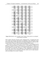
6 subsites (rotated)
Figure 4.4 Adaptive body bias test-chip [7]. (© 2002 IEEE)
Figure 4.4 shows an adaptive body bias test-chip implemented in the
150nm CMOS technology generation [7]. Each test-chip die contains 21
“subsites” distributed over a 4.5×5.3mm
2
area in two orthogonal
80 James Tschanz
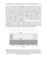
orientations. Each of these subsites (Figure 4.5) represents a circuit block
of a microprocessor design and contains a complete adaptive body bias
(ABB) generator and control circuit in addition to critical path blocks. One
critical path from this circuit block is replicated and a target clock
frequency φ is applied externally. This represents the desired frequency of
operation for the circuit block. The delay of the critical path replica is
compared to the incoming clock period through the use of a phase detector
circuit, and the output from this phase detector drives a counter and D/A
converter to generate the body bias voltage. This forms a feedback circuit
which automatically adjusts the body bias until the delay of the critical
path matches the incoming clock period. To find the optimum body bias
voltage for each die, different target frequencies can be applied to the input
clock, and after the body bias adapts to meet the target frequency, the
leakage of the die is measured. The body bias voltage which gives the
maximum performance subject to the power constraint is the optimum
voltage which is chosen for that die sample.
5-bit
counter
V
REF
V
CCA
-
+
V
BP
φ
Critical path
Circuit block
(CUT)
V
CC
V
SS
V
BP,ext
V
BN,ext
PD
Bias selector
2R2R 2R 2R 2R 2R
RRR
R
f
R
÷
Phase detector
Figure 4.5 Key circuit elements of one subsite of adaptive body bias test-chip [7].
(© 2002 IEEE)
Measurement results for adaptive body bias (ABB) as compared to no
body bias (NBB) are shown in Figure 4.6. All fabricated dies must meet a
minimum performance specification, as shown by the vertical dashed line
Chapter 4 Dynamic Adaptation Using Body Bias, Supply Voltage, and Frequency 81
0
1
2
3
4
5
6
0.925 1 1.075 1.15 1.225
Normalized frequency
Normalized leaka
g
e
0%
20%
40%
60%
80%
100%
Die count
NBB
ABB
Accepted
dies:
0%
110C
1.1V
ABB
NBB
σ/μ=0.69%
σ/μ=4.1%
0
1
2
3
4
5
6
0.925 1 1.075 1.15 1.225
Normalized frequency
Normalized leaka
g
e
0%
20%
40%
60%
80%
100%
Die count
NBB
ABB
Accepted
dies:
0%
110C
1.1V
ABB
NBB
σ/μ=0.69%
σ/μ=4.1%
Figure 4.6 Measurement results: comparison of no body bias (NBB) and adaptive
body bias (ABB) [7]. (© 2002 IEEE)
at a frequency of 1, as well as a maximum leakage specification dictated
by the platform total power requirements. This maximum leakage line is
slanted reflecting that the fast dies run at higher frequency which results in
higher dynamic power consumption – therefore their allowed leakage
power is low. Application of ABB reduces die-to-die frequency variations
(σ/μ) by an order of magnitude, and 100% of the dies become acceptable
as compared with only 50% accepted dies for NBB. In addition, 30% of
the dies are now in the highest frequency bin allowed by the power density
limit.
The above procedure is very effective for compensating the die-to-die
parameter variations; however, since only one bias voltage is used per die,
it is not possible to compensate any variations across the die. In order to
reduce the impacts of within-die variations as well, multiple bias voltages
can be employed and individually tuned. The number of body bias regions
used across the die depends on the correlation distance of the within-die
variation components as well as the area overhead and testing complexity
involved in generating multiple bias voltages on the die. Figure 4.7
demonstrates the gains possible by using multiple bias voltages – in this
example, each of the 21 subsites on the test-chip receives its own unique
body bias voltage. In this case, frequency variation is reduced by another
4× as compared to the die-to-die ABB, and 99% of the dies are now in the
highest-revenue bin.
82 James Tschanz
0
1
2
3
4
5
6
0.925 1 1.075 1.15 1.225
Normalized frequency
Normalized leaka
g
e
0%
20%
40%
60%
80%
100%
Die count
ABB
WID-ABB
Accepted
dies:
0%
110C
1.1V
WID-ABB
ABB
σ/μ=0.21%
σ/μ=0.69%
0
1
2
3
4
5
6
0.925 1 1.075 1.15 1.225
Normalized frequency
Normalized leaka
g
e
0%
20%
40%
60%
80%
100%
Die count
ABB
WID-ABB
Accepted
dies:
0%
110C
1.1V
WID-ABB
ABB
σ/μ=0.21%
σ/μ=0.69%
Figure 4.7 Measurement results: comparison of ABB and within-die ABB [7].
(© 2002 IEEE)
4.2.2 Adaptive Supply Voltage
Supply voltage can be used in the same way as body bias to counteract the
effects of process variations. While frequency binning is the simplest way
to compensate die-to-die variations and recover dies which exceed the
power requirement, adaptive V
CC
provides two significant benefits over
simple frequency binning. First, dies that violate the power constraint will
have V
CC
reduced in tandem with their natural operating frequencies,
which provides better power savings than frequency reduction alone. In
contrast to simple frequency reduction, lowering V
CC
reduces standby
leakage power as well, while switching power is reduced in a cubic
manner. Therefore, lowering V
CC
and frequency together allows dies to be
accepted in a higher frequency bin than with simple frequency binning
alone. Second, dies which are too slow can be recovered by increasing
their V
CC
to increase their natural operating frequency and move them to
the highest frequency bin allowed by the active power limit. Gate-oxide
reliability considerations limit the maximum allowed V
CC
; however, this
constraint is not usually a problem for mobile processors with V
CC
lower
than the maximum allowed by the process.
Evaluation of the impact of adaptive supply voltage has been performed
on the same 150nm CMOS test-chip as was described above in the body
bias section [8]. For these measurements, it is assumed that the processor
is a low-power product which is running at a V
CC
below the V
MAX
limit.
Therefore, slow dies can be sped up by increasing the V
CC
, while leaky
Chapter 4 Dynamic Adaptation Using Body Bias, Supply Voltage, and Frequency 83
dies can be recovered by reducing the V
CC
. As shown in Figure 4.8,
applying adaptive V
CC
improves the mean die frequency as well as the
number of parts in the highest frequency bin. However, effectiveness of
adaptive V
CC
depends critically on the voltage resolution provided by the
voltage regulator module. Using 50mV resolution instead of 20mV renders
the technique ineffective.
0%
20%
40%
60%
80%
0.85 0.90 0.95 1.00 1.05
Frequency bin (normalized)
Accepted die count
Fixed Vcc: 1.05V
Adaptive Vcc (50mV
resolution)
Adaptive Vcc (20mV
resolution
)
0%
10%
20%
30%
40%
50%
-9% -7% -4% -2% 0% 2% 4%
Vcc (normalized)
Accepted die count
p
Nominal Vcc: 1.05V
Adaptive Vcc
Ada
p
tive Vcc+Vbs
Figure 4.8 (a) Comparison of fixed V
CC
and adaptive V
CC
, (b) Comparison of
adaptive V
CC
and adaptive V
CC
+V
BS
[8]. (© 2003 IEEE)
Using adaptive V
CC
in conjunction with adaptive body bias (adaptive
V
BS
) is more effective than using either of them individually (Figure 4.8b).
In this combined scheme (adaptive V
CC
+V
BS
), a single V
CC
and
NMOS/PMOS V
BS
combination is used per die to move it to the highest
frequency bin subject to the active power limit. Adaptive V
BS
uses FBB to
speed up dies that are too slow, and RBB to reduce frequency and leakage
power of dies that are too fast and leaky. Adaptive V
CC
+V
BS
, on the other
hand, recovers these dies above the active power limit by (1) first lowering
V
CC
and natural operating frequency together to bring the sum total of their
switching and leakage powers well below the active power limit and (2)
then applying FBB to speed them up and move them to the highest
frequency bin allowed by the active power limit. As a result, more dies use
lower V
CC
values than adaptive V
CC
. In addition, more dies use FBB,
instead of RBB, compared to adaptive V
BS
(Figure 4.9). Since the
effectiveness of RBB for leakage power reduction diminishes with
technology scaling [4], adaptive V
CC
+V
BS
will be more effective in future
technology generations than adaptive V
BS
alone. Bias voltages for NMOS
and PMOS transistors are typically generated using on-die circuitry and
routed to transistor wells using a separate bias grid, incurring an area
overhead of 2–4%.
84 James Tschanz
2% 25%
Die count:
-0.4
-0.3
-0.2
-0.1
0
0.1
0.2
0.3
0.4
PMOS body bias (V
)
P FBB
N
RBB
P FBB
N FBB
P RBB
N
RBB
P RBB
N FBB
(a) Adaptive Vbs
2% 25%
Die count:
-0.4
-0.3
-0.2
-0.1
0
0.1
0.2
0.3
0.4
PMOS body bias (V
)
P FBB
N
RBB
P FBB
N FBB
P RBB
N
RBB
P RBB
N FBB
(a) Adaptive Vbs
-0.4
-0.3
-0.2
-0.1
0
0.1
0.2
0.3
0.4
-0.4 -0.3 -0.2 -0.1 0 0.1 0.2 0.3 0.4
NMOS body bias (V)
PMOS body bias (V
)
P FBB
N
RBB
P FBB
N FBB
P RBB
N
RBB
P RBB
N FBB
(b) Adaptive Vcc+Vbs
-0.4
-0.3
-0.2
-0.1
0
0.1
0.2
0.3
0.4
-0.4 -0.3 -0.2 -0.1 0 0.1 0.2 0.3 0.4
NMOS body bias (V)
PMOS body bias (V
)
P FBB
N
RBB
P FBB
N FBB
P RBB
N
RBB
P RBB
N FBB
(b) Adaptive Vcc+Vbs
-0.4 -0.3 -0.2 -0.1 0 0.1 0.2 0.3 0.4
NMOS body bias (V)
-0.4 -0.3 -0.2 -0.1 0 0.1 0.2 0.3 0.4
NMOS body bias (V)
Figure 4.9 Optimal body bias voltages chosen for (a) adaptive V
BS
, (b) adaptive
V
CC
+V
BS
[8]. (© 2003 IEEE)
4.3 Dynamic Variation Compensation
4.3.1 Dynamic Body Bias
Body bias can also be used in a dynamic sense as part of a power
management scheme or to compensate dynamic variations. Due to
advanced power control features, microprocessors can experience a very
wide range of activity factors during normal operation – ranging from very
high activity for tasks which are heavily computationally intensive to very
low activity when the processor is in standby mode. Therefore it is
impossible to find the device threshold voltage, supply voltage, and
frequency which is energy optimal across all usage conditions. Body bias
provides a way to adjust the threshold voltage dynamically to improve
performance during active mode while saving power in standby mode.
When the processor is actively running computations, the activity factor
is high, and typically dynamic power dominates over the leakage power. In
this case, forward body bias can be applied to lower the threshold voltage
and improve performance. Alternately, the device threshold voltage can be
increased in the process so that when FBB is applied, it is lowered to the
original target value. Applying FBB in this manner also has the advantage
of improving the short-channel effects of the devices compared to
lowering the V
T
through process only. When the processor goes into an
idle or standby mode, the power is dominated by transistor leakage. Zero
or reverse body bias can then be applied to raise the threshold voltage and
Chapter 4 Dynamic Adaptation Using Body Bias, Supply Voltage, and Frequency 85
reduce the leakage. In this manner, the processor operates much more
efficiently in both active and standby modes.
Scan
FIFO
Scan
out
Sleep
ALU
Body bias
Control
Figure 4.10 Dynamic ALU test-chip with on-chip PMOS body bias [9].
(© 2003 IEEE)
An implementation of dynamic body bias for power control is shown in
Figure 4.10. This test-chip in 130nm CMOS technology [9] includes a 32-
bit dynamic ALU with on-chip dynamic body bias for the PMOS
transistors. The body bias circuitry consists of two main blocks: a central
bias generator (CBG) and many distributed local bias generators (LBGs)
(Figure 4.11). The function of the CBG is to generate a process, voltage,
and temperature-invariant reference voltage which is then routed to the
local bias generators. The CBG uses a scaled bandgap circuit to generate a
reference voltage which is 450mV below the bandgap supply V
CCA
– this
represents the amount of forward bias to apply in active mode. This
reference voltage is then routed to all of the distributed local bias
generators, shielded on both sides by V
CCA
. The function of the LBG is to
translate this voltage, referenced to V
CCA
, to a body voltage which is
referenced to the local block V
CC
. This ensures that any variations in the
local V
CC
will be tracked by the body voltage, maintaining a constant
450mV of FBB. Translation of the reference is accomplished through the
use of a current mirror followed by a voltage buffer to drive the final n-
well load. Low-frequency tracking of supply variations is handled by the
current mirror while a capacitor provides the high-frequency tracking. In
idle mode, the current mirror is disabled and a zero-bias switch transistor
connects the body to V
CC
, applying zero body bias for leakage reduction. A
total of 40 distributed LBGs are used to bias the ALU, and the total area
overhead for this body bias technique is 6–8%, including the bias
generators as well as the additional routing required to separate the body
terminals from the supply.
86 James Tschanz
Vcca
Vcca - 450mV
(shielded)
Scaled
bandgap
Local Vcc - 450mV
Current
mirror
Local Bias Generators
Central Bias
Generator
Zero-bias
switch
Vcca
Vcca
Control
Vref
Figure 4.11 Bias generator circuits for dynamic ALU test-chip [9].
(© 2003 IEEE)
The adder operational frequency ranges from 3GHz (1.05V) to 4.2GHz
(1.4V) when zero body bias (ZBB) is applied to the PMOS transistors in
the core (Figure 4.12a). If the dynamic body bias circuitry is enabled to
apply 450mV FBB to the core, the frequency improves by 3–7%. To
achieve a target frequency of 4.05GHz, the supply voltage must be set to
1.35V when no body bias is used but can be lowered to 1.28V with FBB.
This supply voltage reduction results in lower switching power for the
FBB design at the same clock frequency. When the adder is put into
standby mode, ZBB is used for the core, and this results in a leakage
reduction of 2×. Total power savings for the ALU at a typical activity
profile are shown in Figure 4.12b – for this example, the dynamic bias
achieves 8% total power reduction. Therefore dynamic body biasing
allows the frequency improvement due to FBB coupled with the reduced
leakage power of ZBB.
0
2
4
6
8
10
12
Clock gating only Clock gating +
body bias
Tota power (mW)
1.28V 1.28V
Switching
Leakage
Overhead
8%
savings
↓
45%
LBG
only
0
2
4
6
8
10
12
Clock gating only Clock gating +
body bias
Tota power (mW)
1.28V 1.28V
Switching
Leakage
Overhead
8%
savings
↓
45%
LBG
only
2.5
3
3.5
4
4.5
1 1.1 1.2 1.3 1.4 1.5
Vcc (V)
Frequency (GHz)
ZBB
450mV FBB to core
4.05GHz
75 ° C, No sleep transistor
1.28V
1.35V
5% lower V
CC
for
same frequency
5% frequency
increase
2.5
3
3.5
4
4.5
1 1.1 1.2 1.3 1.4 1.5
Vcc (V)
Frequency (GHz)
ZBB
450mV FBB to core
4.05GHz
75 ° C, No sleep transistor
1.28V
1.35V
5% lower V
CC
for
same frequency
5% frequency
increase
Figure 4.12 (a) Maximum frequency vs. supply voltage for ALU with and
without body bias. (b) Typical power savings due to dynamic body bias [9].
(© 2003 IEEE)
Chapter 4 Dynamic Adaptation Using Body Bias, Supply Voltage, and Frequency 87
4.3.2 Dynamic Supply Voltage, Body Bias, and Frequency
While static techniques such as clock tuning, adaptive body bias, and
adaptive supply voltage can effectively compensate process variations,
other variations such as temperature, voltage droops, noise, and transistor
aging are dynamic and change throughout the lifetime of the processor.
These cannot be compensated using a static technique and are typically
guardbanded using either reduced frequency or higher supply voltage. This
guardbanding is expensive in terms of performance and power and is
becoming prohibitive as design margins shrink. To achieve an energy-
efficient microprocessor which operates correctly in the presence of these
variations, a method of sensing the environment and responding by
changing voltage, body bias, or frequency is necessary. In this section, we
describe one implementation of a dynamic adaptive processor design.
4.3.2.1 Design Details
The test-chip in 90nm CMOS technology (Figure 4.13) contains a TCP
offload accelerator core, a data input buffer, V
CC
droop sensors, thermal
sensors, a dynamic adaptive biasing (DAB) control unit, distributed noise
injectors, body bias generators, and a three-PLL dynamic clocking unit
[10]. The DAB controller receives inputs from the thermal sensors and
droop detectors. Average supply current is sensed by the off-chip voltage
regulator module (VRM), and digitally communicated to the DAB
controller on chip. The programmable noise injectors are used to generate
various supply noises and load currents, in addition to that generated by
Figure 4.13 Block diagram of the dynamic adaptive TCP/IP processor [10].
(© 2007 IEEE)
TCP/IP
processor
PLL0
PLL1
DAB
Control
Thermal
sensor
Div
PMOS
CBG
NMOS
CBG
core clk
gate
Droop
sensor
Time
Time
PLL2
NMOS body bias
PMOS body bias
I/O clk
Noise
injector
F
0
F
1
F
2
ctrl
VRM
(off-die)