Adaptive Techniques for Dynamic Processor Optimization_Theory and Practice Episode 1 Part 7 ppsx
Bạn đang xem bản rút gọn của tài liệu. Xem và tải ngay bản đầy đủ của tài liệu tại đây (786.84 KB, 20 trang )
Chapter 5 Adaptive Supply Voltage Delivery for U-DVS Systems 109
5.3.2 DC–DC Converter Topologies for U-DVS
5.3.2.1 Linear Regulators
Low-dropout (LDO) linear regulators [22] are widely used to supply ana-
log and digital circuits and feature in several standalone or embedded
power management ICs. The main advantage of LDO’s is that they can be
completely on-chip, occupy very little area, and offer good transient and
ripple characteristics, together with being a low-cost solution. Using
LDO’s for U-DVS, however, is detrimental because of the linear loss of
efficiency in an LDO. A linear regulator essentially controls the resistance
of a transistor in order to regulate the output voltage. As a result, the cur-
rent delivered to the load flows directly from the battery and hence the
maximum efficiency achievable is limited to the ratio of the output voltage
to the input voltage. Thus, the farther away the load voltage is from the
battery voltage, the lower the efficiency of the LDO. This hampers the po-
tential savings in power consumption that can be achieved by lowering the
voltage through DVS.
5.3.2.2 Inductor-Based DC–DC Converter
The most efficient DC–DC voltage converters are inductor-based switch-
ing regulators, which normally generate a reduced DC voltage level by fil-
tering a pulse-width modulated (PWM) signal through a simple LC filter.
A buck-type regulator can generate different DC voltage levels by varying
the duty-cycle of the PWM signal. Given ideal devices and passives, an
inductor-based DC–DC converter can theoretically achieve 100% effi-
ciency independent of the load voltage being delivered. Moreover, in the
context of DVS systems, scaling the output voltage can be done with com-
pletely digital control circuitry [21] which consumes very little overhead
power. An implementation of an inductor-based switching regulator for
minimum energy operation is described in Section 5.3.3.1C. While buck
converters [23] can operate at very high efficiencies (>90%), they gener-
ally require off-chip filter components. This might limit their usefulness
for integrated power converter applications. Integrating the filter inductor
on-chip requires very high switching frequencies (>100MHz) in order to
minimize area consumed. This increases the switching losses in the con-
verter and together with the increase in conduction losses due to the low
inductor Q-factors achievable on-chip severely affects the efficiency that
can be obtained out of the converter.
110 Yogesh K. Ramadass, Joyce Kwong, Naveen Verma, Anantha Chandrakasan
5.3.2.3 Switched Capacitor-Based DC–DC Converter
U-DVS systems often require multiple on-chip voltage domains with each
domain having specific power requirements. A switched capacitor (SC)
DC–DC converter is a good choice for such battery-operated systems be-
cause it can minimize the number of off-chip components and does not re-
quire any inductors. Previous implementations of SC converters (charge
pumps) have commonly used off-chip charge-transfer capacitors [24] to
output high load power levels. A SC DC–DC converter which integrates
the charge-transfer capacitors was described in [25].
C
load
I
O
V
O
= V
NL
−ΔV
C
C
V
BAT
Φ
1
Φ
2
Φ
2
Φ
1
Φ
2
C
load
I
O
V
O
= V
NL
−ΔV
C
C
V
BAT
Φ
1
Φ
2
Φ
2
Φ
1
Φ
2
Figure 5.13 A switched capacitor voltage divide-by-2 circuit.
Consider the divide-by-2 circuit shown in Figure 5.13. The charge-
transfer (flying) capacitors are equal in value and help in transferring
charge from the battery to the load. During phase Φ
1
of the system clock,
the charge-transfer capacitors get charged from the battery (V
BAT
). In the
Φ
2
phase of the clock, they dump the charge gained onto the load. At no
load, this circuit tries to maintain the output voltage V
O
at V
BAT
/2, where
V
BAT
is the battery voltage. The actual value of V
O
that the circuit settles
down to is dependent on the load current I
O
, the switching frequency, and
C. Let the circuit deliver a load voltage V
O
= V
NL
– ΔV, where V
NL
is the
no-load voltage for this topology. The SC converter limits the maximum
efficiency that can be achieved in this case to
η
lin
= (1 – ΔV/V
NL
). Thus,
the farther away V
O
is from V
NL
(i.e., higher ΔV), the smaller the maxi-
mum efficiency that can be achieved by this topology. This is a fundamen-
tal problem with charge transfer using only capacitors and switches. The
linear efficiency loss is similar to linear regulators. However, with SC
converters, it is possible to switch in different gain-settings whose no-load
Chapter 5 Adaptive Supply Voltage Delivery for U-DVS Systems 111
output voltage is closer to the load voltage desired. Apart from the linear
conduction loss, losses due to bottom-plate parasitics of on-chip capacitors
and switching losses limit the efficiency of the SC DC–DC converter [26].
The efficiency achievable in a switched capacitor system is in general
smaller than that can be achieved in an inductor-based switching regulator
with off-chip passives. Furthermore, multiple gain-settings and associated
control circuitry are required in a SC DC–DC converter to maintain effi-
ciency over a wide voltage range. However, for on-chip DC–DC convert-
ers, a SC solution might be a better choice, when the trade-offs relating to
area and efficiency are considered. Furthermore, the area occupied by the
switched capacitor DC–DC converter is scalable with the load power de-
mand, and hence the switched capacitor DC–DC converter is a good solu-
tion for low-power on-chip applications.
SWITCH
MATRIX
I
O
V
O
V1p8
V
BAT
(1.2V)
Φ
1
Φ
2
Φ
1by3
Φ
2by3
enW2
enW4
Non-Overlapping
Clock Generator
V
ref
clk
COMP
C
load
AUTOMATIC
FREQUENCY
SCALER
V
O
Φ
2
clk4X
DAC
clk
÷
V
ref
Φ
1
Φ
2
Φ
1by3
Φ
2by3
7
SWITCH
MATRIX
I
O
V
O
V1p8
V
BAT
(1.2V)
Φ
1
Φ
2
Φ
1by3
Φ
2by3
enW2
enW4
Non-Overlapping
Clock Generator
V
ref
clk
COMP
C
load
AUTOMATIC
FREQUENCY
SCALER
V
O
Φ
2
clk4X
DAC
clk
÷
V
ref
Φ
1
Φ
2
Φ
1by3
Φ
2by3
7
Figure 5.14 Architecture of a switched capacitor DC–DC converter with on-chip
charge-transfer capacitors. (© [2007] IEEE)
A SC DC–DC converter that employs five different gain-settings with
ratios 1:1, 3:4, 2:3, 1:2, and 1:3, is described in [26]. The switchable gain-
settings help the converter to maintain a good efficiency as the load volt-
age delivered varies from 300mV to 1.1V. Figure 5.14 shows the architec-
ture of the SC DC–DC converter. At the core of the system is the switch
matrix which contains the charge-transfer capacitors and the charge-
transfer switches. A suitable gain-setting is chosen depending on the refer-
ence voltage V
ref
, which is set digitally. A pulse frequency modulation
(PFM) mode control is used to regulate the output voltage to the desired
value. Bottom-plate parasitics of the on-chip capacitors significantly affect
the efficiency of the converter. A divide-by-3 switching scheme [26] was
employed to mitigate the effect due to bottom-plate parasitics and improve
efficiency. The switching losses are scaled with change in load power by
112 Yogesh K. Ramadass, Joyce Kwong, Naveen Verma, Anantha Chandrakasan
the help of the automatic frequency scaler block. This block changes the
switching frequency as the load power delivered changes, thereby reducing
the switching losses at low load.
The efficiency of the SC converter with change in load voltage while
delivering 100μW to the load from a 1.2V supply is shown in Figure 5.15.
The converter was able to achieve >70% efficiency over a wide range of
load voltages. An increase in efficiency of close to 5% can be achieved by
using divide-by-3 switching.
0.3 0.4 0.5 0.6 0.7 0.8 0.9 1 1.1
50
55
60
65
70
75
80
85
90
95
Load Voltage (V)
Efficiency (%)
Measured - divby3 switching
Measured - normal switching
Theoretical
0.3 0.4 0.5 0.6 0.7 0.8 0.9 1 1.1
50
55
60
65
70
75
80
85
90
95
Load Voltage (V)
Efficiency (%)
Measured - divby3 switching
Measured - normal switching
Theoretical
Figure 5.15 Efficiency of the switched capacitor DC–DC converter with change
in load voltage. (© [2007] IEEE)
5.3.3 DC–DC Converter Design and Reference Voltage
Selection for Highly Energy-Constrained Applications
While dynamic voltage scaling is a popular method to minimize power
consumption in digital circuits given a performance constraint, the same
circuits are not always constrained to their performance-intensive mode
during regular operation. There are long spans of time when the perform-
ance requirement is highly relaxed. There are also certain emerging en-
ergy-constrained applications where minimizing the energy required to
complete operations is the main concern. For both these scenarios, operat-
ing at the minimum energy operating voltage of digital circuits has been
proposed as a solution to minimize energy. The minimum energy point
Chapter 5 Adaptive Supply Voltage Delivery for U-DVS Systems 113
(MEP) is defined as the operating voltage at which the total energy con-
sumed per desired operation of a digital circuit is minimized. Switching
energy of digital circuits reduces quadratically as V
DD
is decreased below
V
T
(i.e., sub-threshold operation), while the leakage energy increases ex-
ponentially. These opposing trends result in the minimum energy point.
The MEP is not a fixed voltage for a given circuit and can vary widely de-
pending on its workload and environmental conditions (e.g., temperature).
Any relative increase in the active energy component of the circuit due to
an increase in the workload or activity of the circuit decreases the mini-
mum energy operating voltage. On the other hand, a relative increase of
the leakage energy component due to an increase in temperature or the du-
ration of leakage over an operation pushes the minimum energy operating
voltage to go up. This makes the circuit go faster, thereby not allowing the
circuit to leak for a longer time. By tracking the MEP as it varies, energy
savings of 50–100% has been demonstrated [27] and even greater savings
can be achieved in circuits dominated by leakage. This motivates the de-
sign of a minimum energy tracking loop that can dynamically adjust the
operating voltage of arbitrary digital circuits to their MEP.
5.3.3.1 Minimum Energy Tracking Loop
Figure 5.16 shows the architecture of the minimum energy tracking loop.
The objective of this loop is to track the minimum energy operating
voltage of the load circuit. The load circuit (FIR filter) is powered from an
off-chip voltage source through a DC–DC converter and is clocked by a
CLK
var
V
DD
V
ref
Energy
Sensor
Circuitry
Load
(FIR Filter)
DC-DC
Converter
and Control
Energy
Minimization
Algorithm
Critical Path
Replica Ring
Oscillator
COMP
Energy /
operation
DAC
C
load
AV
ref
V
DD
V
BAT
7
13
CLK
var
V
DD
V
ref
Energy
Sensor
Circuitry
Load
(FIR Filter)
DC-DC
Converter
and Control
Energy
Minimization
Algorithm
Critical Path
Replica Ring
Oscillator
COMP
Energy /
operation
DAC
C
load
AV
ref
V
DD
V
BAT
7
13
Figure 5.16 Architecture of the minimum energy tracking loop. (© [2007] IEEE)
114 Yogesh K. Ramadass, Joyce Kwong, Naveen Verma, Anantha Chandrakasan
critical path replica ring oscillator which automatically scales the clock
frequency of the FIR filter with change in load voltage. The energy sensor
circuitry calculates on-chip, the energy consumed per operation of the load
circuit at a particular operating voltage. It then passes the estimate of the
energy/operation (E
op
) to the energy minimizing algorithm, which uses the
E
op
to suitably adjust the reference voltage to the DC–DC converter. The
DC–DC converter then tries to get V
DD
close to the new reference voltage,
and the cycle repeats till the minimum energy point is achieved. The only
off-chip components of this entire loop are the filter passives of the induc-
tor-based switching DC–DC converter.
A. Energy Sensing Technique
The key element in the minimum energy tracking loop is the energy sensor
circuit which computes the E
op
of the load circuit at a given reference volt-
age. Methods to measure E
op
, by sensing the current flow through the DC–
DC converter’s inductor [28], dissipate a significant amount of overhead
power. The approach is more complicated at sub-threshold voltages be-
cause the current levels are very low. Furthermore, an estimate of the en-
ergy consumed per operation is what is required and not just the current
which only gives an idea of the load power. The methodology used here, to
estimate E
op
, does not require any high-gain amplifiers or analog circuit
blocks.
The DC–DC converter while operating in steady state keeps the output
voltage close to the reference voltage. Just before the energy sense cycle
begins, the DC–DC converter is disabled. The energy sense cycle consists
of N operations of the digital circuit where the value N can be 32 or 64.
Assuming that the voltage across the storage capacitor of the DC–DC con-
verter, C
load
, falls from the reference voltage V
1
to V
2
in the course of N op-
erations of the digital circuit, E
op
at the voltage V
1
is equal to
( )
N2
V
2
2
2
−
=
1load
op
V C
E
(5.1)
To measure E
op
accurately, V
2
should be close in value (within 20mV) to
V
1
. Measuring E
op
by digitizing V
1
and V
2
using conventional ADCs would
require at least 11 bits of precision in the ADC. This could prove costly in
terms of power consumed. An energy-efficient approach to obtain E
op
is to
observe that, by design, V
1
is very close to V
2
. Thus, the following simpli-
fication can be applied within an acceptable error:
Chapter 5 Adaptive Supply Voltage Delivery for U-DVS Systems 115
()() ()
NN2
211load2121load
op
VVVC VV VV C
E
−
≈
−+
=
(5.2)
()
211op
VVVE −∝
(5.3)
From Equation (5.3), it can be seen that the energy consumed per opera-
tion is directly proportional to the product of V
1
and V
1
– V
2
. Since, the
digital representation of V
1
, which is the reference voltage to the DC–DC
converter, is already known, only the digital value for the voltage differ-
ence (V
1
– V
2
)
is required to estimate E
op
. This voltage difference is ob-
tained digitally using a fixed frequency clock, a constant current sink, a
comparator, and a counter [27]. These blocks help in quantizing voltage
into time steps, as in an integrating ADC [29]. The number of fixed fre-
quency clock cycles obtained from the counter is directly proportional to
V
1
– V
2
. This quantity is then digitally multiplied with V
1
which is the ref-
erence voltage V
ref
to the DC–DC converter. The product of these two
quantities gives an estimate of the energy consumed per operation by the
digital circuit at voltage V
1
. The estimate obtained is a normalized repre-
sentation of the absolute value of the energy consumed per operation. This
estimate is passed on to the energy minimization algorithm block.
B. Energy Minimization Algorithm
Once the estimate of the energy per operation is obtained, the minimum
energy tracking algorithm uses this to suitably adjust the reference voltage
to the DC–DC converter. The minimum energy tracking algorithm is a
slope-tracking algorithm which makes use of the single minimum, concave
nature of the E
op
versus V
DD
curve (see Figure 5.1b). The algorithm starts
by setting the reference voltage V
ref
to some initial value. The energy per
operation at this voltage is computed and stored in a minimum energy reg-
ister (E
op,min
). The tracking loop then automatically increments V
ref
by one
voltage step. Once V
DD
settles at this newly incremented voltage, E
op
is
computed again and is compared with the value stored in the minimum en-
ergy register. At this point, if the newly computed E
op
is found to be
smaller, the loop then just keeps incrementing V
ref
at fixed voltage steps,
while at the same time updating E
op,min
till the minimum is achieved. The
other possibility is that the newly computed energy per operation is higher
than that stored in the minimum energy register. In this case, the loop
changes direction and begins to decrement V
ref
. The loop keeps decrement-
ing V
ref
till the E
op
calculated is higher than E
op, min
at which time the loop
116 Yogesh K. Ramadass, Joyce Kwong, Naveen Verma, Anantha Chandrakasan
increments V
ref
by one voltage step to get to the MEP and shuts down.
Figure 5.17 shows the minimum energy tracking loop in operation for a
7-tap FIR filter load circuit.
The voltage step used by the tracking algorithm is usually set to 50mV.
A large voltage step leads to coarse tracking of the MEP, with the possibil-
ity of missing the MEP. On the other hand, keeping the voltage step too
small might lead to the loop settling at the non-minimum voltage due to er-
rors involved in computing E
op
[30]. The E
op
versus V
DD
curve is shallow
near the MEP, and hence a 50mV step leads to a very close approximation
of the actual minimum energy consumed per operation. The MEP tracking
loop can be enabled by a system controller as needed depending on the ap-
plication, or periodically by a timer to track temperature variations.
V
DD
Loop Start
Loop Stop
V
DD
starts at 420mV V
DD
settles at 370mV
370mV
320mV
V
DD
Loop Start
Loop Stop
V
DD
starts at 420mV V
DD
settles at 370mV
370mV
320mV
Figure 5.17 Measured waveform showing the minimum energy tracking loop in
operation. (© [2007] IEEE)
Chapter 5 Adaptive Supply Voltage Delivery for U-DVS Systems 117
C. Embedded DC–DC Converter for Minimum Energy Operation
This section talks about the design of the DC–DC converter that enables
minimum energy operation. Since the minimum energy operating voltage
usually falls in the sub-threshold regime of operation, the DC–DC con-
verter is designed to deliver load voltages from 250mV to around 700mV.
The power consumed by digital circuits at these sub-threshold voltages is
exponentially smaller and hence the DC–DC converter needs to deliver ef-
ficiently load power levels of the order of micro-watts. This demands ex-
tremely simple control circuitry design with minimal overhead power to
get good efficiency. The DC–DC converter shown in Figure 5.18 is a syn-
chronous rectifier buck converter with off-chip filter components and op-
erates in the discontinuous conduction mode (DCM). It employs a pulse
frequency modulation (PFM) [31] mode of control in order to get good ef-
ficiency at the ultra-low load power levels that the converter needs to de-
liver. The PFM mode control also helps in seamlessly disabling the con-
verter when energy sensing takes place, thereby making it feasible to use
the energy-sensing technique described in Section 5.3.3.1A.
The reference voltage to the converter is set digitally by the minimum
energy tracking loop and is converted to an analog value by an on-chip
DAC before it is fed to the comparator. The comparator compares V
DD
with this reference voltage and when V
DD
is found to be smaller generates
a pulse of fixed width to turn the PMOS power transistor ON and ramp up
the inductor current. A variable pulse-width generator to achieve zero-
current switching is used for the NMOS power transistor. The comparator
is clocked by a divided and level-converted version of the system clock
which feeds the load FIR filter.
CLK
var
V
BAT
(1.2V)
AV
ref
COMP
Off-chip
L
C
load
כ
כ
כ
כ
EN
Fixed
Pulse Width
Generator
Variable
Pulse Width
Generator
V
ref
V
DD
Divider and Level
Converter
(from DAC)
CLK
var
V
BAT
(1.2V)
AV
ref
COMP
Off-chip
L
C
load
כ
כ
כ
כ
EN
Fixed
Pulse Width
Generator
Variable
Pulse Width
Generator
V
ref
V
DD
Divider and Level
Converter
(from DAC)
Figure 5.18 DC–DC Converter architecture. (© [2007] IEEE)
118 Yogesh K. Ramadass, Joyce Kwong, Naveen Verma, Anantha Chandrakasan
V
ref
0
1
2
3
Decoder
τ
1
τ
2
τ
3
τ
4
τ
P
V
BAT
NMOS
PULSE
PMOS
PULSE
i
L
(t)
τ
1
τ
2
τ
4
τ
3
Variable Pulse-Width Generator
V
ref
0
1
2
3
Decoder
τ
1
τ
2
τ
3
τ
4
τ
P
V
BAT
NMOS
PULSE
PMOS
PULSE
i
L
(t)
τ
1
τ
2
τ
4
τ
3
τ
P
V
BAT
NMOS
PULSE
PMOS
PULSE
i
L
(t)
τ
1
τ
2
τ
4
τ
3
Variable Pulse-Width Generator
Figure 5.19 Approximate zero-current switching block. (© [2007] IEEE)
The ultra-low load power levels demand extremely simple control cir-
cuitry to achieve good efficiency. This precludes the usage of high-gain
amplifiers to detect zero-crossing and thereby do zero-current switching
[31]. In order to keep the control circuitry simple and consume little over-
head power, an all-digital open-loop control as shown in Figure 5.19 is
used to achieve zero-current switching. The variable pulse-width generator
block which accomplishes this functions as follows: When the comparator
senses that V
DD
has fallen below the reference voltage, a PMOS ON pulse
of fixed pulse width τ
P
is generated. This ramps up the inductor current
from zero. Once the PMOS is turned OFF, the NMOS power transistor is
turned ON after a fixed delay. This ramps down the inductor current. Ide-
ally, in the discontinuous conduction mode (DCM) used in this implemen-
tation, the NMOS has to be turned OFF just when the inductor current
reaches zero. The amount of time it takes for the inductor current to reach
zero is dependent on the reference voltage set, and in steady state, the ratio
of the NMOS to PMOS ON-times is given by the following equation:
DD
DDBAT
P
N
V
VV −
=
τ
τ
(5.4)
where τ
N
and τ
P
are the NMOS and PMOS ON-times and V
BAT
is the bat-
tery voltage. Thus, by fixing τ
P
, the values of τ
N
for specific load voltages
can be predetermined. The variable pulse-width generator block then
suitably multiplexes these predetermined delays depending on the refer-
ence voltage set to achieve approximate zero-current switching. Increasing
the number of these delay elements and the complexity of the multiplexer
block gives a better approximation to zero-current switching. Since only
the ratios of the NMOS and PMOS ON-time pulse widths need to match,
this scheme is independent of absolute delay values and any tolerance in
the inductor value. Furthermore, it consumes very little overhead power.
Chapter 5 Adaptive Supply Voltage Delivery for U-DVS Systems 119
1 10 100
60
65
70
75
80
85
90
Load Power (
μ
W)
Efficiency (%)
Figure 5.20 Efficiency of the inductor-based switching regulator embedded within
the minimum energy tracking loop. (© [2007] IEEE)
With the help of the above-mentioned efficiency improvement tech-
niques, the DC–DC converter was able to achieve an efficiency >80% at
an extremely low load power level of 1μW as shown in Figure 5.20. While
the switching and conduction losses bring down efficiency at load power
levels of 100μW and above, the leakage losses kick in at lower load levels
bringing the efficiency further down. The simplicity of the control blocks
helps to maintain good efficiency at these ultra-low load power levels.
The proposed minimum energy tracking loop is non-intrusive, thereby
allowing the load circuit to operate without being shut down. At the same
time, it computes the energy per operation of the actual circuit and not of
any replica. This eliminates the problems of designing a replica circuit that
can track the energy behavior of a load circuit over varying operating con-
ditions. The tracking methodology is independent of the size and type of
digital circuit being driven and the topology of the DC–DC converter.
5.4 Conclusion
Dynamic voltage scaling is a popular method to minimize power consump-
tion in digital circuits given a performance constraint. By introducing the
capability of sub-threshold operation, DVS systems can be made to operate
120 Yogesh K. Ramadass, Joyce Kwong, Naveen Verma, Anantha Chandrakasan
at their minimum energy operating voltage in periods of very little activity,
leading to further savings in total energy consumed. These U-DVS systems
provide energy savings by either reducing the supply voltage to just meet
performance or operating at the minimum energy operating voltage in pe-
riods of very little activity.
The challenges involved in designing logic and memory circuits suitable
for sub-threshold operation and the methodology to overcome these chal-
lenges have been described in this chapter. Furthermore, a control circuit
to track the optimum energy point of digital circuits was presented. The
DC–DC converter used within the control loop was designed to provide
sub-threshold output voltages at very high efficiencies. The overall design
methodology and the control circuit help in saving energy consumed in
highly energy-critical applications leading to enhanced battery lifetimes
and the ability to operate out of scavenged energy.
References
[1] V. Gutnik and A. Chandrakasan, “Embedded power supply for low-power
DSP,” IEEE Trans. VLSI Syst., vol. 5, no. 4, pp. 425–435, Dec. 1997.
[2] A. Sinha and A. Chandrakasan, “Dynamic power management in wireless
sensor networks,” IEEE Design and Test of Computers, vol. 18, no. 2, pp.
62–74, March 2001.
[3] B. Zhai et al., “A 2.6pJ/Inst subthreshold sensor processor for optimal en-
ergy efficiency,” in Symp. VLSI Circuits Tech. Dig., pp. 192–193, June 2006.
[4] O. Soykan, “Power sources for implantable medical devices,” Medical
Device Manufacturing and Technology, 2002.
[5] S. Roundy, P. K. Wright, and J. Rabaey, “A study of low level vibrations as
a power source for wireless sensor nodes,” Computer Communications, vol.
26, no. 11, pp. 1131–1144, July 2003.
[6] A. Wang and A. Chandrakasan, “A 180-mV Sub-threshold FFT processor
using a minimum energy design methodology,” IEEE J. Solid-State Circuits,
vol. 40, no. 1, pp. 310–319, Jan. 2005.
[7] A. Wang, B. H. Calhoun, and A. P. Chandrakasan, “Sub-Threshold Design
for Ultra Low-Power Systems,” New York, Springer, pp. 75-–102, 2006.
[8] M. J. M. Pelgrom, A. C. J. Duinmaijer, and A. P. G. Welbers, “Matching
properties of MOS transistors,” IEEE J. Solid-State Circuits, vol. 24, no. 5,
pp. 1433–1439, Oct. 1989.
[9] J. Kwong, A. P. Chandrakasan, “Variation-driven device sizing for minimum
energy sub-threshold circuits,” IEEE Intl. Symp. on Low Power Electronics
and Design, 2006. pp. 8–13.
[10] A. Srivastava, D. Sylvester, D. Blaauw, “Statistical analysis and optimization
for VLSI: timing and power,” New York, Springer, pp. 79–132, 2005.
Chapter 5 Adaptive Supply Voltage Delivery for U-DVS Systems 121
[11] B. Zhai, S. Hanson, D. Blaauw, and D. Sylvester, “Analysis and mitigation
of variability in subthreshold design,” IEEE Intl. Symp. on Low Power Elec-
tronics and Design, pp. 20–25, 2005.
[12] J. Pille et al., “Implementation of the CELL broadband engine in a 65nm SOI
technology featuring dual-supply SRAM arrays supporting 6GHz at 1.3V,”
IEEE ISSCC Dig. Tech. Papers, pp. 322–323, Feb. 2007.
[13] N. Verma and A. Chandrakasan, “A 65nm 8T sub-V
t
SRAM employing
sense-amplifier redundancy,” IEEE ISSCC Dig. Tech. Papers, pp. 328–329,
Feb. 2007.
[14] E. Seevinck, F. List and J. Lohstroh, “Static noise margin analysis of MOS
SRAM cells,” IEEE J. Solid-State Circuits, vol. SC-22, no. 5, pp. 748–754,
Oct. 1987.
[15] M. Agostinelli, et al., “Erratic fluctuations of SRAM cache Vmin at the
90nm process technology node,” IEDM Dig. Tech. Papers, pp. 671–674,
Dec. 2005.
[16] R. Rodriguez, et al. “The impact of gate-oxide breakdown on SRAM stabil-
ity,” IEEE Electron Device Letters, vol. 23, no. 9, pp. 559–561, Sept. 2002.
[17] L. Chang, et al., “A 5.3GHz 8T-SRAM with operation down to 0.41V in
65nm CMOS,” Symp. VLSI Circuits, pp. 252–253, June 2007.
[18] B. Calhoun and A. Chandrakasan, “A 256kb sub-threshold SRAM in 65nm
CMOS,” IEEE ISSCC Dig. Tech. Papers, pp. 628–629, Feb. 2006.
[19] T. Pering, T. Burd and R. Brodersen, “The simulation and evaluation of dy-
namic voltage scaling algorithms,” IEEE Intl. Symp. Low Power Electronics
and Design, pp. 76–81, 1998.
[20] B. H. Calhoun and A. P. Chandrakasan, “Ultra-dynamic voltage scaling us-
ing sub-threshold operation and local voltage dithering in 90nm CMOS,”
IEEE ISSCC Dig. Tech. Papers, pp. 300–301, Feb. 2005.
[21] G-Y.Wei and M. Horowitz, “A fully digital, energy-efficient, adaptive
power-supply regulator,” IEEE J. Solid-State Circuits, vol. 34, no. 4,
pp. 520–528, Apr. 1999.
[22] P. Hazucha et al., “Area efficient linear regulator with ultra-fast load regula-
tion,” IEEE J. Solid-State Circuits, vol. 40, no. 4, pp. 933–940, Apr. 2005.
[23] J. Xiao, A. Peterchev, J. Zhang and S. Sanders, “A 4μA-quiescent-current
dual-mode buck converter IC for cellular phone applications,” IEEE ISSCC
Dig. Tech. Papers, pp. 280–281, Feb. 2004.
[24] A. Rao, W. McIntyre, U. Moon and G. C. Temes, “Noise-shaping techniques
applied to switched capacitor voltage regulators,” IEEE J. Solid-State Cir-
cuits, vol. 40, no. 2, pp. 422–429, Feb. 2005.
[25] G. Patounakis, Y. Li and K. L. Shepard, “A fully integrated on-chip DC–DC
conversion and power management system,” IEEE J. Solid-State Circuits,
vol. 39, no. 3, pp. 443–451, Mar. 2004.
[26] Y. K. Ramadass and A. Chandrakasan, “Voltage scalable switched capacitor
DC–DC converter for ultra-low-power on-chip applications,” IEEE Power
Electronics Specialists Conference,
pp. 2353–2359, June 2007.
122 Yogesh K. Ramadass, Joyce Kwong, Naveen Verma, Anantha Chandrakasan
[27] Y. K. Ramadass and A. P. Chandrakasan, “Minimum energy tracking loop
with embedded DC–DC converter delivering voltages down to 250mV in
65nm CMOS,” IEEE ISSCC Dig. Tech. Papers, pp. 64–65, Feb. 2007.
[28] H. P. Forghani-zadeh and G. A. Rincón-Mora, “Current-sensing techniques
for DC–DC converters,” Proc. 2002 Midwest Symp. Circuits and Systems
(MWSCAS), vol. 2, pp. 577–580, Aug. 2002.
[29] G. Bonfini et al., “An ultralow-power switched opamp-based 10-B integrated
ADC for implantable biomedical applications,” IEEE Trans. Circuits Syst. I,
Reg. Papers, vol. 51, no. 1, pp. 174–177, Jan. 2004.
[30] Y. K. Ramadass and A. P. Chandrakasan, “Minimum energy tracking loop
with embedded DC–DC converter enabling ultra-low-voltage operation
down to 250mV in 65nm CMOS,” to be published, IEEE J. Solid-State
Circuits
[31] A. J. Stratakos, “High-efficiency low-voltage DC–DC conversion for port-
able applications,” University of California, Berkeley, Ph.D. Thesis, 1998.
vol. 43, Issue 1, pp. 256–265, Jan. 2008.
Chapter 6 Dynamic Voltage Scaling
Lawrence T. Clark
1
, Franco Ricci
2
, William E. Brown
3
1
Arizona State University,
2
Marvell Semiconductor Inc.,
3
Ellutions, LLC
6.1 The XScale Microprocessor
The XScale microprocessors [1] were intended as a follow-on to the
StrongARM microprocessors [2] developed at Digital Equipment Corp.
The XScale work began in 1998 to design a microprocessor that would be
embedded in high-performance “tethered,” i.e., line-powered, as well as
handheld (battery-powered) system-on-chip (SOC) ICs. The ability of the
processor core to operate over a wide range of supply voltages (V
DD
) is
key to achieving both high-performance and low power consumption
across such a wide application range. Using the same microprocessor core
in many, diversely targeted ICs, maximizes the core development return on
investment.
Dynamically scaling the power supply to different voltages (V
DD
) to fit
the application that is presently running maximizes both overall
performance vs. power and energy efficiency. It was thus deemed critical
to the XScale effort. Such a capability had been suggested by [3] and had
been a topic of university research [4] before the XScale processor
development began. Around the same time, notebook computers
introduced static voltage scaling schemes, e.g., “Speed-Step,” whereby the
processor power is minimized when running on battery power by using a
lower V
DD
and clock frequency, compared to operation when powered
from a wall socket. As of 2007, it is a commonly available commercial
capability, and the body of academic work investigating circuits and
scheduling algorithms has become quite large.
with the XScale Embedded Microprocessor
A. Wang, S. Naffziger (eds.), Adaptive Techniques for Dynamic Processor Optimization,
DOI: 10.1007/978-0-387-76472-6_6, © Springer Science+Business Media, LLC 2008
124 Lawrence T. Clark, Franco Ricci, William E. Brown
Due to its large market size and rapid growth, which includes cell
phones, handheld devices became the primary market for the XScale
processors. DVS improves upon the static ability to operate over a very
wide range of V
DD
and performance in achieving the best battery lifetime.
Portable devices are diverse both in purpose, e.g., personal digital
assistants (PDAs), sub-notebooks, and cell phones, and have greatly
varying usage models, which range from simple text-messaging to surfing
web pages using a broadband connection. The same device may be used
for many of these diverse applications, therefore DVS is very beneficial.
6.1.1 Chapter Overview
This chapter discusses the implementation and usage of DVS on the
XScale microprocessor cores implemented on 180 nm fabrication
technologies. Obviously, DVS requires that the processor supports a wide
V
DD
operating range, which is essentially a circuit-design problem.
However, it is made more effective by additional processor support
ranging from the circuit to the architectural level.
The XScale micro-architecture provides a performance-monitoring unit
(PMU) to allow software, presumably the operating system (OS), to
determine the processor throughput and efficiency in real time. This
improves the DVS control considerably over merely knowing that the
processor is busy. These monitors and their use in DVS control are
discussed using example code that runs on an XScale microprocessor
demonstration board supporting DVS.
Increased transistor variation in highly scaled manufacturing processes
has made SRAM read stability problematic when operating with low V
DD
.
This chapter then discusses this issue and how it is addressed in XScale
SOCs that utilize DVS.
The chapter concludes by discussing clock generation schemes used in
some XScale implementations. In the original 180 nm prototype/product,
i.e., the 80200 design, the processor can continue to run while the V
DD
is
adjusted, but a performance penalty is incurred due to the PLL relock time.
In the 90 nm XScale processor prototype [5], an improved PLL and clock-
generation scheme is used that allows true on-the-fly DVS, with essentially
no time penalty for speed changes. Here, the PLL runs at a constant
frequency on a separately regulated power supply, requiring no relock
time. Processor clock changes are handled completely digitally, and
frequency changes are made in one bus clock cycle.
Chapter 6 Dynamic Voltage Scaling with the XScale Embedded Microprocessor 125
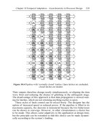
6.1.2 XScale Micro-architecture Overview
The XScale block diagram comprises Figure 6.1. The processor uses a
seven-stage (eight-stage cache access) pipeline [1]. The pipeline depth,
which at the time was more than usual for an embedded processor, allows
higher performance at low V
DD
, by shifting the maximum operating
frequency (F
max
) curve upward at all voltages. To support a wide range of
operating voltages, as well as DVS, two separate timing databases were
constructed as part of the performance validation. One was at the nominal
target V
DD
of 1.3 V and one was at 0.7 V. The low V
DD
timing database
allowed specific circuits, whose performance scaled poorly with reduced
voltage, to be identified, and appropriate design changes to be made.
Figure 6.1 The 180 nm XScale microprocessor micro-architecture. The PMU is
accessed through the coprocessor (CP14) interface. Frequency and V
DD
controls
reside in the CP15 configuration registers.
In particular, the differential cascade voltage-switched logic (DCVSL)
circuit style was often problematic at low V
DD
. DCVSL has poor delay vs.
V
DD
scaling properties due to its ratioed nature, where the input pull down
transistors must overpower the cross-coupled PMOS load transistors.
DCVSL was also incompatible with the static timing analysis tool and
therefore required increased engineering effort. Pulse-clocked latches
replaced master-slave latches in much of the design. These allowed about a
45% decrease in the sequential circuit energy per clock and reduced the
path delays due to sequential elements.
126 Lawrence T. Clark, Franco Ricci, William E. Brown
6.1.3 Dynamic Voltage Scaling
DVS scales the processor performance by adjusting the frequency at which
the processor operates to an estimate of the future workload. Scaling
frequency down delivers a linear power savings, while simultaneously
scaling V
DD
with the frequency changes allows quadratically reduced
power dissipation, which is compounded with the linear power dissipation
savings due to reduced operating frequency. On the 180 nm XScale, the
maximum operating frequency (F
max
) at each V
DD
scales with V
DD
1.75
as
shown in Figure 6.2. The actual F
max
vs. V
DD
behavior in the figure differs
from the ideal V
2
since the submicron transistors are velocity saturated,
and interconnect RC has an impact. Transistor currents scale at a reduced
exponent [5], while metal RC is constant with V
DD
. The net result is an
approximately cubic reduction in power dissipation, as shown in Figure 6.2.
Note that the F
max
approaches 0 MHz at a V
DD
greater than 0 V.
Figure 6.2 80200 XScale processor power dissipation vs. operating frequency
with constant V
DD
(dashed line) and scaled V
DD
(solid line) at the F
max
for each
voltage. The savings due to DVS is also shown.
Chapter 6 Dynamic Voltage Scaling with the XScale Embedded Microprocessor 127
CPUs on modern semiconductor fabrication processes dissipate a
considerable portion of their power from transistor-leakage currents [6].
Process scaling into the deep submicron region has resulted in exponential
increases in leakage currents. Reducing V
DD
scales these leakage
components more rapidly than even the V
2
dependency of the active power
component. Consequently, V
DD
scaling is also desirable in managing
leakage power dissipation and will become more so in the future [7].
When operating with DVS, the future workload must be estimated by
the OS from present operations and hints about future needs. The key is to
avoid missed deadlines, i.e., when scaling back the processor performance
to reduce the system power usage, the required tasks should still finish in
time. Examples of tasks that have deadlines are MPEG or audio decode
and playback, where each block must be delivered in time to the screen or
speakers. If a block is decoded late, the user experience suffers. Ideally,
the OS schedules tasks so that the processor is kept continually busy, i.e.,
there is no idle time, but so that no deadlines are missed. In reality, there is
always some idle time, since the scheduling must avoid degrading the user
experience, so the power savings is not as high as the ideal case. It is also
important to maintain the overall system responsiveness.
The XScale microprocessor PMU is critical to effective DVS use. The
PMU allows real-time determination of not just whether tasks are keeping
the processor busy, but whether they are being executed efficiently.
6.1.4 The Performance Measurement Unit
A performance measurement capability is necessary to effectively use
DVS in practical applications. Since the actual mix of applications and
their interaction with the OS cannot be known a priori, whether or not the
processor is running efficiently must be measured in real time. This
application mix-dependent behavior implies the need for some form of
hardware counting support to minimize power dissipation while ensuring
adequate quality of service. The additional hardware allows the OS to
estimate the future workload from the present one, ideally with hints from
the applications about priorities [3].
The XScale micro-architecture includes a performance measurement
unit (PMU) [8, 9] that supports this need. The monitors are accessed
through coprocessor registers (specifically CP14). The basic counting
mechanism is provided by a dedicated 32-bit clock counter and two
programmable 32-bit performance counters, PMN0 and PMN1. The
counters can trigger interrupts on rollovers under software control. The
performance monitor control register (PMNC) controls the monitored
events, resets counters, determines which counters have events, and
128 Lawrence T. Clark, Franco Ricci, William E. Brown
enables and disables interrupts. Table 6.1 lists the events that can be
monitored by the XScale PMU.
Table 6.1 Performance monitoring events supported by the XScale PMU [8]. The
numbers refer to the counters as chosen by the CP14 enables.
0 Instruction cache miss caused external memory access
1 Instruction not delivered by I-cache—I-cache or I-TLB miss
2 Data dependency stall
3 I-TLB miss
4 D-TLB miss
5 Branch instruction executed
6 Mispredicted branch
7 Instruction executed
8 Stall due to full data cache buffers (once per clock cycle)
9 Stall due to full data cache buffers (once per stall sequence)
10 D-cache access
11 D-cache miss
12 D-cache write back (for each four words written back)
13 Software-controlled PC change with no mode change
16 Bus memory request from core
17 Bus memory request queue full
18 Bus queues drained
20 Unlogged bus ECC error
21 Single-bit bus error
22 ECC required read–modify–write cycle for narrow write
The performance monitors can be used to determine the number of
actual clocks per instruction (CPI), bus activity, translation lookaside
buffer (TLB), and cache efficiency, for the code being run. The latter are
determined easily by counting TLB or cache misses. The performance
counters can also be used to determine average fetch latency, by counting
the stall cycles waiting for memory.
For DVS applications, the PMU is used to distinguish intervals where
the processor is continually busy, i.e., those where there is no idle time, vs.
those where it is actually accomplishing useful work. Consider an
application that is memory bandwidth limited. In this case, if the working
set does not fit in the D-cache, there is no idle time between tasks, but a
significant amount of the processor cycles are spent with the pipeline
stalled and waiting for bus operations, resulting in a high number of clocks
per instruction (CPI). In this case, lowering the voltage and frequency can
provide significant power savings with no impact on performance. When
the processor is running at a lower core voltage and frequency, there are
fewer stall cycles and hence a lower CPI.