Adaptive Techniques for Dynamic Processor Optimization_Theory and Practice Episode 2 Part 3 potx
Bạn đang xem bản rút gọn của tài liệu. Xem và tải ngay bản đầy đủ của tài liệu tại đây (677.83 KB, 20 trang )
190 Shidhartha Das, David Roberts, David Blaauw, David Bull, Trevor Mudge
Error signals of individual RFFs are OR-ed together to generate the
pipeline restore signal which overwrites the shadow latch data into the
main flip-flop, thereby restoring correct state in the cycle following the er-
roneous cycle. Thus, an erroneous instruction is guaranteed to recover with
a single cycle penalty, without having to be re-executed. This ensures that
forward progress in the pipeline is always maintained. Even if every in-
struction fails to meet timing, the pipeline still completes, albeit at a slower
speed. Upon detection of a timing error, a micro-architectural recovery
technique is engaged to restore the whole pipeline to its correct state.
8.4.2 Micro-architectural Recovery
The pipeline error recovery mechanism must guarantee that, in the pres-
ence of Razor errors, register and memory state is not corrupted with an
incorrect value. In this section, we highlight two possible approaches to
implementing pipeline error recovery. The first is a simple but slow
method based on clock-gating, while the second method is a much more
scalable technique based on counter-flow pipelining [29].
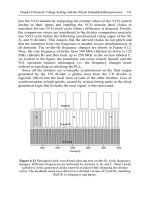
8.4.2.1 Recovery Using Clock-Gating
In the event that any stage detects a Razor error, the entire pipeline is
stalled for one cycle by gating the next global clock edge, as shown in
Figure 8.7(a). The additional clock period allows every stage to recompute
its result using the Razor shadow latch as input. Consequently, any previ-
ously forwarded erroneous values will be replaced with the correct value
from the Razor shadow latch, thereby guaranteeing forward progress. If all
stages produce an error each cycle, the pipeline will continue to run, but at
half the normal speed. To ensure negligible probability of failure due to
metastability, there must be two non-speculative stages between the last
Razor latch and the writeback (WB) stage. Since memory accesses to the
data cache are non-speculative in our design, only one additional stage la-
beled ST (stabilize) is required before writeback (WB). In the general case,
processors are likely to have critical memory accesses, especially on the
read path. Hence, the memory sub-system needs to be suitably designed
such that it can handle potentially critical read operations.
being metastable, before being written to memory. In our design, data ac-
cesses in the memory stage were non-critical and hence we required only
one additional pipeline stage to act as a dummy stabilization stage.
Chapter 8 Architectural Techniques for Adaptive Computing 191
8.4.2.2 Recovery Using Counter-Flow Pipelining
In aggressively clocked designs, it may not be possible to implement sin-
gle cycle, global clock-gating without significantly impacting processor
cycle time. Consequently, we have designed and implemented a fully pipe-
lined error recovery mechanism based on counter-flow pipelining tech-
niques [29]. The approach illustrated in Figure 8.7(b) places negligible
timing constraints on the baseline pipeline design at the expense of extend-
ing pipeline recovery over a few cycles. When a Razor error is detected,
two specific actions must be taken. First, the erroneous stage computation
following the failing Razor latch must be nullified. This action is accom-
plished using the bubble signal, which indicates to the next and subsequent
stages that the pipeline slot is empty. Second, the flush train is triggered by
asserting the stage ID of failing stage. In the following cycle, the correct
value from the Razor shadow latch data is injected back into the pipeline,
allowing the erroneous instruction to continue with its correct inputs. Ad-
ditionally, the flush train begins propagating the ID of the failing stage in
the opposite direction of instructions. When the flush ID reaches the start
of the pipeline, the flush control logic restarts the pipeline at the instruction
following the erroneous instruction.
Figure 8.7 Micro-architectural recovery schemes. (a) Centralized scheme
based on clock-gating. (b) Distributed scheme based on pipeline flush.
(
© IEEE 2005
)
IF
Razor FF
ID
Razor FF
EX
Razor FF
MEM
error
recover
recover recover
Razor FF
PC
recover
error
error
error
clock
recover
IF
Razor FF
ID
Razor FF
EX
Razor FF
MEM
(read-only)
WB
(reg/mem)
error bubble
recover recover
Razor FF
Stabilizer FF
PC
recover
flushID
bubble
error bubble
flushID
error bubble
flushID
Flush
Control
flushID
error
WB
(reg/mem)
Stabilizer FF
a)
b)
IF
Razor FFRazor FF
ID
Razor FFRazor FF
EX
Razor FF
MEM
error
recover
recover recover
Razor FF
PCPC
recover
error
error
error
clock
recover
IF
Razor FFRazor FF
ID
Razor FFRazor FF
EX
Razor FFRazor FF
MEM
(read-only)
WB
(reg/mem)
error bubble
recover recover
Razor FFRazor FF
Stabilizer FFStabilizer FF
PCPC
recover
flushID
bubble
error bubble
flushID
error bubble
flushID
Flush
Control
flushID
error
WB
(reg/mem)
Stabilizer FFStabilizer FF
a)
b)
192 Shidhartha Das, David Roberts, David Blaauw, David Bull, Trevor Mudge
8.4.3 Short-Path Constraints
The duration of the positive clock phase, when the shadow latch is trans-
parent, determines the sampling delay of the shadow latch. This constrains
the minimum propagation delay for a combinational logic path terminating
in a RFF to be at least greater than the duration of the positive clock phase
and the hold time of the shadow latch. Figure 8.8 conceptually illustrates
this minimum delay constraint. When the RFF input violates this constraint
and changes state before the negative edge of the clock, it corrupts the
state of the shadow latch. Delay buffers are required to be inserted in those
paths which fail to meet this minimum path delay constraint imposed by
the shadow latch.
The shadow latch sampling delay represents the trade-off between the
power overhead of delay buffers and the voltage margin available for Ra-
zor sub-critical mode of operation. A larger value of the sampling delay al-
lows greater voltage scaling headroom at the expense of more delay buff-
ers and vice versa. However, since Razor protection is only required on the
critical paths, overhead due to Razor is not significant. On the Razor proto-
type subsequently presented, the power overhead due to Razor was less
than 3% of the nominal power overhead.
8.4.4 Circuit-Level Implementation Issues
Figure 8.9 shows the transistor level schematic of the RFF. The error com-
parator is a semi-dynamic XOR gate which evaluates when the data
latched by the slave differs from that of the shadow in the negative clock
phase. The error comparator shares its dynamic node, Err_dyn, with the
metastability detector which evaluates in the positive phase of the clock
when the slave output could become metastable. Thus, the RFF error sig-
nal is flagged when either the metastability detector or the error compara-
tor evaluates.
Launch clock
T
hold
Min. path delay
Min. Path Delay > t
spec
+ t
hold
intended path
short path
T
spec
Capture clock
Launch clock
T
hold
Min. path delay
Min. Path Delay > t
spec
+ t
hold
intended path
short path
T
spec
Capture clock
Fi
g
ure 8.8 Shor
t
-
p
ath constraints.
Chapter 8 Architectural Techniques for Adaptive Computing 193
This, in turn, evaluates the dynamic gate to generate the restore signal
by “OR”-ing together the error signals of individual RFFs (Figure 8.10), in
the negative clock phase. The restore needs to be latched at the output of
the dynamic OR gate so that it retains state during the next positive phase
(recovery cycle) during which it disables the shadow latch to protect state.
The shadow latch can be designed using weaker devices since it is required
only for runtime validation of the main flip-flop data and does not form a
part of the critical path of the RFF.
The rbar_latched signal, shown in the restore generation circuitry in
Figure 8.10, which is the half-cycle delayed and complemented version of
Figure 8.10 Restore generation circuitry. (© IEEE 2005)
ERROR 0
ERROR 63
CLK_n
CLK_n
CLK_n
CLK_p
Q
LATCH1
RBAR_LATCHED
RESTORE
Q_n
LATCH2
CLK
CLK_pCLK_n
P-SKEWED FF
N-SKEWED FF
FAIL
FFP1 FFP2
FFN1 FFN2
ERROR 0
ERROR 63
CLK_n
CLK_n
CLK_n
CLK_p
Q
LATCH1
RBAR_LATCHED
RESTORE
Q_n
LATCH2
CLK
CLK_pCLK_n
P-SKEWED FF
N-SKEWED FF
FAIL
FFP1 FFP2
FFN1 FFN2
SH
SH
QS
QS
P-SKEWED
N-SKEWED
RBAR_LATCHED
ERR_DYN
ERROR
CLK
CLK
RESTORE
CLK
CLK
CLK
CLK
RESTORE
CLK
CLK
RESTORE
CLK
PS
PS
NS
NS
CLK
SL
SL
SH
SH
PS
PS
NS
NS
ERROR COMPARATOR
METASTABILITY DETECTORSHADOW LATCH
MASTER LATCH
SLAVE LATCH
D
Q
Q
G1
SH
SH
QS
QS
P-SKEWED
N-SKEWED
RBAR_LATCHED
ERR_DYN
ERROR
CLK
CLK
RESTORE
CLK
CLK
CLK
CLK
RESTORE
CLK
CLK
RESTORE
CLK
PS
PS
NS
NS
CLK
SL
SL
SH
SH
PS
PS
NS
NS
ERROR COMPARATOR
METASTABILITY DETECTORSHADOW LATCH
MASTER LATCH
SLAVE LATCH
D
Q
Q
G1
Figure 8.9 Razor flip-flop circuit schematic. (© IEEE 2005)
194 Shidhartha Das, David Roberts, David Blaauw, David Bull, Trevor Mudge
the restore signal, precharges the Err_dyn node for the next errant cycle.
Thus, unlike standard dynamic gates where precharge takes place every
cycle, the Err_dyn node is conditionally precharged in the recovery cycle
following a Razor error.
Compared to a regular DFF of the same drive strength and delay, the
RFF consumes 22% extra (60fJ/49fJ) energy when sampled data is static
and 65% extra (205fJ/124fJ) energy when data switches. However, in the
processor, only 207 flip-flops out of 2388 flip-flops, or 9%, could become
critical and needed to be RFFs. The Razor power overhead was computed
to be 3% of nominal chip power.
The metastability detector consists of p- and n-skewed inverters which
switch to opposite power rails under a metastable input voltage. The detec-
tor evaluates when input node SL can be ambiguously interpreted by its
fan-out, inverter G1 and the error comparator. The DC transfer curve
(Figure 8.11a) of inverter G1, the error comparator and the metastability
detector show that the “detection” band is contained well within the am-
biguously interpreted voltage band. Figure 8.11(b) gives the error detection
and ambiguous interpretation bands for different corners. The probability
that metastability propagates through the error detection logic and causes
metastability of the restore signal itself was computed to be below 2e-30
[30]. Such an event is flagged by the fail signal generated using double-
skewed flip-flops. In the rare event of a fail, the pipeline is flushed and the
supply voltage is immediately increased.
Figure 8.11 Metastability detector characteristics. (a) Principle of
operation. (b) Metastability detector: corner analysis. (© IEEE 2005)
0.58-0.890.64-0.8127C1.8VFast
0.65-0.900.71-0.8340C1.8VTyp.
0.67-0.930.77-0.8785C1.8VSlow
0.40-0.610.48-0.5627C1.2VFast
0.48-0.610.52-0.5840C1.2VTyp.
0.53-0.640.57-0.6085C1.2VSlow
TEMPVDDProc
Detection
Band
Ambiguous
Band
Corner
0.58-0.890.64-0.8127C1.8VFast
0.65-0.900.71-0.8340C1.8VTyp.
0.67-0.930.77-0.8785C1.8VSlow
0.40-0.610.48-0.5627C1.2VFast
0.48-0.610.52-0.5840C1.2VTyp.
0.53-0.640.57-0.6085C1.2VSlow
TEMPVDDProc
Detection
Band
Ambiguous
Band
Corner
0.00.40.81.21.62.0
0.0
0.4
0.8
1.2
1.6
Error Comparator
Driver G1
Metastability
Detector
Voltage of Node QS
V_OUT
Detection Band
Ambiguous Band
DC Transfer Characteristics
0.00.40.81.21.62.0
0.0
0.4
0.8
1.2
1.6
Error Comparator
Driver G1
Metastability
Detector
Voltage of Node QS
V_OUT
Detection Band
Ambiguous Band
DC Transfer Characteristics
a) b)
Chapter 8 Architectural Techniques for Adaptive Computing 195
8.5 Silicon Implementation and Evaluation of Razor
A 64b processor which implements a subset of the Alpha instruction set was
designed and built as an evaluation vehicle for the concept of Razor. The
chip was fabricated with MOSIS [31] in an industrial 0.18 micron technol-
ogy. Voltage control is based on the observed error rate and power savings
are achieved by (1) eliminating the safety margins under nominal operating
and silicon conditions and (2) scaling voltage 120mV below the first failure
point to achieve a 0.1% targeted error rate. It was tested and measured for
savings due to Razor DVS for 33 different dies from two different lots and
obtained an average energy savings of 50% over the worst-case operating
conditions by operating at the 0.1% error rate voltage at 120MHz. The proc-
essor core is a five-stage in-order pipeline which implements a subset of the
Alpha instruction set. The timing critical stages of the processor are the In-
struction Decode (ID) and the Execute (EX) stages. The distributed pipeline
recovery scheme as illustrated in Figure 8.7(b) was implemented. The die
photograph of the processor is shown in Figure 8.12(a), and the relevant im-
plementation details are provided in Figure 8.12(b).
Figure 8.12 Silicon evaluation of Razor. (a) Die micrograph. (b) Processor
im
p
lementation details.
(
© IEEE 2005
)
3.7mWTotal Delay Buffer Power
Overhead
2.9%% Total Chip Power Overhead
Error Correction and Recovery Overhead
260fJEnergy of a RFF per error event
60fJ/205fJRFF Energy (Static/Switching)
49fJ/124fJStandard FF Energy
(Static/Switching)
Error Free Operation (Simulation Results)
2801Number of Delay Buffers Added
207Total Number of Razor Flip-Flops
2388Total Number of Flip-Flops
8KBDcache Size
8KBIcache Size
130mWMeasured Chip Power at 1.8V
3.3mm*3.6
mm
Die Size
1.58millionTotal Number of Transistors
1.2-1.8VDVS Supply Voltage Range
140MHzMax. Clock Frequency
0.18µmTechnology Node
a) b)
196 Shidhartha Das, David Roberts, David Blaauw, David Bull, Trevor Mudge
8.5.1 Measurement Results
Figure 8.13 shows the error rates and normalized energy savings versus
supply voltage at 120 and 140MHz for one of the 33 chips tested, hence-
forth referred to as chip1. Energy at a particular voltage is normalized with
respect to the energy at the point of first failure. For all plotted points, cor-
rect program execution with Razor was verified. The Y-axis on the left
shows the percentage error rate and that on the right shows the normalized
energy of the processor.
From the figure, we note that the error rate at the point of first failure is
very low and is of the order of 1.0e-7. At this voltage, a few critical paths
that are rarely sensitized fail to meet setup requirements and are flagged as
timing errors. As voltage is scaled further into the sub-critical regime, the
error rate increases exponentially. The IPC penalty due to the error recov-
ery cycles is negligible for error rates below 0.1%. Under such low error
rates, the recovery overhead energy is also negligible and the total proces-
sor energy shows a quadratic reduction with the supply voltage. At error
rates exceeding 0.1%, the recovery energy rapidly starts to dominate, off-
setting the quadratic savings due to voltage scaling. For the measured
chips, the energy optimal error rate fell at approximately 0.1%.
The correlation between the first failure voltage and the 0.1% error rate
voltage is shown in the scatter plot of Figure 8.14. The 0.1% error rate volt-
age shows a net variation of 0.24V from 1.38V to 1.62V which is approxi-
mately 20% less than the variation observed for the voltage at the point of
Figure 8.13 Measured error rate and energy versus supply voltage. (© IEEE 2005)
1.52 1.56 1.60 1.64 1.68 1.72 1.76
0.70
0.75
0.80
0.85
0.90
0.95
1.00
1.05
1.10
1.15
1.20
1E-8
1E-7
1E-6
1E-5
1E-4
1E-3
0.01
0.1
1
10
120MHz
Normalized Energy
Percentage Error Rate
140MHz
Voltage (in Volts)
Chip 1
Point of First Failure
Sub-critical
Chapter 8 Architectural Techniques for Adaptive Computing 197
first failure. The relative “flatness” of the linear fit indicates less sensitivity
to process variation when running at a 0.1% error rate than at the point of
first failure. This implies that a Razor-enabled processor, designed to operate
at the energy optimal point, is likely to show greater predictability in terms
of performance than a conventional worst-case optimized design. The en-
ergy optimal point requires a significant number of paths to fail and statisti-
cally averages out the variations in path delay due to process variation, as
opposed to the first failure point which, being determined by the single long-
est critical path, shows higher process variation dependence.
8.5.2 Total Energy Savings with Razor
The total energy savings was measured by quantifying the savings due to
elimination of safety margins and operation in the sub-critical voltage re-
gime. Table 8.2 lists the measured voltage margins for process, voltage and
temperature uncertainties for 2 out of the 33 chips tested, when operating at
120MHz. The chips are labeled as chip 1 and chip 2, respectively. The first
failure voltage for chips 1 and 2 are 1.74V and 1.63V, respectively, and
hence represent slow and typical process conditions, respectively.
Table 8.2 Measurement of voltage safety margins.
Margins
Chip (point of first failure) Process Voltage Temperature
Slowest chip (1.76V)
0mV 180mV 100mV
Chip 1 (1.73V)
30mV 180mV 100mV
Chip 2 (1.63V)
130mV 180mV 100mV
Figure 8.14 Scatter plot showing the point of 0.1% error rate
versus the
p
oint of first failure.
(
© IEEE 2005
)
1.4 1.5 1.6 1.7 1.8
1.4
1.5
1.6
1.7
1.8
Chips
Linear Fit
y=0.8x + 0.2
Voltage at First Failure
Voltage at 0.1%Error Rate
1.5 1.6 1.7 1.8
1.4
1.5
1.6
1.7
1.8
Chips
(Linear Fit)
(0.6x + 0.6)
Voltage at 0.1%Error Rate
Voltage at First Failure
120MHz 140MHz
1.4 1.5 1.6 1.7 1.8
1.4
1.5
1.6
1.7
1.8
Chips
Linear Fit
y=0.8x + 0.2
Voltage at First Failure
Voltage at 0.1%Error Rate
1.5 1.6 1.7 1.8
1.4
1.5
1.6
1.7
1.8
Chips
(Linear Fit)
(0.6x + 0.6)
Voltage at 0.1%Error Rate
Voltage at First Failure
120MHz 140MHz
198 Shidhartha Das, David Roberts, David Blaauw, David Bull, Trevor Mudge
The point of first failure of the slowest chip at 25°C is 1.76V. For this
chip to operate correctly in the worst-case, voltage and temperature mar-
gins are added over and above the first failure voltage. The worst-case
temperature margin was measured as the shift in the point of first failure of
this chip when heated from 25°C to 10°5C. At 105°C, this chip fails at
1.86V, an increase of 100mV over the first failure voltage at 25°C. The
worst-case voltage margin was estimated to be 10% of the nominal supply
voltage of 1.8V (180mV). The margin for inter-die process variations was
measured as the difference in the point of first failure voltage of the chip
under test and the slowest chip. For example, chip 2 fails at 1.63V at 25°C
when compared with the slowest chip which fails at 1.76V. This translates
to 130mV process margin. Thus, with the incorporation of 100mV tem-
perature margin and 180mV voltage margin over the first failure point of
the slowest chip, the worst-case operating voltage for guaranteed correct
operation was obtained to be 2.04V.
Figure 8.15 lists the energy savings obtained through Razor for chips 1
and 2. The first set of bars shows the energy when Razor is turned off and
the chip under test is operated at the worst-case operating voltage at
120MHz, as determined for all the chips tested. At the worst-case voltage
of 2.04V, chip 2 consumes 160.5mW of which 27.3mW is due to 180mV
margin for supply voltage drop, 11.2mW is due to 100mV temperature
margin and 17.3mW is due to 30mV process margin.
Figure 8.15 Total energy savings. (© IEEE 2005)
80
100
120
140
160
27.3mW
180mV
Power
Supply
Integrity
11.3mW
70mV
Temp
17.3mW
130mV
Process
104.5mW
4.2mW
30mV
Process
89.7mW
99.6mW
104.5mW
119.4mW
89.7mW
119.4mW
11.5mW
70mV
Temp
27.7mW
180mV
Power
Supply
Integrity
104.5mW
119.4mW
99.6mW
chip2
chip1
chip2
chip1
chip2
chip1
Measured Power
with supply, temperature
and process margins
Power with Razor DVS
when Operating at Point
of First Failure
Power with Razor DVS
when Operating at Point
of 0.1% Error Rate
Measured Power (in mW)
160.5mW
162.8mW
Slight performance loss
at 0.1% error rate
Chapter 8 Architectural Techniques for Adaptive Computing 199
The second set of bars shows the energy when operating with Razor en-
abled at the point of first failure with all the safety margins eliminated. At
the point of first failure, chip 2 consumes 104.5mW, while chip 1 consumes
119.4mW of power. Thus, for chip 2, operating at the first failure point leads
to a saving of 56mW which translates to 35% saving over the worst case.
The corresponding saving for chip 1 is 27% over the worst case.
The third set of bars shows the additional energy savings due to sub-
critical mode of operation of Razor. With Razor enabled, both chips are op-
erated at the 0.1% error rate voltage and power measurements are taken. At
the 0.1% error rate, chip 1 consumes 99.6mW of power at 0.1% error rate
which is a saving of 39% over the worst case. When averaged over all die,
we obtain approximately 50% savings over the worst case at 120MHz and
45% savings at 140MHz when operating at the 0.1% error rate voltage.
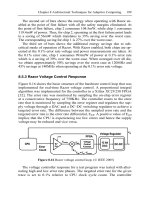
8.5.3 Razor Voltage Control Response
Figure 8.16 shows the basic structure of the hardware control loop that was
implemented for real-time Razor voltage control. A proportional integral
algorithm was implemented for the controller in a Xilinx XC2V250 FPGA
[32]. The error rate was monitored by sampling the on-chip error register
at a conservative frequency of 750KHz. The controller reacts to the error
rate that is monitored by sampling the error register and regulates the sup-
ply voltage through a DAC and a DC–DC switching regulator to achieve a
targeted error rate. The difference between the sampled error rate and the
targeted error rate is the error rate differential, E
diff
. A positive value of E
diff
implies that the CPU is experiencing too few errors and hence the supply
voltage may be reduced and vice versa.
Figure 8.16 Razor voltage control loop. (© IEEE 2005)
V
dd
CPU
Error
Count
Σ
E
ref
E
sample
E
diff
= E
ref
-E
sample
E
diff
12 bit
DAC
DC-DC
Voltage
Control
Function
Voltage Regulator
FPGA
reset
V
dd
CPU
Error
Count
ΣΣ
E
ref
E
sample
E
diff
= E
ref
-E
sample
E
diff
12 bit
DAC
DC-DC
Voltage
Control
Function
Voltage Regulator
FPGA
reset
The voltage controller response for a test program was tested with alter-
nating high and low error rate phases. The targeted error rate for the given
trace is set to 0.1% relative to CPU clock cycle count. The controller
200 Shidhartha Das, David Roberts, David Blaauw, David Bull, Trevor Mudge
rate phase is shown in Figure 8.17(a). Error rates increase to about 15% at
the onset of the high-error phase. The error rate falls until the controller
reaches a high enough voltage to meet the desired error rate in each milli-
second sample period. During a transition from the high-error rate phase to
the low-error rate phase, shown in Figure 8.17(b), the error rate drops to
zero because the supply voltage is higher than required. The controller re-
sponds by gradually reducing the voltage until the target error rate is
achieved.
8.6 Ongoing Razor Research
Currently, research efforts on Razor are underway in ARM Ltd, UK. A
deeper analysis of Razor as explained in the previous sections reveals sev-
eral key issues that need to be addressed, before Razor can be deployed as
mainstream technology.
The primary concern is the issue of Razor energy overhead. Since indus-
trial strength designs are typically balanced, it is likely that significantly
larger percentage of flip-flops will require Razor protection. Consequently,
a greater number of delay buffers will be required to satisfy the short-path
constraints. Increasing intra-die process variability, especially on the short
paths, further aggravates this issue.
Figure 8.17 Voltage controller phase transition response. (a) Low to high
transition. (b) High to low transition. (© IEEE 2005)
Percentage Error Rate
Controller Output Voltage(V)
Percentage Error Rate
Controller Output Voltage(V)
Time (s)
Time (s)
25.2 25.3 25.4 25.5
0
2
4
6
8
10
12
14
16
1.58
1.60
1.62
1.64
1.66
1.68
1.70
1.72
29.429.529.629.7
0.0
0.5
1.0
1.5
2.0
1.56
1.58
1.60
1.62
1.64
1.66
1.68
1.70
1.72
High to Low
Error-rate phase transition
Low to High
Error-rate phase transition
response during a transition from the lowerror rate phase to the high-error
Chapter 8 Architectural Techniques for Adaptive Computing 201
Another important concern is ensuring reliable state recovery in the
presence of timing errors. The current scheme imposes a massive fan-out
load on the pipeline restore signal. In addition, the current scheme cannot
recover from timing errors in critical control signals which can cause unde-
tectable state corruption in the shadow latch. Metastability on the restore
signal further complicates state recovery. Though such an event is flagged
by the fail signal, it makes validation and verification of a “Razor”-ized
processor extremely problematic in current ASIC design methodologies.
An attempt is made to address these concerns by developing an alterna-
tive scheme for Razor, henceforth referred to as Razor II. The key idea in
Razor II is to use the Razor flip-flop only for error detection. State recov-
ery after a timing error occurs by a conventional replay mechanism from a
check-pointed state. Figure 8.18 shows the pipeline modifications required
to support such a recovery mechanism. The architectural state of the proc-
essor is check-pointed when an instruction has been validated by Razor
and is ready to be committed to storage. The check-pointed state is buff-
ered from the timing critical pipeline stages by several stages of stabiliza-
tion which reduce the probability of metastability by effectively double-
latching the pipeline output. Upon detection of a Razor error, the pipeline
is flushed and system recovers by reverting back to the check-pointed ar-
chitectural state and normal execution is resumed. Replaying from the
Register
Bank,
PC,
PSR
Run-time
state
(Reg, PC,
PSR)
Razor Error
Control
Error
recover
IF
ID
EX
ME
WB
Stabilization
freq
Vdd
Clock
and
Voltage
Control
Check-pointed
State
Timing-critical pipeline stages
PC
RFF
RFF
RFF
RFF
Error
Detection
Error
Detection
Error
Detection
Error
Detection
Error
Detection
Synchronization
flops
flush
RFF
Figure 8.18 Pipeline modifications required for Razor II.
202 Shidhartha Das, David Roberts, David Blaauw, David Bull, Trevor Mudge
check-pointed state implies that a single instruction can fail in successive
roll-back cycles, thereby leading to a deadlock. Forward progress in such a
system is guaranteed by detecting a repeatedly failing instruction and exe-
cuting the system at half the nominal frequency during recovery.
Error detection in Razor II is based on detecting spurious transitions in the
D-input of the Razor flip-flop, as conceptually illustrated in Figure 8.19. The
duration where the input to the RFF is monitored for errors is called the
detection window. The detection window covers the entire positive phase
of the clock cycle. In addition, it also includes the setup window in front of
the positive edge of the clock. Thus, any transition in the setup window is
suitably detected and flagged. In order to reliably flag potentially metasta-
ble events, safety margin is required to be added to the onset of the detec-
tion window. This ensures that the detection window covers the setup win-
dow under all process, voltage and temperature conditions. In a recent
work, the authors have applied the above concept to detect and correct
transient single event upset failures [33].
8.7 Conclusion
As process variations increase with each technology generation, adap-
tive techniques assume even greater relevance. However, deploying such
techniques in the field is hindered either by their complexity as in the case
Figure 8.19 Transition detection-based error detection.
T
setup
T
pos
Clock
Data
Error
T
margin
Detection Window
T
setup
T
pos
Clock
Data
Error
T
margin
Detection Window
In this chapter, we presented a survey of different adaptive techniques re-
ported in literature. We analyzed the concept of design margining in the
presence of process variations and looked at how different adaptive tech-
niques help eliminate some of the margins. We categorized these techniques
as “always-correct” and “error detection and correction” techniques. We
presented Razor as a special case study of the latter category and showed
silicon measurement results on a chip using Razor for supply voltage
control.
Chapter 8 Architectural Techniques for Adaptive Computing 203
of Razor or by the lack of substantial gains as in the case of canary cir-
cuits. Future research in this field needs to focus on combining effective-
ness of Razor in eliminating design margins with the relative simplicity of
the “always-correct” techniques. As uncertainties worsen, adaptive tech-
niques provide a solution toward achieving computational correctness and
faster design closure.
References
[1] S.T. Ma, A. Keshavarzi, V. De, J.R. Brews, “A statistical model for extract-
ing geometric sources of transistor performance variation,” IEEE Transac-
tions on Electron Devices, Volume 51, Issue 1, pp. 36–41, January 2004.
[3] S. Yokogawa, H. Takizawa, “Electromigration induced incubation, drift and
threshold in single-damascene copper interconnects,” IEEE 2002 Interna-
tional Interconnect Technology Conference, 2002, pp. 127–129, 3–5 June
2002.
[4] W. Jie and E. Rosenbaum, “Gate oxide reliability under ESD-like pulse
stress,” IEEE Transactions on Electron Devices, Volume 51, Issue 7, July
2004.
[5] International Technology Roadmap for Semiconductors, 2005 edition,
Links/2005ITRS/Home2005.htm.
[6] M. Hashimoto, H. Onodera, “Increase in delay uncertainty by performance
optimization,” IEEE International Symposium on Circuits and Systems,
2001, Volume 5, pp. 379–382, 5, 6–9 May 2001.
[8] G. Wolrich, E. McLellan, L. Harada, J. Montanaro, and R. Yodlowski, “A
high performance floating point coprocessor,” IEEE Journal of Solid-State
Circuits, Volume 19, Issue 5, October 1984.
[9] Trasmeta Corporation, “LongRun Power Management,” ns-
meta.com/tech/longrun2.html
[11] ARM Limited,
[12] T. Burd, T. Pering, A. Stratakos, and R. Brodersen, “A dynamic voltage
scaled microprocessor system,” International Solid-State Circuits Confer-
ence, February 2000.
[13] A.K. Uht, “Going beyond worst-case specs with TEATime,” IEEE Micro
Top Picks, pp. 51–56, 2004
[2] R. Gonzalez, B. Gordon, and M. Horowitz, “Supply and threshold voltage
scaling for low power CMOS,” IEEE Journal of Solid-State Circuits,
Volume 32, Issue 8, August 1997.
[7] S. Rangan, N. Mielke and E. Yeh, “Universal recovery behavior of negative
bias temperature instability,” IEEE Intl. Electron Devices Mtg., p. 341,
December 2003.
[10] Intel Corporation, “Intel Speedstep Technology,” />port/processors/mobile/pentiumiii/ss.htm
204 Shidhartha Das, David Roberts, David Blaauw, David Bull, Trevor Mudge
[15] T.D. Burd, T.A. Pering, A.J. Stratakos and R.W. Brodersen, “A dynamic
voltage scaled microprocessor system,” IEEE Journal of Solid-State Circuits,
Volume 35, Issue 11, pp. 1571–1580, November 2000
[16] Berkeley Wireless Research Center,
[17] M. Nakai, S. Akui, K. Seno, T. Meguro, T. Seki, T. Kondo, A. Hashiguchi,
H. Kawahara, K. Kumano and M. Shimura, “Dynamic voltage and frequency
management for a low power embedded microprocessor,” IEEE Journal of
Solid-State Circuits, Volume 40, Issue 1, pp. 28–35, January. 2005
[19] T. Kehl, “Hardware self-tuning and circuit performance monitoring,” 1993
Int’l Conference on Computer Design (ICCD-93), October 1993.
[20] S. Lu, “Speeding up processing with approximation circuits,” IEEE Micro
Top Picks, pp. 67–73, 2004
[21] T. Austin, V. Bertacco, D. Blaauw and T. Mudge, “Opportunities and chal-
lenges in better than worst-case design,” Proceedings of the ASP-DAC 2005,
Volume 1, pp. 18–21, 2005.
[22] C. Kim, D. Burger and S.W. Keckler, IEEE Micro, Volume 23, Issue 6, pp.
99–107, November–December 2003.
[23] Z. Chishti, M.D. Powell, T. N. Vijaykumar, “Distance associativity for high-
performance energy-efficient non-uniform cache architectures,” Proceedings
of the International Symposium on Microarchitecture, 2003, MICRO-36
[24] F. Worm, P. Ienne and P. Thiran, “A robust self-calibrating transmission
scheme for on-chip networks,” IEEE Transactions on Very Large Scale Inte-
gration, Volume 13, Issue 1, January 2005.
[25] R. Hegde and N. R. Shanbhag, “A voltage overscaled low-power digital fil-
ter IC,” IEEE Journal of Solid-State Circuits, Volume39, Issue 2, February
2004.
[26] D. Roberts, T. Austin, D. Blaauw, T. Mudge and K. Flautner, “Error analysis
for the support of robust voltage scaling,” International Symposium on Qual-
ity Electronic Design (ISQED), 2005.
[27] L. Anghel and M. Nicolaidis, “Cost reduction and evaluation of a temporary
faults detecting technique,” Proceedings of Design, Automation and Test in
Europe Conference and Exhibition 2000, 27–30 March 2000 pp. 591–598
[28] S. Das, D. Roberts, S. Lee, S. Pant, D. Blaauw, T. Austin, T. Mudge,
K. Flautner, “A self-tuning DVS processor using delay-error detection and
correction,” IEEE Journal of Solid-State Circuits, pp. 792–804, April 2006.
[14] K.J. Nowka, G.D. Carpenter, E.W. MacDonald, H.C. Ngo, B.C Brock,
K.I. Ishii, T.Y. Nguyen and J.L. Burns, “A 32-bit powerPC system-on-a-chip
with support for dynamic voltage scaling and dynamic frequency scaling,”
IEEE Journal of Solid-State Circuits, Volume 37, Issue 11, pp. 1441–1447,
November 2002
[18] A. Drake, R. Senger, H. Deogun, G. Carpenter, S. Ghiasi, T. Ngyugen,
N. James and M. Floyd, “A distributed critical-path timing monitor for a
65nm high-performance microprocessor,” International Solid-State Circuits
Conference, pp. 398–399, 2007.
Chapter 8 Architectural Techniques for Adaptive Computing 205
[29] R. Sproull, I. Sutherland, and C. Molnar, “Counterflow pipeline processor
architecture,” Sun Microsystems Laboratories Inc. Technical Report SMLI-
TR-94-25, April 1994.
[30] W. Dally, J. Poulton, Digital System Engineering, Cambridge University
Press, 1998
[31] www.mosis.org
[32] www.xilinx.com
[33] D. Blaauw, S.Kalaiselvam, K. Lai, W.Ma, S. Pant, C. Tokunaga, S. Das and
D.Bull “RazorII: In-situ error detection and correction for PVT and SER tol-
erance,” International Solid-State Circuits Conference, 2008
[34] D. Ernst, N. S. Kim, S. Das, S. Pant, T. Pham, R. Rao, C. Ziesler, D. Blaauw,
T. Austin, T. Mudge, K. Flautner, “Razor: A low-power pipeline based on
circuit-level timing speculation,” Proceedings of the 36th Annual
IEEE/ACM International Symposium on Microarchitecture, pp. 7–18, De-
cember 2003.
[35] A. Asenov, S. Kaya, A.R. Brown, “Intrinsic parameter fluctuations in de-
cananometer MOSFETs introduced by gate line edge roughness,” IEEE
Transactions on Electron Devices, Volume 50, Issue 5, pp. 1254–1260, May
2003.
[36] K. Ogata, “Modern control engineering,” 4th edition, Prentice Hall,
New Jersey, 2002.
Chapter 9 Variability-Aware Frequency Scaling
Sebastian Herbert, Diana Marculescu
Carnegie Mellon University
9.1 Introduction
Variability is becoming a key concern for microarchitects as technology
scaling continues and more and more increasingly ill-defined transistors
are placed on each die. Process variations during fabrication result in a
nonuniformity of transistor delays across a single die, which is then
compounded by dynamic thermally dependent delay variation at runtime.
The delay of every critical path in a synchronously timed block must be
less than the proposed cycle time for the block as a whole to meet that
timing constraint. Thus, as both the amount of variation (due to ever-
shrinking feature sizes as well as greater temperature gradients) and the
number of critical paths (due to increasing design complexity and levels of
integration) grow, the reduction in clock speed necessary to reduce the
probability of a timing violation to an acceptably small level increases.
However, the worst-case delay is very rarely exercised, and as a result, the
overdesign that is necessary to deal with variability sacrifices large
amounts of performance in the common case. Bowman et al. found that
designs for the 50 nm technology node could lose an entire generation’s
worth of performance due to systematic within-die process variability
alone [2].
A variability-aware microarchitecture is able to recover some of this
lost performance. One such microarchitecture partitions a processor into
multiple independently clocked frequency islands (FIs) [10, 14] and then
uses this partitioning to address variations at the clock domain granularity.
This chapter is an extension of the analysis of this microarchitecture
performed by Herbert et al. [7].
in Multi-Clock Processors
A. Wang, S. Naffziger (eds.), Adaptive Techniques for Dynamic Processor Optimization,
DOI: 10.1007/978-0-387-76472-6_9, © Springer Science+Business Media, LLC 2008
208 Sebastian Herbert, Diana Marculescu
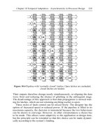
Figure 9.1 A microprocessor design using frequency islands.
Multi-clock designs using frequency islands provide increased
flexibility over globally clocked designs. Each frequency island operates
synchronously using its own local clock signal. However, arbitrary clock
ratios are allowed between any pair of frequency islands, necessitating the
use of asynchronous interfacing circuitry for inter-domain communication.
For this reason, designs using frequency islands are often referred to as
globally asynchronous, locally synchronous (GALS) designs.
An example of a frequency island design is shown in Figure 9.1. The
processor core is divided into five clock domains. One contains the front-
end fetch and decode logic, a second contains the register file, reorder
buffer, and register renaming logic, and the execution units are split into
integer, floating point, and memory domains. All communication between
the domains must be synchronized by passing through a dual-clock FIFO.
Performing variability-aware frequency scaling using the FI partitioning
addresses two sources of variability. First, it reduces the impact of random
within-die process variability. As noted above, the probability of meeting a
given timing constraint t
max
decreases with both the amount of variability
and the number of critical paths. While the amount of process variation
cannot be addressed at the microarchitecture level, microarchitects can
exercise some control over how often and where critical paths will be
found.
Chapter 9 Variability-Aware Frequency Scaling in Multi-Clock Processors 209
Second, it addresses dynamic thermal variability that manifests itself as
hotspots across the surface of the microprocessor die. At typical operating
temperatures, transistor delay increases with temperature as a result of the
effect of temperature on carrier mobility. Once again, an entire
synchronously timed block must be clocked such that the delay through its
hottest part meets its timing constraint, even though cooler parts could be
run faster without creating local timing violations. If a microarchitecture
has no thermal awareness, it is limited to always running at the frequency
that results in correct operation at the maximum specified operating
temperature.
Variability-aware frequency scaling (VAFS) sets the frequency of each
clock domain as high as possible given that domain’s worst local
variations, rather than slowing down the entire processor to compensate for
the worst global variations. Each clock domain in the FI processor has
fewer critical paths than the processor as a whole, which shifts the mean of
the maximum frequency distribution for each domain higher. Thus, the
domains in the FI version can, on average, be clocked faster than the
synchronous baseline to some degree, recovering some of the performance
lost to process variation. This is a result of the fact that in the FI case, each
clock domain’s frequency is limited by its slowest local critical path rather
than by the global slowest critical path, as in the fully synchronous case.
Thermal variability is addressed in a similar manner. In the synchronous
case, the entire core must be slowed down to accommodate the
temperature-induced increase in delay through its hottest block. For the FI
case, the same is only true at the clock domain granularity. Thus, the
impact of a hotspot on timing is isolated to the domain it is located in and
does not require a global reduction in clock frequency.
9.2 Addressing Process Variability
9.2.1 Approach
The impact of parameter variations has been extensively studied at the
circuit and device levels. However, with the increasing impact of
variability on design yield, it has become essential to consider higher level
models for parameter variation. Bowman et al. introduced the FMAX
model with the aim of quantifying the impact of die-to-die and within-die
variations on overall timing yield [2, 3]. They showed that the impact of
variability on combinational circuits can be captured using two parameters:
the logic depth of the circuit n
cp
and the number of independent critical
210 Sebastian Herbert, Diana Marculescu
paths in the circuit N
cp
. They observed that within-die (WID) variations
tend to determine the mean of the worst-case delay distribution of a circuit,
while die-to-die (D2D) variability determines its variance. Their model
was validated against microprocessors from 0.25 μm to 0.13 μm
technology nodes and was shown to accurately predict the mean, variance,
and shape of the maximum frequency distribution. The FMAX model has
subsequently been used in many studies on the effects of process variations
at the microarchitecture level [9, 11, 12].
Typical microprocessor designs attempt to balance the logic depth
across stages, so the number of critical paths N
cp
is the dominant factor in
determining the differences in how process variability affects each
microarchitectural block. The delays of the N
cp
independent critical paths
are modeled as independent, identically distributed normal
()
2
,
,
cp nom WID
T
σ
random variables with probability density function (PDF) f
WID
(t) and
cumulative distribution function (CDF) F
WID
(t). The effect of random
within-die variability on a circuit block’s delay is modeled as a random
offset added to its nominal delay:
,,cp max cp nom WID
TT T=+Δ
(9.1)
ΔT
WID
is obtained by performing a max operation across N
cp
critical
paths, so the PDF for this random variable is given by
()
()()
()
1
,,
WID
N
cp
T cp WID cp nom WID cp nom
ftNfT tFT t
−
Δ
Δ= × +Δ× +Δ
(9.2)
This equation has an intuitive interpretation.
()
,WID cp nom
f
Tt+Δ
describes
the probability of a particular single path having its delay increased by
exactly Δt from nominal, while
()
()
1
,
cp
N
WID cp nom
FT t
−
+Δ
gives the
probability that every other path’s delay is offset by an amount less than or
equal to Δt (making the path that is offset by exactly Δt the slowest). The
leading N
cp
factor comes from the fact that any of the N
cp
critical paths
could be the one with the longest delay.
Figure 9.2 plots the worst-case delay distributions for N
cp
= (1, 2, 10) in
terms of the path delay standard deviation. As N
cp
increases, the standard
deviation of the worst-case delay distribution decreases while its mean
increases. Each of the clock domains in the FI partitioning has fewer
critical paths than the microprocessor as a whole (since each clock domain
is some smaller part of the entire processor). As a result, the mean of the
FMAX distribution for each clock domain occurs at a higher frequency
than the mean of the baseline FMAX distribution.