Adaptive Techniques for Dynamic Processor Optimization Theory and Practice Episode 2 Part 5 pot
Bạn đang xem bản rút gọn của tài liệu. Xem và tải ngay bản đầy đủ của tài liệu tại đây (954.16 KB, 20 trang )
232 Steve Furber, Jim Garside
This adaptivity to environmental conditions means that voltage scaling
on self-timed circuits is trivially easy to manage. All that is needed is to
vary the voltage; the operating speed and power will adapt automatically.
Similarly, the circuits will slow down if they become hot, but they will still
function correctly. This has been demonstrated repeatedly with experimen-
tal asynchronous designs.
A great deal is said about voltage scaling elsewhere in this book, so it is
sufficient here to note that most of the complexity of voltage scaling is in
the clock control system, which ceases to be an issue when there is no
clock to control! Instead, this chapter concentrates on other techniques
which are facilitated by the asynchronous style.
10.3 Asynchronous Adaptation to Workload
Power – or, rather, energy – efficiency is important in many processing
applications. As described elsewhere, one way of reducing the power con-
sumption of a processor is reducing the clock (or instruction) frequency,
and energy efficiency may then also be improved by lowering the supply
voltage. Of course, if the processor is doing nothing useful, the energy ef-
ficiency is very poor, and in this circumstance, it is best to run as few in-
structions as possible. In the limit, the clock is stopped and the processor
‘sleeps’, pending a wake-up event such as an interrupt. Synchronous proc-
essors sometimes have different sleep modes, including gating the clock
off but keeping the PLL running, shutting down the PLL, and turning the
power off. The first of these still consumes noticeable power but allows
rapid restart; the second is more economical but takes considerable time to
restart as the PLL must be allowed to stabilise before the clock is used.
This is undesirable if, for example, all that is required is the servicing of
interrupts in a real-time system. It is a software decision as to which of
these modes to adopt; needless to say this software also imposes an energy
overhead.
An asynchronous processor has fewer modes. If the processor is pow-
ered it is either running as fast as it can under the prevailing environmental
conditions or stalled waiting for some input or output. Because there is no
external clock, if one subsystem is caused to stall any stage, waiting for its
outputs will stall soon afterwards, as will stages trying to send input to it.
In this way, a single gate anywhere in the system can rapidly bring the
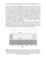
whole system to a halt. For example, Figure 10.2 shows an asynchronous
processor pipeline filling from the prefetch unit; here the system is halted
by a ‘HALT’ operation reaching the execution stage, at which point the
Chapter 10 Temporal Adaptation – Asynchronicity in Processor Design 233
preceding pipeline fills up and stalls while the subsequent stages stall be-
cause they are starved of input. When the halt is rescinded, the system will
resume where it left off and come to full speed almost instantaneously.
Thus, power management is extremely easy to implement and requires al-
most no software control.
Figure 10.2 Processor pipeline halting in execution stage.
In the Amulet processors, a halt instruction was retrofitted to the ARM
instruction set [12] by detecting an instruction which branches to itself.
This is a common way to implement an idle task on the ARM and causes
234 Steve Furber, Jim Garside
the processor to ‘spin’ until it is interrupted, burning power to no effect. In
Amulet2 and Amulet3, this instruction causes a local stall which rapidly
propagates throughout the system, reducing the dynamic power to zero. An
interrupt simply releases the stall condition, causing the processor to re-
sume and recognise the interrupt. This halt implementation is transparent –
as the effect of stopping is not distinguishable from the effect of repeating
an instruction which does not alter any data – except in the power con-
sumption.
Perhaps the most useful consequence of asynchronous systems only
processing data on demand is that this results in power savings throughout
the system. If a multiplier (for example) is not in use, it is not ‘clocked’
and therefore dissipates no dynamic power. This can be true of any subsys-
tem, but it is particularly important in infrequently used blocks.
10.4 Data-Dependent Timing
A well-engineered synchronous pipeline will usually be ‘balanced’ so that
the critical path in each stage is approximately the same length. This al-
lows the circuit to be clocked at its maximum frequency, without perform-
ance being wasted as a result of potentially faster stages being slowed to
the common clock rate. Good engineering is not easy, and considerable ef-
fort may need to be expended to achieve this.
The same principle holds in a self-timed system although the design con-
straints are different. A self-timed pipeline will find its own operating speed
in a similar fashion to traffic in a road system; a queue will form upstream of
a choke point and be sparser downstream. In a simulation, this makes it clear
where further design attention is required; this is usually – but not always –
the slowest stage. One reason why a particularly slow stage may not slow
the whole system is that it is on a ‘back road’ with very little traffic. There is
no requirement to process each operation in a fixed period, so the system
may adapt to its operating conditions. Here are some examples:
• In a memory system, some parts may go faster than others; cache
memories rely on this property and can be exploited even in synchro-
nous systems as a cache miss will stall for multiple clock cycles waiting
Of course, it is possible to gate clocks to mimic this effect, but clock
gating can easily introduce timing compatibility problems and is certainly
something which needs careful attention by the designer. Asynchronous
design delivers an optimal ‘clock gating’ system without any additional ef-
fort on the part of the designer.
Chapter 10 Temporal Adaptation – Asynchronicity in Processor Design 235
for an external response. This is the ‘natural’ behaviour of an asynchro-
nous memory where response is a single ‘cycle’ but the length of the
cycle is varied according to need. An advantage in the asynchronous
system is that it is easier to vary more parameters, and these can be al-
tered in more ‘subtle’ ways than simply in discrete multiples of clock
cycles.
• It is possible to exploit data dependency at a finer level. Additions are
slow because of carry propagation. To speed them up requires consider-
able effort, and hence hardware, and hence energy is typically expended
in fast carry logic of some form. This ensures that the critical path –
propagating a carry from the least to the most significant bit position –
is as short as possible. However, operations which require long carry
propagation distances are comparatively rare; the effort, hardware, and
power are expended on something which is rarely used. Given random
operands, the longest carry chain in an N-bit adder is O(N), but the av-
erage length is O(log
2
(N)); for a 32-bit adder the longest is about 6× the
average. If a variable-length cycle is possible, then a simple, energy-
efficient, ripple-carry adder can produce a correct result in a time com-
parable to a much larger (more expensive, power-consuming) adder.
• Not all operations take the same evaluation time: some operation
evaluation is data dependent. A simple example is a processor’s ALU
operation which typically may include options to MOVE, AND, ADD
or MULTIPLY operands. A MOVE is a fast operation and an AND, be-
ing a bitwise operation, is a similar speed. ADDs, however, are ham-
pered by the need to propagate carries across the datapath and therefore
are considerably slower. Multiplication, comprising repeated addition, is
of course slower still. A typical synchronous ALU will probably set its
critical path to the ADD operation and accept the inefficiency in the
MOVE. Multiplication may then require multiple clock cycles, with a
consequent pipeline stall, or be moved to a separate subsystem. An
asynchronous ALU can accommodate all of these operations in a single
cycle by varying the length of the cycle. This simplifies the higher-level
design – any stalls are implicit – and allows faster operations to com-
plete faster. It is sometimes said that self-timed systems can thus deliver
‘average case performance’; in practice, this is not true because it is
likely that the operation subsequent to a fast operation like MOVE will
not reach the unit immediately it is free, or the fast operation could be
stalled waiting for a previous operation to complete. Having a 50:50
mixture of 60mph cars and 20mph tractors does not mean the traffic
flows at 40mph! However, if the slow operations are quite rare – such as
multiplication in much code – then the traffic can flow at close to full
speed most of the time while the overall model remains simple.
236 Steve Furber, Jim Garside
Unfortunately, this is not the whole story because there is an overhead
in detecting the carry completion and, in any case, ‘real’ additions do
not use purely random operands [13]. Nevertheless, a much cheaper unit
can supply respectable performance by adapting its timing to the oper-
ands on each cycle. In particular, an incrementer, such as is used for the
programme counter, can be built very efficiently using this principle.
• At a higher level, it is possible to run different subsystems deliberately
at different rates. As a final example, the top level of the memory sys-
tem for Amulet3 is – as on many modern processors – split across sepa-
rate instruction and data buses to allow parallelism of access [14]. Here
these buses run to a unified local memory which is internally partitioned
into interleaved blocks. Provided two accesses do not ‘collide’, these
buses run independently at their own rates, and the bandwidth of the
more heavily loaded instruction bus – which is simpler because it can
only perform read operations – is somewhat higher than that of the
read/write, multi-master data bus. In the event that two accesses collide
in a single block, the later-arriving bus cycle is simply stretched to ac-
commodate the extra latency. Adaptability here gives the designer free-
dom: slowing the instruction bus down to match the two speeds would
result in lower performance, as would slowing the data bus to exactly
half the instruction bus speed.
The flexibility of asynchronous systems allows a considerable degree of
modularity in those systems’ development. Provided interfaces are com-
patible, it is possible to assemble systems and be confident that they will
not suffer from timing-closure problems – a fact which has been known for
some time [15]. It would be nice to say that such systems would always
work correctly! Unfortunately, this is not the case as, as in any complex
asynchronous system, it is possible to engineer in deadlocks; it is only tim-
ing incompatibilities which are eliminated. Where this is exploitable is in
altering or upgrading systems where a module – such as a multiplier – can
be replaced with a compatible unit with different properties (e.g. higher
speed or smaller area) with confidence that the system will not need exten-
sive resimulation and recharacterisation.
Perhaps the most important area to emerge from this is at a higher level,
i.e. in Systems-on-Chip (SoCs) using a GALS (Globally Asynchronous,
Locally Synchronous) approach [16]. Here conventional clocked IP blocks
are connected via an asynchronous fabric, effectively eliminating the
timing-closure problems at the chip level – at least from a functional view-
point. This can represent a considerable time-saving for the ASIC
designer.
Chapter 10 Temporal Adaptation – Asynchronicity in Processor Design 237
10.5 Architectural Variation in Asynchronous Systems
A pipelined architecture requires a succession of state-holding elements to
capture the output from one stage and hold it for the next. In a synchronous
architecture, these pipeline registers may be edge triggered (i.e. D-type
flip-flops) for simplicity of design; if this is too expensive then transparent
latches may be used, typically using a two-phase, non-overlapping clock
with alternating stages on opposite phases. The use of transparent latches
has largely been driven out in recent times by the need to accommodate the
limitations of synthesis and static timing analysis tools in high-productivity
design flows, so the more expensive and power-hungry edge-triggered reg-
isters have come to dominate current design practice.
10.5.1 Adapting the Latch Style
In some self-timed designs (e.g. dual-rail), the latches may be closely as-
sociated with the control circuits; however, a bundled-data datapath
closely resembles its synchronous counterpart. Because data is not trans-
ferred ‘simultaneously’ in all parts of the system, the simplicity (cheap-
ness) of transparent latches is usually the preferred option. Here the
‘downstream’ latch closes and then allows the ‘upstream’ latch to open at
any subsequent time. This operation can be seen in Figure 10.3 where
transparent latches are unshaded and closed latches shaded.
Here there is a design trade-off between speed and power. Figure 10.3
depicts an asynchronous pipeline in which the latches are ‘normally open’
– i.e. when the pipeline is empty all its latches are transparent; at the start
the system thus looks like a block of combinatorial logic. As data flows
through, the latches close behind it to hold it stable (or, put another way, to
delay subsequent changes) and then open again when the next stage has
captured its inputs. In the figure this is seen as a wave of activity as down-
stream latches close and, subsequently, the preceding latch opens again.
When the pipeline is empty (clear road ahead!), this model allows data to
flow at a higher speed than is possible in a synchronous pipeline because
the pipeline latency is the sum of the critical paths in the stages rather than
the multiple of the worst-case critical path and the pipeline depth.
The price of this approach is a potential increase in power consumption.
The data ‘wave front’ will tend to skew as it flows through the logic,
which can cause the input of a gate to change more times than it would if
the wave front were re-aligned at every stage. This introduces glitches into
the data which result in wasted energy due to the spurious transitions
which can propagate considerable distances.
238 Steve Furber, Jim Garside
Figure 10.3 Pipeline with ‘normally open’ latches. Open latches are unshaded;
closed latches are shaded.
To prevent glitch propagation, the pipeline can adopt a ‘normally closed’
architecture (Figure 10.4). In this approach, the latches in an empty pipe-
line remain closed until the data signalls its arrival, at which point they
open briefly to ‘snap up’ the inputs. The wave of activity is therefore visi-
ble as a succession of briefly transparent latches (unshaded in the figure).
Chapter 10 Temporal Adaptation – Asynchronicity in Processor Design 239
Figure 10.4 Pipeline with ‘normally closed’ latches. Open latches are unshaded;
closed latches are shaded.
Their outputs therefore change nearly simultaneously, re-aligning the data
wave front and reducing the chance of glitching in the subsequent stage.
The disadvantage of this approach is that data propagation is slowed wait-
ing for latches, which are not retaining anything useful, to open.
These styles of latch control can be mixed freely. The designer has the
option of increased speed or reduced power. If the pipeline is filled to its
maximum capacity, the decision is immaterial because the two behaviours
can be shown to converge. However, in other circumstances a choice has
to be made. This allows some adaptivity to the application at design time,
but the principle can be extended so that this choice can be made dynami-
cally according to the system’s loading.
240 Steve Furber, Jim Garside
Figure 10.5 Configurable asynchronous latch controller.
The two latch controllers can be very similar in design – so much so that
a single additional input (two or four additional transistors, depending on
starting point) can be used to convert one to the other (Figure 10.5). Fur-
thermore, provided the change is made at a ‘safe’ time in the cycle, this in-
put can be switched dynamically. Thus, an asynchronous pipeline can be
equipped with both ‘sport’ and ‘economy’ modes of operation using
‘Turbo latches’ [17].
The effectiveness of using normally closed latches for energy conserva-
tion has been investigated in a bundled-data environment; the result de-
pends strongly on both the pipeline occupancy and, as might be expected,
the variation in the values of the bits flowing down the datapath.
The least favourable case is when the pipeline is fully occupied, when
even a normally open latch will typically not open until about the time that
new data is arriving; in this case, there is no energy wastage due to the
propagation of earlier values. In the ‘best’ case, with uncorrelated input
data and low pipeline occupancy, an energy saving of ~20% can be
achieved at a price of ~10% performance, or vice versa.
10.5.2 Controlling the Pipeline Occupancy
In the foregoing, it has tacitly been assumed that processing is handled in
pipelines. Some applications, particularly those processing streaming data,
naturally map onto deep pipelines. Others, such as processors, are more
problematic because a branch instruction may force a pipeline flush and
any speculatively fetched instructions will then be discarded, wasting en-
ergy. However, it is generally not possible to achieve high performance
without employing pipelining.
Chapter 10 Temporal Adaptation – Asynchronicity in Processor Design 241
Figure 10.6 Occupancy throttling using token return mechanism.
In a synchronous processor, the speculation depth is effectively set by
the microarchitecture. It is possible to leave stages ‘empty’, but there is no
great benefit in doing so as the registers are still clocked. In an asynchro-
nous processor, latches with nothing to do are not ‘clocked’, so it is sensi-
bly possible to throttle the input to leave gaps between instruction packets
and thus reduce speculation, albeit at a significant performance cost. This
can be done, for example, when it is known that a low processing load is
required or, alternatively, if it is known that the available energy supply is
limited. Various mechanisms are possible: a simple throttle can be imple-
mented by requiring instruction packets to carry a ‘token’ through the
pipeline, collecting it at fetch time and recycling it when they are retired
(Figure 10.6). For full-speed operation, there must be at least as many to-
kens as there are pipeline stages so that no instruction has to wait for a to-
ken and flow is limited purely by the speed of the processing circuits.
However, to limit flow, some of the tokens (in the return pipeline) can be
removed, thus imposing an upper limit on pipeline occupancy. This limit
can be controlled dynamically, reducing speculation and thereby cutting
power as the environment demands.
An added bonus to this scheme is that if speculation is sufficiently lim-
ited, other power-hungry circuits such as branch prediction can be disabled
without further performance penalty.
10.5.3 Reconfiguring the Microarchitecture
Turbo latches can alter the behaviour of an asynchronous pipeline, but they
are still latches and still divide the pipeline up into stages which are fixed
in the architecture. However, in an asynchronous system adaptability can
be extended further; even the stage sizes can be altered dynamically!
242 Steve Furber, Jim Garside
A ‘normally open’ asynchronous stage works in this manner:
1. Wait for the stage to be ready and the arrival of data at the input latch;
2. Close the input latch;
3. Process the data;
4. Close the output latch;
5. Signal acknowledgement;
6. Open the input latch.
Such latching stages operate in sequence, with the whole task being parti-
tioned in an arbitrary manner.
If another latch was present halfway through data processing (step 3,
above), this would subdivide the stage and produce the acknowledgement
earlier than otherwise. The second half of the processing could then con-
tinue in parallel with the recovery of the earlier part of the stage, which
would then be able to accept new data sooner. The intermediate latch
would reopen again when the downstream acknowledgement (step 5,
above) reached it, ready to accept the next packet. This process has subdi-
vided what was one pipeline stage into two, potentially providing a near
doubling in throughput at the cost of some extra energy in opening and
closing the intermediate latch.
In an asynchronous pipeline, interactions are always local and it is pos-
sible to alter the pipeline depth during operation knowing that the rest of
the system will accommodate the change. It is possible to tag each data
packet with information to control the latch behaviour. When a packet
reaches a latch, it is forced into local synchronisation with that stage. In-
stead of closing and acknowledging the packet the controller can simply
pass it through by keeping the latch transparent and forwarding the control
signal. No acknowledgement is generated; this will be passed back when it
appears from the subsequent stage. In this manner, a pipeline latch can be
removed from the system, altering the microarchitecture in a fundamental
way. In Figure 10.7, packet ‘B’ does not close – and therefore ‘eliminates’
– the central latch; this and subsequent operations are slower but save on
switching the high-capacitance latch enable.
Of course, this change is reversible; a latch which has been deactivated
can spot a reactivation command flowing through and close, reinstating the
‘missing’ stage in the pipeline. In Figure 10.8, packet ‘D’ restores the cen-
tral latch allowing the next packet to begin processing despite the fact that
(in this case) packet ‘C’ appears to have stalled.
Why might this be useful? The technique has been analysed in a proces-
sor model using a range of benchmarks [18–20]. As might be expected,
collapsing latches and combining pipeline stages – in what was, initially, a
reasonably balanced pipeline – reduces overall throughput by, typically,
Chapter 10 Temporal Adaptation – Asynchronicity in Processor Design 243
50–100%. Energy savings are more variable: streaming data applications
that contain few branches show no great benefit; more ‘typical’ micro-
processor applications with more branches exhibit ~10% energy savings
and, as might be expected, the performance penalty is at the lower end of
the range. If this technique is to prove useful, it is certainly one which
needs to be used carefully and applied dynamically, possibly under soft-
ware control; however, it can provide benefits and is another tool available
to the designer.
Figure 10.7 Pipeline collapsing and losing latch stage.
Figure 10.8 Pipeline expanding and reinstating latch stage.
244 Steve Furber, Jim Garside
10.6 Benefits of Asynchronous Design
Asynchronous operation brings diverse benefits to microprocessors, but
these are in general hard to quantify. Unequivocal comparisons with
clocked processors are few and far between. Part of the difficulty lies in
the fact that there are many ways to build microprocessors without clocks,
each offering its own trade-offs in terms of performance, power efficiency,
adaptability, and so on. Exploration of asynchronous territory has been far
less extensive than that of the clocked domain, so we can at this stage only
point to specific exemplars to see how asynchronous design can work out
in practice.
The Amulet processor series demonstrated the feasibility, technical
merit, and commercial viability of asynchronous processors. These full-
custom designs showed that asynchronous processor cores can be competi-
tive with clocked processors in terms of area and performance, with dra-
matically reduced electromagnetic emissions. They also demonstrated
modest power savings under heavy processing loads, with greatly simpli-
fied power management and greater power savings under variable event-
driven workloads.
The Philips asynchronous 80C51 [7] has enjoyed considerable commer-
cial success, demonstrating good power efficiency and very low electro-
magnetic emissions. It is a synthesised processor, showing that asynchro-
nous synthesis is a viable route to an effective microprocessor, at least at
lower performance levels.
The ARM996HS [8], developed in collaboration between ARM Ltd and
Handshake Solutions, is a synthesised asynchronous ARM9 core available
as a licensable IP core with better power efficiency (albeit at lower per-
formance) than the clocked ARM9 cores. It demonstrated low current
peaks and very low electromagnetic emissions and is robust against cur-
rent, voltage, and temperature variations due to the intrinsic ability of the
asynchronous technology to adapt to changing environmental conditions.
All of the above designs employ conventional instruction set architec-
tures and have implemented these in an asynchronous framework while
maintaining a high degree of compatibility with their clocked predeces-
sors. This compatibility makes comparison relatively straightforward, but
may constrain the asynchronous design in ways that limit its potential.
More radical asynchronous designs have been conceived that owe less to
the heritage of clocked processors, such as the Sun FLEET architecture
[21], but there is still a long way to go before the comparative merits of
these can be assessed quantitatively.
Chapter 10 Temporal Adaptation – Asynchronicity in Processor Design 245
10.7 Conclusion
Although almost all current microprocessor designs are based on the use of
a central clock, this is not the only viable approach. Asynchronous design,
which dispenses with global timing control in favour of local synchronisa-
tion as and when required, introduces several potential degrees of adapta-
tion that are not readily available to the clocked system. Asynchronous cir-
cuits intrinsically adapt to variations in supply voltage (making dynamic
voltage scaling very straightforward), temperature, process variability,
crosstalk, and so on. They can adapt to varying processing requirements, in
particular enabling highly efficient event-driven, real-time systems. They
can adapt to varying data workloads, allowing hardware resources to be
optimised for typical rather than very rare operand values, and they can
adapt very flexibly (and continuously, rather than in discrete steps) to vari-
able memory response times. In addition, asynchronous processor mi-
croarchitectures can adapt to operating conditions by varying their funda-
mental pipeline behaviour and effective pipeline depth.
The flexibility and adaptability of asynchronous microprocessors make
them highly suited to a future that holds the promise of increasing device
variability. There remain issues relating to design tool support for asyn-
chronous design, and a limited resource of engineers skilled in the art, but
the option of global synchronisation faces increasing difficulties, at least
some of which can be ameliorated through the use of asynchronous design
techniques. We live in interesting times for the asynchronous microproces-
sor; only time will tell how the balance of forces will ultimately resolve.
References
[1] A.J. Martin, S.M. Burns, T.K. Lee, D. Borkovic and P.J. Hazewindus, “The
Design of an Asynchronous Microprocessor”, ARVLSI: Decennial Caltech
Conference on VLSI, ed. C.L. Seitz, MIT Press, 1989, pp. 351–373.
[2] S.B. Furber, P. Day, J.D. Garside, N.C. Paver and J.V. Woods, “AMULET1:
A Micropipelined ARM”, Proceedings of CompCon'94, IEEE Computer So-
ciety Press, San Francisco, March 1994, pp.476–485.
[3] A. Takamura, M. Kuwako, M. Imai, T. Fujii, M. Ozawa, I. Fukasaku, Y.
Ueno and T. Nanya, “TITAC-2: A 32-Bit Asynchronous Microprocessor
Based on Scalable-Delay-Insensitive Model”, Proceedings of ICCD'97, Oc-
tober 1997, pp. 288–294.
[4] M. Renaudin, P. Vivet and F. Robin, “ASPRO-216: A Standard-Cell Q.D.I.
16-Bit RISC Asynchronous Microprocessor”, Proceedings of Async'98,
IEEE Computer Society, 1998, pp. 22–31. ISBN:0-8186-8392-9.
246 Steve Furber, Jim Garside
[5] S.B. Furber, J.D. Garside and D.A. Gilbert, “AMULET3: A High-
Performance Self-Timed ARM Microprocessor”, Proceedings of ICCD'98,
Austin, TX, 5–7 October 1998, pp. 247–252. ISBN 0-8186-9099-2.
[6] S.B. Furber, A. Efthymiou, J.D. Garside, M.J.G. Lewis, D.W. Lloyd and S.
Temple, “Power Management in the AMULET Microprocessors”, IEEE De-
sign and Test of Computers, ed. E. Macii, March–April 2001, Vol. 18, No. 2,
pp. 42–52. ISSN: 0740-7475.
[8] A. Bink and R. York, “ARM996HS: The First Licensable, Clockless 32-Bit
Processor Core”, IEEE Micro, March 2007, Vol. 27, No. 2, pp. 58–68. ISSN:
0272-1732.
[9] I. Sutherland, “Micropipelines”, Communications of the ACM, June 1989,
Vol. 32, No. 6, pp.720–738. ISSN: 0001-0782.
[10] J. Sparsø and S. Furber (eds.), “Principles of Asynchronous Circuit Design –
A Systems Perspective”, Kluwer Academic Publishers, 2002. ISBN-10:
0792376137 ISBN-13: 978-0792376132.
[11] S.B. Furber, D.A. Edwards and J.D. Garside, “AMULET3: A 100 MIPS
Asynchronous Embedded Processor”, Proceedings of ICCD'00, 17–20 Sep-
tember 2000.
[12] D. Seal (ed.), “ARM Architecture Reference Manual (Second Edition)”, Ad-
dison-Wesley, 2000. ISBN-10: 0201737191 ISBN-13: 978-0201737196.
[13] J.D. Garside, “A CMOS VLSI Implementation of an Asynchronous
ALU”,“Asynchronous Design Methodologies”, eds. S.B. Furber and M. Ed-
wards, Elsevier 1993, IFIP Trans. A-28, pp. 181–207.
[14] D. Hormdee and J.D. Garside, “AMULET3i Cache Architecture”, Proceed-
ings of Async’01, IEEE Computer Society Press, March 2001, pp. 152–161.
ISSN 1522-8681 ISBN 0-7695-1034-4.
[15] W.A. Clark, “Macromodular Computer Systems”, Proceedings of the Spring
Joint Conference, AFIPS, April 1967.
[16] D.M. Chapiro, “Globally-Asynchronous Locally-Synchronous Systems”,
Ph.D. thesis, Stanford University, USA, October 1984.
[17] M. Lewis, J.D. Garside and L.E.M. Brackenbury, “Reconfigurable Latch
Controllers for Low Power Asynchronous Circuits”, Proceedings of
Async'99, IEEE Computer Society Press, April 1999, pp. 27–35.
[18] A. Efthymiou, “Asynchronous Techniques for Power-Adaptive Processing”,
Ph.D. thesis, Department of Computer Science, University of Manchester,
UK, 2002.
[19] A. Efthymiou and J.D. Garside, “Adaptive Pipeline Depth Control for Proc-
essor Power-Management”, Proceedings of ICCD'02, Freiburg, September
2002, pp. 454–457. ISBN 0-7695 1700-5 ISSN 1063-6404.
[7] H. van Gageldonk, K. van Berkel, A. Peeters, D. Baumann, D. Gloor and
G. Stegmann, “An Asynchronous Low-Power 80C51 Microcontroller”, Pro-
ceedings of Async'98, IEEE Computer Society, 1998, pp. 96–107. ISBN:0-
8186-8392-9.
Chapter 10 Temporal Adaptation – Asynchronicity in Processor Design 247
[21] W.S. Coates, J.K. Lexau, I.W. Jones, S.M. Fairbanks and I.E. Sutherland,
“FLEETzero: An Asynchronous Switching Experiment”, Proceedings of
Async'01, IEEE Computer Society, 2001, pp. 173–182. ISBN:0-7695-1034-5.
[20] A. Efthymiou and J.D. Garside, “Adaptive Pipeline Structures for Specula-
tion Control”, Proceedings of Async'03, Vancouver, May 2003, pp. 46–55.
ISBN 0-7695-1898-2 ISSN 1522-8681.
Chapter 11 Dynamic and Adaptive Techniques
John J. Wuu
Advanced Micro Devices, Inc.
11.1 Introduction
The International Technology Roadmap for Semiconductors (ITRS)
predicted in 2001 that by 2013, over 90% of SOC die area will be occupied
by memory [7]. Such level of integration poses many challenges, such as
power, reliability, and yield. In addition, as transistor dimensions continue
to shrink, transistor threshold voltage (V
T
) variation, which is inversely
proportional to the square root of the transistor area, continues to increase.
This V
T
variation, along with other factors contributing to overall
variation, is creating difficulties in designing stable SRAM cells that meet
product density and voltage requirements.
This chapter examines various dynamic and adaptive techniques for
mitigating some of these common challenges in SRAM design. The
chapter first introduces innovations at the bitslice level, which includes
SRAM cells and immediate peripheral circuitry. These innovations seek to
improve bitcell stability and increase the read and write margins, while
reducing power. Next, the power reduction techniques at the array level,
which generally involve cache sleeping and methods for regulating the
sleep voltage, as well as schemes for taking the cache into and out of sleep
are discussed. Finally, the chapter examines the yield and reliability,
which are issues that engineers and designers cannot overlook, especially
as caches continue to increase in size. To improve reliability, one must
account for test escapes, latent defects, and soft errors; thus the chapter
concludes with a discussion of error correction and dynamic cache line
disable or reconfiguration options.
in SRAM Design
A. Wang, S. Naffziger (eds.), Adaptive Techniques for Dynamic Processor Optimization,
DOI: 10.1007/978-0-387-76472-6_11, © Springer Science+Business Media, LLC 2008
250 John J. Wuu
11.2 Read and Write Margins
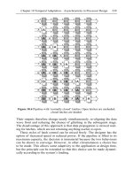
Figure 11.1 illustrates the basic 6-Transistor (6T) SRAM cell, with back-
to-back inverters holding the storage node values and access transistors
allowing access to the storage nodes. In Figure 11.1, the transistors in the
inverter are labeled as M
P
and M
N
, while the access transistor is labeled as
M
A
. M
P
, M
N
, and M
A
are used when referring to transistors in the SRAM
cell.
M
A
M
N
M
P
M
P
M
N
M
A
Figure 11.1 Basic SRAM cell.
As basic requirements, a SRAM cell must maintain its state during a
read access and be capable of changing state during a write operation. In
other words, a cell must have positive read and write margins.
While there are many different methods to quantify a SRAM cell’s read
margin, graphically deriving the Static Noise Margin (SNM) through the
butterfly curve, as introduced in [17] and described in Chapter 6, remains a
common approach. In addition to its widespread use, the butterfly curve
can conveniently offer intuitive insight into a cell’s sensitivity to various
parameters. The butterfly curve is used to facilitate the following
discussion.
Chapter 11 Dynamic and Adaptive Techniques in SRAM Design 251
V
0
(a) (b)
Figure 11.2 Butterfly curves.
Figure 11.2a illustrates the butterfly curve of a typical SRAM cell. As
introduced in Chapter 6, SNM is defined by the largest square that can fit
between the two curves. Studying the butterfly curve indicates that to
enlarge the size of the SNM square, designers must lower the value of V
0
.
Since V
0
is determined by the inverse of M
N
/M
A
, the M
N
/M
A
ratio must be
high. The large arrow in Figure 11.2b illustrates the effect of increasing
the M
N
/M
A
ratio. However, increasing M
N
has the side effect of
decreasing the M
P
/M
N
ratio (highlighted by the small arrow), which would
slightly decrease SNM. Following this logic concludes that increasing M
P
to achieve higher M
P
/M
N
ratio could also improve a cell’s SNM.
On the other hand, to achieve good write margin, a “0” on the bitline
must be able to overcome M
P
holding the storage node at “1” through M
A
.
Therefore, decreasing M
A
and increasing M
P
to improve SNM would
negatively impact the write margin. In recent process nodes, with voltage
scaling and increased device variation, it is becoming difficult to satisfy
both read and write margins.
The following sections will survey the range of techniques that seek to
dynamically or adaptively improve SRAM cells’ read and write margins.
11.2.1 Voltage Optimization Techniques
Because a SRAM cell’s stability is highly dependent on the supply
voltage, voltage manipulation can impact a cell’s read and write margins.
252 John J. Wuu
Voltage manipulation techniques can be roughly broken down into row
and column categories, based on the direction of the voltage manipulated
cells.
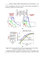
11.2.1.1 Column Voltage Optimization
To achieve high read and write margins, a SRAM cell must be stable
during a read operation and unstable during a write operation. One way to
accomplish this is by providing the SRAM cell with a high VDD during
read operations and a low VDD during write operations. One example
[22] is the implementation of a dual power supply scheme. As shown in
Figure 11.3, multiplexers allow either the high or the low supply to power
the cells on a column-by-column basis. During standby operation, the low
supply is provided to all the cells to decrease leakage power. Cell stability
can be maintained with this lower voltage because the cells are not being
accessed; thus, the bitlines do not disturb the storage nodes through M
A
.
When the cells are accessed in a read operation, the row of cells with the
active wordline (WL) experiences a read-disturb, which reduces the
stability of the SRAM cells; therefore, the high supply is switched to all
the columns to improve the accessed cells’ stability. During a write
operation, the columns that are being written to remain on the low supply,
allowing easy overwriting of the cells. Assuming a column-multiplexed
implementation, the columns not being written to are provided with the
higher supply, just like in a read operation, to prevent data corruption from
the disturb.
VCC_hi
VCC_lo
W
WL
SRAMVCC
WL
MUX (8:1)
RRR
cellcellcellcell cell
cell cell cell cell cell
Figure 11.3 Dual supply column-based voltage optimization [22]. (© 2006 IEEE)