Adaptive Techniques for Dynamic Processor Optimization Theory and Practice Episode 2 Part 6 ppt
Bạn đang xem bản rút gọn của tài liệu. Xem và tải ngay bản đầy đủ của tài liệu tại đây (472.38 KB, 20 trang )
Chapter 11 Dynamic and Adaptive Techniques in SRAM Design 253
2nd Metal
#WE
WE[n+1]
WE[n]
4th Metal
n_arvdd
n+1_arvdd
downvdd
n_Bit n_#Bit n+1_Bit
n+1_#Bit
Capacitive Write
Assist Circuit
WL
WL
P-Tr[n]
N-Tr[n]
P-Tr[n+1]
N-Tr[n+1]
Nd-Tr
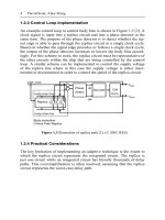
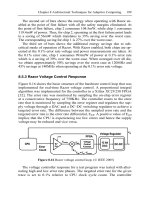
Figure 11.4 Charge sharing for supply reduction [14]. (© 2007 IEEE)
Since extra supplies are not always available in product design, another
example [14] uses charge sharing to lower the supply to the columns being
written to. As shown in Figure 11.4, “downvdd” is precharged to VSS.
For a write operation, supplies to the selected columns are disconnected
from VDD, and shorted to “downvdd”. The charge sharing lowers the
supply’s voltage to a level determined by the ratio of the capacitances,
allowing writes to occur easily.
254 John J. Wuu
Memory cell
Memory cell Memory cell
Memory cell
Vssm
Vdd
Vddm[n]
Vddm[n+1]
WCLM[n] WCLM[n+1]
MSW[n]
MSW[n+1]
Figure 11.5 Write column supply switch off [21]. (© IEEE 2006)
Yet another example [21] uses a power-line-floating write technique to
assist write operations. Instead of switching in a separate supply or charge
sharing the supply, as in previous examples, the supply to the write columns is
simply switched off, floating the column supply lines at VDD (Figure 11.5).
As the cells are written to, the floating supply line (Vddm) discharges
through the “0” bitline, as shown in Figure 11.6a. The decreased supply
voltage allows easy writing to the cells. As soon as the cell flips to its
intended state, the floating supply line’s discharge path is cut off, preventing
the floating supply line from fully discharging (Figure 11.6b).
Iwrite
“L”
“L”
“H”
“H”
Vddm
Vddm
“H”“L”
“L” “H”
(a) (b)
Figure 11.6 Power-line-floating write [21]. (© IEEE 2006)
Chapter 11 Dynamic and Adaptive Techniques in SRAM Design 255
In all column voltage manipulation schemes, nonselected cells must
retain state with the lowered supply.
11.2.1.2 Row Voltage Optimization
Similar to the previous section, designers can apply voltage manipulation
in the row direction as well. However, unlike column-based voltage
optimization, row-based voltage optimization generally cannot
simultaneously optimize for both read and write margins in the same
operation, as needed in a column-multiplexed design. Therefore, row-
based voltage manipulation tends to be more suitable for non-column-
multiplexed designs where all the columns are written to in a write
operation.
The most obvious method to apply row-based voltage optimization is to
raise the supply for the row of accessed cells in a read operation, or to
lower the supply for the row of cells being written to. In addition, the
following are some other examples of row-based voltage optimization.
“L”
“L”
“H”“H”
“H”
“H”“H”
“H”
Word Line
Ld1
Dr1
“L”
Tr1
Node A
MS1
MD1
MR1
Vss
PLVC1
Vdd
Ic2
Ic1
sw1
Vss_mem
cellb x3
Ic1
Ic2
cella
Node B
Figure 11.7 Raised source line write [20]. (© IEEE 2004)
In [20], the SRAM cells’ source line (SL) (i.e., source terminals of M
N
s
in Figure 11.1) is disconnected from VSS during write operations. The SL
is allowed to float until it is clamped by an NFET diode (Figure 11.7). The
raised SL (Vss_mem in Figure 11.7) decreases the drive of the PFETs,
which allows easy overwriting of the cell. (In this specific example, the
floating SL is shared among all the cells in the array, not just the cells in a
row. However, designers can apply the same technique on a row-by-row
256 John J. Wuu
basis at the cost of area overhead.) A variation of this technique would
disconnect the SL during both write and standby operations to achieve
power savings, and connect the SL to VSS only during read operations
when the extra stability margin is needed. The drawback to this variation
is the additional delay needed to restore SL to VSS before a read operation
can begin.
A similar example [13] also floats SL during write operations. In
addition, the SL is driven to a negative voltage during read operations.
This allows for faster bitline development, as well as more stable cells
during read operations.
VGND
BLC BLTPL2PL1
PL1
PL2
PL3
PL0
WL0
WL1
WL2
SRAM cell Subarray
VDD
VDD
VDD
VDD VDD
VDD
VDD
VDD
WL1 WL1
Figure 11.8 Supply line coupling [3]. (© IEEE 2004)
If a separate supply is not available, another way to boost the internal
supply of SRAM cells during a read access to achieve higher stability is
through coupling. In [3], wordline wires are routed next to the row’s
supply lines. As seen in Figure 11.8, as the wordline rises, it disconnects
the supply lines from VDD, and couples the voltages of the supply lines
higher than VDD. Assuming insignificant current is sourced from the
supply line during a read access, the bootstrapped supply increases the
drive on M
N
s and improves the cell’s stability. However, for cell designs
with low M
N
/M
A
ratios, the “0” storage node may rise higher than M
N
’s
threshold voltage, causing the floating supply lines to discharge.
Chapter 11 Dynamic and Adaptive Techniques in SRAM Design 257
WL-driver
n_arvdd
n_Bit n_#Bit
Replica
Access Tr
Read Assist
Circuit
WL
WL
WL
P
WL
N
WL
P
WL
N
WL
P
WL
N
WL
Figure 11.9 Wordline driver using RATs [14]. (© IEEE 2007)
In [14], instead of increasing the SRAM cell’s supply to improve
stability, the WL voltage is reduced slightly. Reduced wordline voltage
degrades the drive of M
A
, which essentially improves the M
N
/M
A
ratio.
This implementation makes additional efforts to account for global
threshold voltage variations. Figure 11.9 illustrates the scheme, using
“replica access transistors” (RATs) that have almost the same physical
topology as M
A
to lower the WL voltage. In general, lower V
TN
causes
SRAM cells to be less stable. Therefore, the RATs lower WL more when
V
TN
is low, and less when V
TN
is high, to achieve balance between read
margin and read speed.
11.2.2 Timing Control
Aside from voltage manipulation, designers can also improve cell stability
by decreasing the amount of time the cell is under stress during a read
operation. For example, in a design that uses differential sensing, a small
bitline voltage drop could be sufficient for sensing the bitcell value.
Leaving on the wordline longer than necessary would allow the bitlines to
continue to disturb the “0” storage node, leading marginal SRAM cells to
flip their values.
In typical designs, the wordline shutoff is triggered on phase or cycle
boundaries. If the optimal wordline shutoff time does not align with phase
or cycle boundaries, or if the designer prefers to have the wordline high
time independent of the frequency, then the designer could employ a
258 John J. Wuu
pulsed wordline scheme, such as the one used in [11]. The challenge is to
design the appropriate pulse width that is just long enough for reads to
complete successfully across different process corners and operating
conditions.
MC MC MC MC
MC MC MC MC
MC MC MC MC
MC MC MC MC
RC
RC
RC
RC
WL
WDR
WDR
WDR
WDR
WOFF
REN
RW
WEN
MPC
RB
MWR
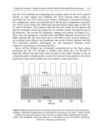
Figure 11.10 Read and write replica circuits [21]. (© IEEE 2006)
In [15], a read replica path, which uses 12 dummy SRAM cells, was
used for generating the shutoff edge for wordlines. The dummy SRAM
cells, which resemble real SRAM cells but have internal values hardwired,
help the replica path to track the variation in normal read paths. In
addition to the read replica circuits [21], a write replica circuit was also
added. In general, read operations take more time to complete than write
operations. Therefore, it is advantageous to shut off the wordline during a
write operation as soon as the write is completed successfully, which will
prevent unselected columns in a column-multiplexed design from conti-
nuing to discharge the bitlines, resulting in wasted power. Figure 11.10 is
an example illustrating the read and write replica paths together. The
replica bitline (RB) is precharged to VDD through MPC before read or
write operations begin. For a read operation, REN activates to “0”,
causing the read-replica wordline (RW) to turn on the read dummy cells’
(RC) wordline. The RC’s discharge RB, which turns off the wordlines
through the WOFF signal. In a write operation, RB is discharged through
MWR, which also triggers WOFF. In general, higher V
TN
requires the
write time to be longer. Therefore, dies with higher V
TN
would have a
slower discharge through MWR, providing the write operation more time
to complete.
Chapter 11 Dynamic and Adaptive Techniques in SRAM Design 259
The above illustration is just one example of designs using replica
circuits. The danger of replica circuits, of course, is no replica can
perfectly track real paths through all process and operating corners. For
example, the write replica circuit above does not track PFET variations,
which also impact write margin. However, tracking some variation can
usually yield more optimal designs than no tracking at all.
11.3 Array Power Reduction
With power-per-performance becoming an important parameter, engineers
pay increasing attention to reducing the power of embedded SRAM arrays,
which often occupy a large percentage of the total die area. Since activity
factor is generally low for large caches, leakage power represents a
significant, if not the dominant, portion of the overall cache power.
Devices in a SRAM cell typically have channel lengths much greater than
the process minimum for variation control; thus, subthreshold leakage has
traditionally been limited. However, subthreshold leakage has worsened
with recent technology nodes and more importantly, gate leakage (and in
some cases, junction leakage) is getting significantly worse with oxide
scaling. As a result, SRAM leakage power now requires careful attention.
Because leakage power has a strong dependence on voltage, many have
experimented with or implemented with “sleeping” the cache’s supply.
11.3.1 Sleep Types
In general, cache “sleep” involves providing inactive SRAM cells, which
do not experience read-disturb, with a lowered supply to achieve power
savings. The lowered supply must be high enough to allow the inactive
cells to maintain their data. Then, before the cells are accessed, they are
“woken up” by providing a higher supply that can fulfill both read-disturb
and access speed requirements.
The most straightforward implementation of cache sleep involves
providing the cache with two separate, external supplies. However, a
second supply is an expensive solution, so realistic implementations often
choose to generate and regulate the second supply locally. In general,
these implementations fall into two categories – active and passive.
“Active sleep” schemes try to actively maintain the reduced voltage at a
certain level, while “passive sleep” schemes rely on voltage division or
threshold voltage to determine the reduced voltage.
260 John J. Wuu
11.3.1.1 Active Sleep
Khellah et al. [10] used an op-amp to help control the reduced supply;
Figure 11.11 illustrates its general concept. When the arrays are active,
“wake” causes SramVSS to be connected to VSS through the strong
NFET. During idle mode, the strong NFET is turned off, allowing
SramVSS to float. SramVSS will rise due to array leakage, but the op-amp
will prevent SramVSS from rising above VREF. Of course, VDD – VREF
must be greater than the SRAM cells’ standby VccMin, which is the
minimum voltage at which cells are stable, to maintain cell data. In this
implementation, VREF is externally supplied for ease of controllability.
Also, an “early wake” signal is provide ahead of “wake”, to reduce the
ground-bounce noise due to sudden discharge of SramVSS.
Jumel et al. [8] used a similar concept as the previous example, but took
it a step further. As shown in Figure 11.12, an on-chip bandgap reference
generates a reference voltage that is stable across PVT. In addition, the
voltage regulator is designed to track VDD, so a higher VDD would also
allow SramVSS to rise, maintaining VDD – SramVSS close to VccMin.
Finally, the output of this regulator is trimmed on a die-by-die basis at
wafer probe to account for process variations.
Figure 11.11 Active sleep control [10]. (© IEEE 2006)
Chapter 11 Dynamic and Adaptive Techniques in SRAM Design 261
VREF
Startup
Circuit
Reference
Bandgap
-
+
Error
Amplifier
Analog
Supply
Logic
Supply
GND
SramVSS
(to SRAM)
Figure 11.12 Active sleep control with bandgap reference and VDD tracking [8].
(© IEEE 2006) Courtesy of Philippe Royannez: Texas Instruments, Inc.
11.3.1.2 Passive Sleep
One straightforward way to generate a reduced supply is to use a diode,
such as in [1] and illustrated in Figure 11.13. When SramVSS rises to the
diode’s threshold voltage, the diode would clamp SramVSS. The
downside to this scheme is its inflexibility, as the clamping voltage is
determined primarily by just the threshold voltage, and cannot be
optimized for different supply voltages.
wake
SramVSS
SRAM array
Figure 11.13 Diode clamping sleep voltage.
262 John J. Wuu
SramVSS
Figure 11.14 Bias generator with replica transistors [18]. (© IEEE 2006)
The example shown in Figure 11.14 aims to remove the SRAM supply’s
dependency on VDD [18]. Rather than setting the array supply to VDD –
V
T
, which can vary depending on VDD, the array supply depends only on
transistor threshold voltages, as specified in Equation (11.1).
Array supply = 2 * Max(V
T
(M
N
), V
T
(M
P
)) (11.1)
In this implementation, the array supply voltage specified in Equation
(11.1) is assumed to be sufficient for satisfying VccMin requirements. To
adapt to different PVT conditions, the bias generator is built using replica
transistors. The two replica load PFETs drop A1’s voltage to
A1 = VDD – 2 * V
T
(M
P
) (11.2)
Similarly, the two replica driver NFETs drop A2’s voltage to
A2 = VDD – 2 * V
T
(M
N
) (11.3)
Finally, the matching P1 and P1’ FETs clamp SramVSS at A1, while the
matching P2 and P2’ FETs clamp SramVSS at A2. The resulting
SramVSS is the lower of A1 and A2, producing Equation (11.1).
Chapter 11 Dynamic and Adaptive Techniques in SRAM Design 263
sleepn
SramVSS
shutoff
BL
BL#
Sleep biasing control
MND
MPB
Figure 11.15 Passive sleep with parallel pull-down transistors [4]. (© IEEE 2007)
In yet another example of passive cache sleep [4], a group of NFETs of
different sizes were built in parallel between SramVSS and VSS, as shown
in Figure 11.15. In this implementation, VSS is gated by a shut-off FET to
support cache power-down. During silicon characterization, the optimal
combination of these NFETs is determined to maximize leakage power
savings while maintaining cell stability. To provide better immunity from
temperature variation, MND and MPB were added to the bias generator.
In high temperature regions, the increased cell leakage would cause
SramVSS to rise, reducing the supply to the memory cells and
compromising stability. In such regions, the reduced V
T
s for MND and
MPS due to the high temperature would strengthen the pull-down, and
reduce the amount that SramVSS rises.
11.3.2 P Versus N Sleep
All the examples shown above use N-sleep, which provides the SRAM
cells with true VDD and regulates SramVSS. Before accessing the SRAM
cells, NFETs are used to restore SramVSS to VSS. Of course, designers
can also implement the complementary P-sleep. In P-sleep designs, SRAM
cells are provided with true VSS and a regulated SramVDD. Before
accessing the P-sleep SRAM cells, PFETs are used to restore SramVDD
to VDD.
264 John J. Wuu
“0”
“1”
“1”
“0” “1”
Figure 11.16 Junction leakage paths in SRAM cell.
At first glance, N-sleep seems the obvious favorite because the superior
current driving capability of NFETs allows for smaller wake-up
transistors, thus producing more efficient designs. However, designers
must consider additional factors to make the appropriate choice. For
example, the VSS net in a SRAM array often has more capacitance than
the VDD net, so the larger SramVSS capacitance that must be discharged
may negate the increase in the NFET’s drive strength per. Also, P-sleep
could provide additional power savings to processes that have non-
negligible junction leakage. Figure 11.16 shows the junction leakage
components in a typical SRAM cell, which includes 4 N-diffusion to body
paths (solid arrows) and 1 P-diffusion to N-well path (dotted line arrow).
Because of the greater number of N-diffusion to body paths, and because
junction leakage from N-diffusion is usually worse than the junction
leakage from P-diffusion, lowering VDD reduces the junction leakage
more than raising VSS would. This is especially important for designs that
leverage the bias circuitry to help shut off portions of the cache, such as in
[4]. Shutting off VSS would cause SramVSS to rise, but the rise would
eventually be halted by the increase in N-diffusion junction leakage as
more N-diffusions are no longer at VSS. Shutting off VDD, on the other
hand, could allow SramVDD to drop more significantly as P-diffusion
leakage is less severe than N-diffusion leakage. Therefore, the proper
choice between P and N sleep should be evaluated based on the specific
process and SRAM cell design.
11.3.3 Entering and Exiting Sleep
The goal for sleep mode is to reduce power consumption. However, each
time the cache enters or exits sleep mode, some active power is dissipated.
Chapter 11 Dynamic and Adaptive Techniques in SRAM Design 265
For example, the “wake” transistors must be turned on and off as the cache
exits and enters sleep. If the cache enters and exits sleep modes too often,
the active power dissipated for entering and exiting sleep may negate any
power savings achieved through supply reduction.
To address this problem, one implementation [4] relies on the locality
nature of cache accesses. A counter counts a set number of cycles after an
array is accessed before allowing the array to return to sleep. If another
access arrives before the counter finishes, the counter resets and begins
again after the most recent access. Designer could optimize the number of
wait cycles to balance leakage power reduction and active power
dissipation for entering and exiting sleep.
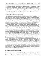
Figure 11.17 PVT aware sleep frequency scheme [12]. (© IEEE 2006)
Another implementation tries to take into account PVT variation to
determine the frequency of entering sleep [12]. It assumes that, for corners
with high leakage, the cache must be more aggressively placed into sleep
mode; for corners with less leakage, the cache can be placed into sleep less
often to reduce active power dissipation. Therefore, as shown in Figure 11.17,
it uses a self-decay circuit to periodically generate the sleep pulse. For
high leakage situations, the circuit would generate sleep pulses much more
frequently, as the leakage power savings outweigh the active power
dissipation. Also, rather than having the sleep signal generated
266 John J. Wuu
periodically, this concept can also be modified to allow cache accesses to
trigger the start of the decay circuit. In such a scheme, the cache would be
placed under sleep if no access to the cache were made after a certain
amount of time, as determined by the self-decay circuit.
11.3.4 Dynamic Cache Power Down
Due to the temporal locality of caches, a line that has not been used for a
long time is not likely to be used again. Therefore, one could power down
portions of a cache that have not been accessed recently. Because those
SRAM cells do not need to retain state, VccMin does not need to be
maintained, potentially realizing additional power savings. In one
conceptual implementation [9], a small binary counter is provided for each
cache line. The counter is clocked by a very slow clock and is reset every
time the cache line is accessed. When the counter saturates, the supply to
the corresponding line is shut off, powering down that line. Such an
implementation requires significant area overhead. In addition, designers
must take care to ensure that the power introduced by the additional
circuitry (e.g., counter, control logic, slow clock) is not greater than the
power savings.
In a different example, a scheme dubbed “cache-by-demand” in a
microprocessor product [16] allows the microarchitecture to dynamically
identify low usage of the cache, then powers down a portion of the cache
to effectively reduce the size of the cache.
11.3.5 Data Bus Encoding
For large caches occupying large die area with wide data words, the active
power dissipated by the long data bus routes could be significant. In such
situations, designers can use data bus encoding for power reduction. Many
encoding algorithms and techniques exist, but this chapterdescribes only
the Bus-Invert Code [5], a simple example, to illustrate the use of data
encoding.
Bus-Invert Code uses one extra bit to store data inversion information.
The design keeps track of the previous data sent over the long wires, and
compares it with the new data. If more than half of the bits are changing
values, then the new data is inverted before being sent to the long wires.
In addition, the inversion bit is set to keep track of the data’s polarity.
Such a scheme reduces the worst case number of transitions to half of the
total number of bits, thus saving worst case power and improving worst
case di/dt. However, savings for typical, random data would be lower, as
Chapter 11 Dynamic and Adaptive Techniques in SRAM Design 267
the percentage of signals changing between two lines of data is typically
much less than 100%.
11.4 Reliability
With caches becoming larger, transistor dimensions getting smaller, and
process variation getting worse, designers must pay careful attention to
reliability, which falls roughly into two categories. The first involves soft
errors, which are errors caused by alpha particle or cosmic ray strikes, and
are transitional in nature. The second type involves hard errors, which
could include latent defects and test escapes.
11.4.1 Soft Errors
Techniques for mitigating soft errors have been widely known for many
years, so this section offers only a brief description. To account for soft
errors, arrays usually require either parity or Error Correcting Code (ECC).
Parity allows for detection of single-bit errors (or, more exactly, an odd
number of errors), but offers no way to correct an error. In other words,
parity turns potential Silent Data Corruption (SDC) into Detected,
Uncorrected Error (DUE). Although this may be sufficient for small
arrays, large arrays generally require ECC. Hamming Code is widely used
in SRAM arrays, which can correct single-bit errors and detect double-bit
errors. Since column multiplexing usually provides physical separation
between neighboring bits in the same ECC word, it becomes very unlikely
for multiple bits in the same ECC word to flip from a single soft error
strike. Therefore, Single-Error-Correct, Double-Error-Detect (SECDED)
codes are generally sufficient for SRAM arrays under typical use.
11.4.2 Hard Errors
Hard errors such as latent defects and test escapes are not detected during
silicon testing, but can surface in the field. Rather than accepting these
failures as true defects, dynamic techniques exist for arrays to tolerate such
failures.
268 John J. Wuu
11.4.2.1 Cache Line Disable
One dynamic technique dynamically disables cache lines by setting the MESI
bits in the tag into a special “never-valid” state when failures are detected
[19]. Once the line enters the “never-valid” state, it will no longer be used
by the processor. Because only a small number of lines are expected to
contain failures, disabling a very small percentage of the overall cache has
negligible impact on performance.
This technique can use different algorithms for determining lines to
disable. For example, when an ECC error is detected, it could rewrite the
corrected line back to the cache and attempt to read the line again. If ECC
error is detected again, then the line is determined to be defective [19].
The drawback to this method, however, is that latent defects often go
through a period of intermittent failures before becoming permanent
defects. During this period, the defect may not remanifest itself while the
corrected data is reread, causing defective lines not to be disabled as early
as possible. Another implementation uses a table to keep track of ECC
failures [4]. When a line causes an ECC failure for the first time, it is
simply corrected, and logged into this table. Since soft errors are not likely
to occur twice in the same line, if ECC error is detected in a line that
already exists in the table, then the failure is determined to be caused by a
defect, and the line is disabled.
11.4.2.2 Cache Line Remap
Another approach to disabling defective lines is by remapping them to
different locations. In [2], a defective line is remapped to a different
column in the same wordline. Since multiple lines now share the same
physical location, the column address is added to the tag bits to
differentiate the lines. During a tag lookup, both the tag and the column
index are compared against the stored tag and column index bits, and a
“hit” is only signaled if both match. This implementation essentially
reduces the size of the cache without disabling any specific addresses.
11.4.2.3 Defect Correction
The cache line disable and remapping techniques discussed above have the
drawback of reducing the actual cache size. Although the impact to
performance could be negligible, these techniques can face other issues.
For example, in applications where determinism is important, these
techniques may pose additional challenges.
By correcting defects rather than disabling defective lines, designers can
avoid such issues. Although ECC is typically used to address soft errors, it
Chapter 11 Dynamic and Adaptive Techniques in SRAM Design 269
could also be used as a powerful tool to correct hard defects. Assuming
the same level of protection against soft errors is required as caches that
use SECDED ECC, such an implementation would require double-error-
correct, triple-error-detect (DECTED) ECC. Out of the two correctable-
error budget, designers can allocate one bit for hard defect correction,
while reserving the other for soft error protection. Under this usage,
designers must always enable correction for at least one error bit to avoid
frequent exceptions for error handling. In applications where soft-error
resiliency is not important, designers could use traditional SECDED ECC
with error correction always enabled.
Such implementations would be able to tolerate one hard defect per
ECC word. In other words, these techniques can correct a very large
number of random, single-bit defects. Since random dopant fluctuation is
expected to be the main limiter to SRAM VccMin as technology continues
to scale, defects at voltages just below VccMin tend to be random, single-
bit failures. Therefore, these error correction features can allow memory
arrays to operate below normal VccMin and help SRAM continue to scale
into future technology nodes.
11.5 Conclusion
This chapter surveyed dynamic and adaptive techniques in the area of
SRAM design that seek to improve read and write margins, reduce power,
and improve reliability.
Dynamic voltage optimization, especially column-based techniques that
can independently improve both read and write margins in a column-
multiplexed design, can be very effective. Silicon results from [22]
demonstrated 10x reduction in random single-bit failures, when applying a
100mV offset from the wordline supply. However, such voltage
optimization techniques can be expensive in product designs. For
example, the area overhead to implement these techniques can be
significant, and supply switching can increase the overall delay. More
importantly, the additional supply can pose many difficulties. A dedicated
second supply to the cache is the most robust solution, but it is costly and
not always available to designers. Other solutions, such as charge sharing,
supply floating, and supply coupling, are risky to design and can have
limitations such as unreliable low frequency operations.
Similar “second-supply” challenges exist for cache sleep techniques as
well. Unless a separate sleep supply is available, the sleep voltage must
be regulated internally via reference voltages or voltage division schemes.
270 John J. Wuu
To account for noise and variation, sufficient margin must be added at
various stages to ensure robust operation across PVT corners. Therefore,
in designs where VccMin is significantly less than VDD, appreciable
power savings can be achieved with cache sleep; however, in designs
where VccMin is close to VDD (e.g., 200mV), realistic power savings may
be limited after taking into account the various voltage margins.
Finally, the ability to tolerate a large number of random bit failures,
either by correction or by other means, can become increasingly important
as SRAM continues to scale. In addition to providing protection against
test escapes and latent defects, which could help lower test time, test
complexity, defect rate in the field, and cost, such features can also lead to
lower VccMin and/or smaller SRAM cells. These features are attractive
because they do not rely on risky circuit design, nor do they require a
separate supply. Rather they are effective architectural features that
designers can implement using known design techniques.
References
[1] Agarwal A, Roy, K (2003) A Noise Tolerant Cache Design to Reduce Gate and
Sub-threshold Leakage in the Nanometer Regime. Proc. ISLPED, pp 18–21
[2] Agarwal A, Paul B, Roy K (2004) A Novel Fault Tolerant Cache to Improve
Yield in Nanometer Technologies. Proc. IOLTS, pp 149–154
[3] Bhavnagarwala A, Kosonocky S, Kowalczyk S, Joshi R, Chan Y, Srinivasan
U, Wadhwa J (2004) A Transregional CMOS SRAM with Single, Logic
VDD and Dynamic Power Rails. Symp. VLSI Circuits Dig. Tech. Papers, pp
292–293
[4] Chang J, Huang M, Shoemaker J, Benoit J, Chen SL, Chen W, Chiu S,
Ganesan R, Leong G, Lukka V, Rusu S, Srivastava D (2007) The 65-nm 16-
MB Shared On-Die L3 Cache for the Dual-Core Intel Xeon Processor 7100
Series. IEEE J. Solid-State Circuits vol 42 no 4, pp 846–852
[5] Cheng W, Pedram M (2001) Memory Bus Encoding for Low Power: A
Tutorial. Proc. ISQED, pp 26–28
[6] Dorsey J, Searles S, Ciraula M, Johnson S, Bujanos N, Wu D, Braganza M,
Meyers S, Fang E, Kumar R (2007) An Integrated Quad-Core Opteron
Processor. ISSCC Dig. Tech. Papers, pp 102–103
[7] International Technology Roadmap for Semiconductors (2001)
[8] Jumel F, Royannez P, Mair H, Scott D, Er Rachidi A, Lagerquist R, Chau M,
Gururajarao S, Thiruvengadam S, Clinton M, Menezes V, Hollingsworth R,
Vaccani J, Piacibello F, Culp N, Rosal J, Ball M, Ben-Amar F, Bouetel L,
Domerego O, Lachese JL, Fournet-Fayard C, Ciroux J, Raibaut C, Ko U
(2006) A Leakage Management System Based on Clock Gating
Infrastructure for a 65-nm Digital Base-Band Modem Chip. Symp. VLSI
Circuits Dig. Tech. Papers, pp 214–215
Chapter 11 Dynamic and Adaptive Techniques in SRAM Design 271
[9] Kaxiras S, Hu Z (2001) Cache Decay: Exploiting Generational Behavior to
Reduce Cache Leakage Power. Int. Symp. Comput. Architect., pp 240–25
[11] Khellah M, Ye Y, Kim NS, Somasekhar D, Pandya G, Farhang A, Zhang K,
Webb C, De V (2006) Wordline & Bitline Pulsing Schemes for Improving
SRAM Cell Stability in Low-Vcc 65nm CMOS Designs. Symp. VLSI
Circuits Dig. Tech. Papers, pp 9–10
[12] Kim C, Kim JJ, Chang IJ, Roy K (2006) PVT-Aware Leakage Reduction for
On-Die Caches With Improved Read Stability. IEEE J. Solid-State Circuits
vol 41 no 1, pp 170–178
[13] Mizuno H, NaganoT (1995) Driving Source-Line (DSL) Cell Architecture
for Sub-1-V High-Speed Low-Power Application. Symp. VLSI Circuits Dig.
Tech. Papers, pp 25–26
[14] Ohbayashi S, Yabuuchi M, Nii K, Tsukamoto Y, Imaoka S, Oda Y,
Yoshihara T, Igarashi M, Takeuchi M, Kawashima H, Yamaguchi Y,
Tsukamoto K, Inuishi M, Makino H, Ishibashi K, Shinohara H (2007) A 65-
nm SoC Embedded 6T-SRAM Designed for Manufacturability With Read
and Write Operation Stabilizing Circuits. IEEE J. Solid-State Circuits vol 42
no 4, pp 820–829
[15] Osada K, Shin JL, Khan M, Liou Y, Wang K, Shoji K, Kuroda K, Ikeda S,
Ishibashi K (2001) Universal-Vdd 0.65-2.0-V 32-kB Cache Using a Voltage-
Adapted Timing-Generation Scheme and a Lithographically Symmetrical
Cell. IEEE J. Solid-State Circuits vol 36 no 11, pp 1738–1744
[16] Sakran N, Yuffe M, Mehalel M, Doweck J, Knoll E, Kovacs A (2007) The
Implementation of the 65nm Dual-Core 64b Merom Processor. ISSCC Dig.
Tech. Papers, pp 106–107
[17] Seevinck E, List FJ, Lohstroh J (1987) Static-Noise Margin Analysis of
MOS SRAM Cells. IEEE J. Solid-State Circuits vol 22 no 5, pp 748–754
[18] Takeyama Y, Otake H, Hirabayashi O, Kushida K, Otsuka N (2006) A Low
Leakage SRAM Macro With Replica Cell Biasing Scheme. IEEE J. Solid-
State Circuits vol 41 no 4, pp 815–822
[19] Wuu J, Weiss D, Morganti C, Dreesen M (2005) The Asynchronous 24MB
On-chip Level-3 Cache for a Dual-core Itanium Family Processor. ISSCC
Dig. Tech. Papers, pp 488–489
[20] Yamaoka M, Shinozaki Y, Maeda N, Shimazaki Y, Kato K, Shimada S,
Yanagisawa K, Osada K (2004) A 300MHz 25uA/Mb Leakage On-Chip
SRAM Module Featuring Process-Variation Immunity and Low-Leakage-
Active Mode for Mobile-Phone-Application Processor. ISSCC Dig. Tech.
Papers, pp 494–495
[21] Yamaoka M, Maeda N, Shinozaki Y, Shimazaki Y, Nii K, Shimada S,
Yanagisawa K, Kawahara T (2006) 90-nm Process-Variation Adaptive
Embedded SRAM Modules With Power-Line-Floating Write Technique.
IEEE J. Solid-State Circuits vol 41 no 3, pp 705–711
[10] Khellah M, Kim SN, Howard J, Ruhl G, Sunna M, Ye Y, Tschanz J,
Somasekhar D, Borkar N, Hamzaoglu F, Pandya G, Farhang A, Zhang K,
De V (2006) A 4.2GHz 0.3mm2 256kb Dual-Vcc SRAM Building Block in
65nm CMOS. ISSCC Dig. Tech. Papers, pp 2572–2573
272 John J. Wuu
[22] Zhang K, Bhattacharya U, Chen Z, Hamzaoglu F, Murray D, Vallepalli N,
Wang Y, Zheng B, Bohr M (2006) A 3-GHz 70-Mb SRAM in 65-nm CMOS
Technology With Integrated Column-Based Dynamic Power Supply. IEEE J.
Solid-State Circuits vol 41 no 1, pp 146–151