Adaptive Techniques for Dynamic Processor Optimization Theory and Practice Episode 2 Part 7 potx
Bạn đang xem bản rút gọn của tài liệu. Xem và tải ngay bản đầy đủ của tài liệu tại đây (1.37 MB, 20 trang )
Chapter 12 The Challenges of Testing Adaptive
Designs
Eric Fetzer, Jason Stinson, Brian Cherkauer, Steve Poehlman
Intel Corporation
In this chapter, we describe the adaptive techniques used in the Itanium® 2
9000 series microprocessor previously known as Montecito [1].
Montecito features two dual-threaded cores with over 26.5 MB of total
on die cache in a 90nm process technology [2] with seven layers of copper
interconnect. The die, shown in Figure 12.1, is 596 mm
2
in size, contains
1.72 billion transistors, and consumes 104 W at a maximum frequency of
1.6 GHz. To manufacture a product of such complexity, a sophisticated
series of tests are performed on each part to ensure reliable operation
throughout its service at a customer installation. Adaptive features often
interfere with these tests. This chapter discusses three adaptive features
on Montecito: active de-skew for reliable low skew clocks, Cache Safe
Technology® for robust cache operation, and Foxton Technology® for
power management. Traditional test methods are discussed, and the
specific impacts of active de-skew and the power measurement system for
Foxton are highlighted. Finally, we analyze different power management
systems and consider their impacts on manufacturing.
12.1 The Adaptive Features of the Itanium 2 9000 Series
12.1.1 Active De-skew
The large die of the Montecito design results in major challenges in
delivering a low skew global clock to all of the clocked elements on the
die. Unintended clock skew directly impacts the frequency of the design
by shortening the sample edge of the clock relative to the driving edge
of a different clock. Random and systematic process variation in both the
A. Wang, S. Naffziger (eds.), Adaptive Techniques for Dynamic Processor Optimization,
DOI: 10.1007/978-0-387-76472-6_12, © Springer Science+Business Media, LLC 2008
274 Eric Fetzer, Jason Stinson, Brian Cherkauer, Steve Poehlman
Figure 12.1 Montecito die micrograph.
transistor and metal layers makes it difficult to accurately design a static
clock distribution network that will deliver a predictable clock edge
placement throughout the die. Additionally, dynamic runtime effects such
as local voltage droop, thermal gradients, and transistor aging further add
to the complexity of delivering a low skew clock network. As a result of
these challenges, the Montecito design implemented an adaptive de-
skewing technique to significantly reduce the clock skew while keeping
power consumption to a minimum.
21.5 mm
27.7 mm
Traditional methods of designing a static low skew network include
both balanced Tree and Grid approaches (Figure 12.2). The traditional
Tree network uses matching buffer stages and either layout-identical metal
routing stages (each route has identical length/width/spacing) or delay-
identical metal routing (routes have different length/width/spacing but
same delay). A Grid network also uses matched buffer stages but creates a
shorted “grid” for the metal routing, where all the outputs of a particular
clock stage are shorted together.
Chapter 12 The Challenges of Testing Adaptive Designs 275
Figure 12.2 Example H-tree and grid distributions.
The benefit of a Tree approach is the relatively low capacitance of the
network compared to the Grid approach. This results in significantly lower
power dissipation. For a typical modern CPU design, the Grid approach
consumes 5–10% of total power, as compared to the Tree approach, which
can be as low as 1–2%. However, the Grid approach is both easier to
design and more tolerant of in-die variation. A Tree network requires very
balanced routes, which take significant time to fine-tune and optimally
place among area-competing digital logic. The Grid network is much
easier to design, as the grid is typically defined early in design and
included as part of the power distribution metallization. The Grid network
is also more tolerant of variation—since all buffers at a given stage are
shorted in a Grid network, variation in devices and metals is effectively
averaged out by neighboring devices/metals. While this results in very low
skew, it also further increases power by creating temporary short circuits
between neighboring skewed buffers. For a fully static network, the Grid
approach is generally the lowest skew approach, but results in a significant
power penalty.
The Montecito design could not afford the additional power
consumption of a Grid approach. An adaptive de-skew system [3] was
integrated with a Tree network to achieve low skew while simultaneously
keeping power to a minimum. The de-skew system compares dozens of
end points along the clock distribution network against their neighbors and
then adjusts distribution buffer delays, using a delay line, to compensate
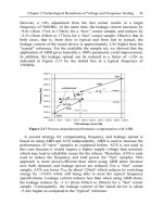
for any skew. Ultimately, a single reference point (zone 53 in Figure 12.3)
is used at the golden measure and all of the other zones (43, 44, etc.) align
to it hierarchically
.
H-tree
Grid
276 Eric Fetzer, Jason Stinson, Brian Cherkauer, Steve Poehlman
Figure 12.3 Partial comparator connectivity for active De-skew. (© IEEE 2005)
Similar de-skewing techniques have been used in past designs [4, 5];
however, these projects have de-skewed the network at startup (power-on)
or determined a fixed setting at manufacturing test. The Montecito
implementation keeps the de-skew correction active even during normal
operation. This has the benefit of correcting for dynamic effects such as
voltage droop and thermal gradient induced skew.
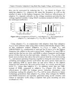
The de-skew comparison uses a circuit called a phase comparator. The
phase comparator (Figure 12.4) takes two clock inputs from different
regions of the die (ina and inb). In the presence of skew, either cvda or
cvdb will rise before the other, which will in turn cause either up or down
to assert. The output of the phase comparator is fed to a programmable
delay buffer to mitigate the skew.
Empirically it has been shown that the adaptive de-skew method on
Montecito decreases the clock skew by 65% when compared to
uncompensated routes. Additionally, using different workloads, the de-
skew network has been demonstrated to help mitigate the impact of
voltage and temperature on the clock skew.
43
44
52
45
46
48
47
Reference Zone: Delay Centered
53
Chapter 12 The Challenges of Testing Adaptive Designs 277
Figure 12.4 Montecito phase comparator circuit. (© IEEE 2005)
12.1.2 Cache Safe Technology
Montecito has a 24 MB last-level cache (LLC) on-die. As a result of its
large size, the cache is susceptible to possible latent permanent or semi-
permanent defects that could occur over the lifetime of the part. The
commonly used technique of Error Correction Codes (ECC) was
insufficient to maintain reliability in the presence of such defects which
significantly add to the multi-bit failure rate. As a result, the design
implements an adaptive technique called Cache Safe Technology (CST) to
dynamically disable cache lines with latent defects during operation of the
CPU.
Like most large memory designs, the Montecito LLC is protected with
a technique called Error Correction Codes (ECC) [6]. For each cache line,
additional bits of information are stored that make it possible to detect and
reconstruct a corrected line of data in the presence of bad bits.
“Temporary” bad cache bits typically arise from a class of phenomenon
collectively called Soft Errors [7]. Soft Errors are the result of either alpha
particles or cosmic rays and cause a charge to be induced into a circuit
node. This induced charge can dynamically upset the state of memory
I
O
I
O
CVD
CVD
VDDVDD
GND
VDD
GND
VDD
cvdacvdb
inb
du
up
ina
down
278 Eric Fetzer, Jason Stinson, Brian Cherkauer, Steve Poehlman
elements in the design. Large caches are more susceptible simply because
of their larger area. Soft Errors occur at a statistically predictable rate
(called Soft Error Rate, or SER), so for any size cache the depth of
protection needed from Soft Errors can be determined. In the case of
Montecito, the LLC implements a single bit correction/double bit detection
scheme to reduce the impact of transient Soft Errors to a negligible level.
The ECC scheme starts to break down in the presence of permanent
cache defects. While the manufacturing flow screens out all initial
permanent cache defects during testing, it is possible for latent defects to
manifest themselves after the part has shipped to a customer. Latent
defects include such mechanisms as Negative Bias Temperature Instability
[8] (NBTI, which induces a shift in V
th
), Hot Carrier or Erratic Bit [9]
(gate oxide-related degradation), and electro-migration (shifts in metal
atoms causing opens and shorts). Montecito implements CST to address
these in-field permanent cache defects.
The CST monitors the ECC events in the cache and permanently
disables cache lines that consistently show failures. At the onset of an in-
field permanent cache defect on a bit, ECC will correct the line when it is
read out. The CST handler will detect that an ECC event occurred and
request a second read from the same cache line. If the bit is corrected on
the second read, the handler will determine that the line has a latent defect.
The data is moved to a separate area of the cache, and CST marks the line
as invalid for use. The line remains invalid until the machine is restarted.
In this manner, a large number of latent defects can be handled by CST
while using ECC only to handle the temporary bit failures of Soft Errors.
12.1.3 Foxton Technology
Montecito features twice the number of cores of its predecessor and a large
LLC, yet it reduces total power consumption to 104W compared to 130W
for its predecessor. This puts the chip under very tight power constraints.
By monitoring power directly, Montecito can adaptively adjust its power
consumption to stay within a specified power envelope. It does this
through a technique called Foxton Technology [10]. This prevents
overdesign of the system components such as voltage regulators and
cooling solutions, while reducing the guard-bands required to guarantee
that a part stays within the specification. Foxton Technology
implementation is divided into two pieces: power monitoring and reaction.
Chapter 12 The Challenges of Testing Adaptive Designs 279
Power monitoring is accomplished through a mechanism that measures
both voltage and resistance to back calculate the current. If the resistance
of a section of the power delivery is known (R
pkg
), and the voltage drop
across that resistance is known (
dieconn VV − ), then power can be calculated
simply as:
()
pkg
dieconndie
R
VVV
Power
−
=
*
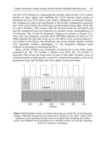
Power is delivered to the Montecito design by a voltage regulator, via an
edge connector, through a substrate on which the die is mounted.
Figure 12.5 Montecito package.
The section of power delivery from the edge connector (Figure 12.5) to
the on-die grid is used as the measurement point to calculate power.
Montecito has four separate supplies (Vcore, Vcache, Vio, and V
fixed
),
which all need to be monitored or estimated in order to keep the total
power below the specification.
Edge
Connector
Die
(Under heat spreader)
280 Eric Fetzer, Jason Stinson, Brian Cherkauer, Steve Poehlman
Figure 12.6 Measurement block diagram.
To calculate the voltage drop, the voltages at the edge connector and on-
die grid need to be measured. A voltage-controlled ring oscillator (VCO) is
used to provide this measurement (Figure 12.6). The higher the voltage,
the faster the VCO will transition. By attaching a counter to the output of
the VCO, a digital count can be generated that is representative of the
voltage seen by the VCO. To convert counts to voltages, a set of on-die
reference voltages are supplied to the VCO to create a voltage-to-count
lookup table. Once the table is created, voltage can be interpolated
between entries in the lookup table. Linearity is critical in this
interpolation—the VCOs are designed to maintain strong linearity in the
voltage range of interest. Dedicated low resistance trace lines route the
two points (edge connector voltage and on-die voltage) to the VCOs on the
microprocessor.
To calculate the resistance,
R
pkg
, a special calibration algorithm is used.
Because package resistance varies both from package to package and with
temperature, the resistance value is not constant. Using on-die current
sources to supply known current values, the calibration runs periodically to
compute package resistance. By applying a known current across the
resistance, and measuring the voltage drop, the resistance can be
calculated.
Once the power is known, the Montecito design has two different
mechanisms to adjust power consumption to stay within its power
specification. The first is an architectural method, which artificially
throttles instruction execution to reduce power. By limiting the number of
instructions that can be executed, the design will have less activity and
hence lower power. Aggressive clock gating in the design (shutting off the
clock to logic that is not being used) is particularly important in helping to
reduce power when instruction execution is throttled.
The second method of power adjustment dynamically adjusts both the
voltage and frequency of the design. If the power, voltage, and frequency
Counter
VCO
1
Voltages
to be
measured
Count
Chapter 12 The Challenges of Testing Adaptive Designs 281
of the current system are known, it is a simple matter to recalculate the
new power when voltage and frequency are adjusted. A small state
machine called a charge-rationing controller (QRC) is provided in the
design to make these calculations and determine the optimal voltage and
frequency to adhere to the power specification. The voltage regulator used
with the Montecito design can be digitally controlled by the processor,
enabling the voltage to be raised and lowered by the QRC. The on-die
clock system also has the ability to dynamically adjust frequency in
increments of 1/64th of a clock cycle. Using this method, the QRC can
control both the frequency and voltage of the design in real time, enabling
it to react to the power monitoring measurements. This second mechanism
was used as a proof of concept on the Montecito design and is expected to
be utilized in future designs.
12.2 The Path to Production
12.2.1 Fundamentals of Testing with Automated Test
Equipment (ATE)
All test methods rely on two fundamental properties of the content and
automatic test equipment environments: determinism and repeatability.
Determinism is the ability to predict the outcome of a test by knowing the
input stimulus. Determinism is required for defect-free devices to match
the logic simulation used to generate test patterns. Repeatability is the
ability to do the same thing over and over and achieve the same result.
This is not same as determinism in that it does not guarantee that the result
is known. In testing, given the same electrical environment (frequency,
voltage, temp, etc.), the same results should be achievable each and every
time a test runs passing or failing.
12.2.2 Manufacturing Test
Manufacturing production test is focused on screening for defects and the
determination of the frequency, power, and voltage that the device
operates at (a process known as “binning”) (Figure 12.7). Production
testing is typically done in three environments [11, 12].
282 Eric Fetzer, Jason Stinson, Brian Cherkauer, Steve Poehlman
Figure 12.7 Test flow.
The first of these environments is wafer sort. Wafer sort is usually the
least “capable” test environment as there are limitations in what testing can
be performed through a probe card, as well as thermal limitations [13,12].
Power delivery and I/O signal counts for most modern VLSI designs
exceed the capabilities of probe cards to deliver full functionality. With
these limitations, wafer testing is usually limited to power supply shorts,
shorts and opens on a limited number of I/O pads and basic functionality.
Basic functionality testing is performed through special test modes and
“backdoor” features that allow access to internal state in a limited pin
count environment. This type of testing is referred to as “structural test”
and is distinguished from “functional test”, which uses normal pathways to
test the device. Structural testing is typically focused on memory array
structures and logic. The arrays are tested via test modes that change the
access to the cache arrays to enable testing via BIST (built-in-self-test) or
DAT (direct access testing, where the tester can directly access the address
and data paths to an array). Logic is often tested using scan access to
apply test patterns generated by ATPG (automated pattern generation)
tools and/or BIST.
Fabrication
Wafer Sort
Burn-in
Packaging
Class
System
Screen/
Binning
Points
Chapter 12 The Challenges of Testing Adaptive Designs 283
12.2.3 Class or Package Testing
After dice which pass wafer sort have been assembled, they are passed
through burn-in, which operates the part at high voltages and temperatures
revealing defects in manufacture while stabilizing device characteristics.
The next test step is called class testing, or package test. The package
enables fully featured voltage, frequency, and thermal testing of the
processor—this is known as “functional testing”. Class testers and device
handlers are very complex and expensive pieces of equipment that handle
all of the various testing requirements of a large microprocessor. Power
delivery, high speed I/O, large diagnostic memory space, and thermal
dissipation requirements significantly drive up cost and complexity of a
functional tester.
The tester and test socket need to be able to meet all power and thermal
delivery needs to fully test to the outer envelope of the design
specifications, and thus meet or exceed any real customer system
environments. This includes frequency performance testing to determine
if the processor meets the “binning” frequency. A common practice for
processor designs is to support multiple frequency “bins”, which takes
advantage of natural manufacturing variation by creating multiple
variations of a product that are sold at different frequencies. The class
socket is the primary testing socket used to determine the frequency bin to
which a given part should belong. Frequency testing allows for screening
of speed-sensitive defects as well as any electrical marginality that may
exist as a result of the design or manufacturing process. In addition to
frequency binning, binning based on power requirements is also becoming
a common practice with today’s high-performance processors due to
customer demands for more power efficient products.
While wafer sort does not typically support full pin counts or full
frequency testing, the class socket is fully featured for both. The class
socket environment supports large pin counts and the high frequencies
needed to test the processor at full input/output requirements, and provides
the needed power connections to the power supplies in the tester. Support
for the full complement of processor pins allows for normal functional
testing (running code) in the class socket.
Traditional test pattern content is generated by simulating the case on a
functional logic model [14]. The test case is simulated using the logic
model for the processor, and the logic values at the pads are captured for
each bus clock cycle during the simulation. The captured simulation data
is then post-processed into a format which the tester can use to provide the
stimulus and the expected results for testing of the processor. The
operation of the processor in the tester socket must be deterministic and
284 Eric Fetzer, Jason Stinson, Brian Cherkauer, Steve Poehlman
match the simulation environment exactly to enable the device under test
to pass. As the expected data is stored in the tester and is compared at
specific clock cycles relative to the stimulus data, this is called “stored
response” testing (Figure 12.8). This is distinguished from “transaction”
testing, which does not require cycle accurate deterministic behavior.
Transaction testing usually requires an “intelligent” agent to effectively
communicate with the device under test in its own functional protocol—
this is usually accomplished through the use of another IC (e.g., a chipset)
or a full system. Transaction testing at the class socket is still in early
development phases within the industry—currently this type of testing is
usually reserved for the final socket (system-based).
Figure 12.8 Stored response tester interface.
In recent years, cache resident testing has become more popular
[15,16,13,17] for microprocessors. The test case is loaded into the
processor’s internal caches and then executed wholly from within the
cache memory. The execution of the test case must use only the state
internal to the processor to pass—there can’t be any reliance on the
external bus or state that wasn’t preconditioned when the test case was
loaded. Test cases are written in such a manner that they produce a
passing signature, which is then stored in either a register or cache memory
location. If the expected signature isn’t read out correctly at the end of the
test case, the processor has failed the test pattern and is deemed a “failure”.
The expected “signature” can be developed in several ways. One
approach is to preload the test case into the logic simulator and run it to
completion. At the end of the simulation, the “signature” for the test case
is recorded. As the case is simulated on the logic model, the “signature”
can contain cycle-accurate timing for all signals. This enables the
Drive
Data Bus
ZZZZ ZZZZ
ZZZZ ZZZZ
9090 9090
9090 9090
ZZZZ ZZZZ
ZZZZ ZZZZ
9090 9090
9090 90F4
ZZZZ ZZZZ
Expect
Addr Bus
FFFF FFB0
FFFF FFB0
XXXX XXXX
XXXX XXXX
FFFF FFC0
FFFF FFC0
XXXX XXXX
XXXX XXXX
FFFF FFD0
Acquire
Addr Bus
FFFF FFB0
FFFF FF
C
0
FFFF FF
C
0
FFFF FF
C
0
FFFF FF
D
0
FFFF FF
D
0
FFFF FF
D
0
FFFF FF
D
0
0000 0010
Chapter 12 The Challenges of Testing Adaptive Designs 285
resulting test to not only check for architecturally correct behavior but also
timing correct behavior—for instance, that the test completed within a
specific number of core cycles. However, the cost of this level of timing
accuracy is very slow simulation speeds through the logic model.
Ultimately, simulation speed will limit the size and complexity of tests that
take this approach.
A second approach to determine the “signature” is to code in the
expected result. The test case only has to be valid assembly code that can
be compiled into a format usable by the cache and initialization code.
Without the use of logic simulation, care must be taken to prevent the
inclusion of any clock cycle-dependent signals. This method of signature
generation enables architectural validation, but not cycle-accurate timing
validation. The benefit of this approach is that very large, complex
diagnostics can be developed since they aren’t dependent on very slow
logic model simulations. Much faster architectural-level simulators may be
used to compute the final “signature”. Additionally, this approach enables
non-deterministic architectural features to be tested. For instance, power
management features that dynamically change the bus ratio based on
power and/or thermal values are not deterministic because of the random
nature of such values. This approach enables testing of such non-
deterministic features.
12.2.4 System Testing
Platform or system testing provides flexibility not available in either the
wafer sort or class tester environments. With the added flexibility comes
higher cost and complexity, as the “tester” must be instrumented to
determine when failures occur. The system test is transaction based—
meaning that it intelligently communicates with the device under test
rather than simply driving inputs and comparing outputs based on a
predetermined set of vectors (stored response). This enables significantly
longer tests compared to the class testers as only the transactions need to
be stored in memory. In a stored response test, every single bus cycle of
input and output data needs to be stored in memory. This makes the system
test socket much more flexible in terms of the test content that can be used
to test the device. However, with the flexibility comes less controllability
and observability of the device under test. This makes it more difficult to
determine pass/fail conditions as well as direct the test diagnostics at
specific conditions or areas of the design.
There are two basic methods of checking pass/fail used for system test.
The first is to use a “golden” device that subsequent devices under test are
286 Eric Fetzer, Jason Stinson, Brian Cherkauer, Steve Poehlman
compared against. This is done by developing a custom system that allows
for both the golden device and the device under test to receive the same
stimulus from the system, and the golden device controls the system via its
outputs that are compared to the device under test. If any differences
occur, the device under test becomes a failed part and thus is no longer a
candidate to be shipped to the customer. This approach has the limitation
that all “good” devices must perform in exactly the same way as the
golden device. With modern power management schemes and control, it is
no longer true that all “good” devices perform in exactly the same way.
The second approach is to develop test content that is self-checking.
This means that the content must test the desired functionality in such a
way to produce a passing signature in memory or internal cache location.
A system controller will examine the test pattern result and determine if it
is passing or failing.
The test system controller must monitor power supply voltages, current,
and temperature of the processor under test to determine if the device is
performing within the required specifications. Thus, the system controller
must have an additional level of automation and monitoring beyond just
the test pattern content control. This adds to the overall cost and
complexity of the system test step. Similar to the class test and wafer sort,
the system test will follow a preprogrammed step of operations and
decision tree to “bin” the processor. These steps will take longer than on
the class tester because the test cases have less controllability and
observability and must run longer to achieve similar design coverage.
Also, the overhead of communicating with other devices external to the
system adds significantly to the test time. However, the lower cost of a
system test (relative to class test) combined with the ability to run very
long diagnostic content actually enables this socket to provide the highest
test coverage. Also, since system test does not require cycle-accurate
determinism, it’s the ideal location to test non-deterministic architectural
features such as power and thermal management.
12.3 The Impact of Adaptive Techniques on Determinism
and Repeatability
Adaptive circuits can impact both determinism and repeatability when
testing and validating systems. Adaptive systems will often behave
differently at different times. These differences negatively impact
automated systems for observing chip behavior.
Chapter 12 The Challenges of Testing Adaptive Designs 287
For instance, active clock de-skewing, when directly observed, will
generate a unique and unpredictable result. At any moment in time small
voltage fluctuations or thermal variations can cause the state of the system
to have an apparently random value. When observed, these values will
appear to be non-deterministic (unpredictable) and non-repeatable
(different on each run). Without special consideration, direct observations
of the active de-skew state would not be usable for manufacturing test.
As previously described, the Foxton power management system can
dynamically adjust frequency to control power. Such changes in
frequency can cause the chip to execute code over more cycles to reduce
power. If this behavior is activated during traditional ATE testing, the
tests will come back as failures since the ATE expects results to be cycle
accurate.
The next few sections describe the validation and testing of these two
features, active de-skew and Foxton technology, on the Itanium 2
processor and the techniques used to resolve the determinism and
repeatability issues.
12.3.1 Validation of Active De-skew
The validation of the active de-skew system took many brute force
methods. The first step in validating the de-skew system is measuring the
behavior of the delay line, which is used to adjust the delay of the clock
buffers. To do this, fixed delay line trim control values were scanned into
the delay line to characterize delay line performance for a given setting.
The impact to the delay was measured using an oscilloscope connected to
a clock observability output pin on the processor package. The tick size
for each of the 128 settings is about 1.5 ps. To achieve this resolution in
measurement, tens of thousands of samples needed to be taken for each
data point. Figure 12.9 shows the results from a typical part. Notice the
inflection points that can be found at settings 32 and 96. These indices,
along with setting 64, represent transition points inside the circuit. The
inflections are caused by the slight additional capacitive load from routing
in the layout. Setting 64, being the center point of the design, was better
matched than 32 and 96 and as a result has a smaller deviation. This extra
capacitance slows down the edge rate and increases the impact of
particular trim settings.
288 Eric Fetzer, Jason Stinson, Brian Cherkauer, Steve Poehlman
Figure 12.9 Active de-skew buffer linearity. (© IEEE 2005)
To check the comparator outputs (Figure 12.4) “up” and “down” that
control the delay line in normal operation, the delay line can be scanned to
each possible value. As the delay line value is increased, the comparator
output changes (representing the changing relationship of the clocks). The
comparator output can be viewed directly via scan and must be monotonic
for the de-skew system to work.
Verification of the delay line and comparators in isolation doesn’t prove
that the active de-skew system actually removes skew. Measuring CPU
frequency with the de-skew system on and off gives an indication of
operation but is still not sufficient. It is possible, and probable, that a critical
timing path (a circuit whose performance limits die frequency) can actually
be improved by skew. In this case, active de-skew could actually slow down
a part. To prevent this situation, the system has the ability to add fixed
offsets that can be introduced via firmware to improve these paths.
To determine if active de-skew is removing skew appropriately, a more
direct approach was necessary. Through the use of optical emission
probing [18], it is possible to measure delays in the clock distribution
accurately. Figure 12.10 shows a waveform of emitted light intensity for
Inflection
Points
Chapter 12 The Challenges of Testing Adaptive Designs 289
several different clock drivers across the die, which is indicative of the
clock distribution delay to each of the drivers. With de-skew off, a
selected clock trace exhibits significant skew. With de-skew on; the
particular clock trace is in the middle of the pack. While Figure 12.10
only shows a single outlier to represent the range of skews observed, a
complete population of clocks would show a full spectrum of delays
between the earliest and latest waveforms representing the total skew. The
optical probing infrastructure inhibits heat removal, so absolute skew
measurements using this method are not reliable representations of skew
for a normal CPU. Such probing is very time consuming and can only be
performed on a few parts. Probing did reveal that skew found with de-
skew off in one core was not necessarily in the other core. Since the cores
are identical in layout and simply mirrored, the only possible differences
between them are process, voltage, and temperature variations.
Figure 12.10 Light emission waveforms for clock drivers. (© IEEE 2005)
While these methods of verifying the behaviors of active de-skew are
appropriate for small numbers of parts, they are not feasible for volume
production testing. Oscilloscope measurements and optical probing can
De-skew Disabled
De-skew Enabled
290 Eric Fetzer, Jason Stinson, Brian Cherkauer, Steve Poehlman
require several hours per part to perform the measurements. Furthermore
optical probing requires part disassembly to observe the photons. As a
result, different solutions were required for volume testing in production.
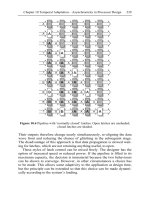
12.3.2 Testing of Active De-skew
As discussed earlier, direct observation of values to be compared on a
tester generally have to be repeatable and deterministic. To get around this
limitation in ATE, codes can be used to create tester detectable patterns.
This data is not checked as the test is running, but instead the data is
collected by the tester for further analysis. In the case of active de-skew,
thermometer codes were used to evaluate the correctness of the delay line
trim settings. Typically, the delay line would store the trim setting in a
binary value. For 128 possible settings, this would only require 7 bits to
store. However, with data stored in this manner, if one of the bits is
wrong, how would it be detected? Since there is no expected, known value
to compare against, there is no way to determine whether the observed
value reflects correct operation. By using a thermometer code, at the
expense of 121 extra storage elements, the integrity of the code can be
checked by the tester. In the example in Figure 12.11, a single error in the
code shows up as a second 0 to 1 transition in the thermometer code. By
intentionally skewing the inputs to comparators in the de-skew system,
functionality can be checked for all possible clock relationships and delay
line values.
0011001 0011011
Binary Encoded Value (7 bits Required)
Thermometer Encoded Value (128 bits Required)
Undetectable
Error
Error
Identified by
multiple
0Æ1
transitions
Desired Observed
Desired Observed
00011111 …00010111…
00011111 …01
011111…
0011001 001101
1
Binary Encoded Value (7 bits Required)
Thermometer Encoded Value (128 bits Required)
Undetectable
Error
Error
Identified by
multiple
0Æ1
transitions
Desired Observed
Desired Observed
00011111 …00010111…
00011111 …01
011111…
Figure 12.11 Thermometer code example.
Chapter 12 The Challenges of Testing Adaptive Designs 291
Testing the rest of the chip with clock de-skew operating also has
challenges. One technique for testing circuits is to stop the clock, scan in a
test vector, burst the clock for a few cycles, and scan out a result. This
method of testing has many direct conflicts with active de-skew.
• Stopping the clock prevents the active de-skew system from updating
properly. Without updates, the active de-skew system will not
compensate for skew that results from changing environmental
conditions during testing.
• If the clock skew, while in a system, is not the same as the skew during
testing by ATE, the manufacturing test can end up being an inaccurate
measurement of actual processor speed in a system.
• Stop clock conditions create voltage overshoot/droop events that do not
exist while clocks are continuously operating.
As a result, special consideration must be taken when testing using this
method. The de-skew system must be preloaded with fixed values during
ATE testing that represent skew conditions in the system. The de-skew
system must also be disabled while actually running the test to prevent a
response to the “artificial” voltage event that results from this kind of test.
12.3.3 Testing of Power Measurement
Central to Montecito’s Foxton power management system is the ability to
measure power consumed at any given moment. The power measurement
system utilizes a small microcontroller, an input selectable VCO (voltage
controlled oscillator) and the natural parasitic resistance of the package, as
described earlier. Testing power measurement requires ensuring that each
individual component is within the required specifications.
The power microcontroller, unlike the other parts of the microprocessor,
runs at its own fixed frequency. While the processor can dynamically
change frequencies, the power controller needs a constant known
frequency for its understanding of time. As a result, all communication
between the microcontroller and the rest of the processor is asynchronous.
In order to test the microcontroller directly, a BIST engine and custom test
patterns are used. Due to its asynchronous nature when communicating
with the core, and its non-deterministic outputs when measuring power,
testing the microcontroller at speed is more involved than simply running
code on the processor and checking its results. To test the microcontroller
features, its firmware is replaced with special self-checking content. This
content is run and stores its results which are then scanned out using cache
resident structural test content as described previously.
292 Eric Fetzer, Jason Stinson, Brian Cherkauer, Steve Poehlman
In a normally functioning system, the VCO counts are calibrated to
known voltages by using a band-gap reference on the package and a
resistor ladder on the die (Figure 12.12). The microcontroller samples the
VCO count for each voltage, V
ladder
, available from the resistor ladder.
Figure 12.12 VCO calibration circuit diagram.
To perform a measurement, the firmware receives a count from the VCO
and interpolates between the two nearest datapoints. Using Table 12.1, it
can be seen how a count of 19350 would be translated into a voltage of
1.018V through interpolation.
Table 12.1 Voltage vs. VCO count example.
Voltage Count
(example)
1.000 19250
1.007 19291
1.015 19337
1.023 19375
1.030 19410
Counter
VCO
Bandgap
Voltage
Ref.
3.3V
1
Voltage
Ladder
Package Die