Microsensors, MEMS and Smart Devices - Gardner Varadhan and Awadelkarim Part 9 ppt
Bạn đang xem bản rút gọn của tài liệu. Xem và tải ngay bản đầy đủ của tài liệu tại đây (2.25 MB, 30 trang )
APPLICATIONS
223
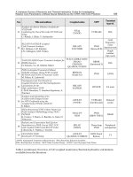
Table
7.2
Technical specification
of
microvalves
350-
300-
250-
200-
150-
100-
50-
0-
-50
-100
Valve
part
Value
Valve
chamber size (mm)
Valve
chamber material
Fluid
chamber size (mm)
Actuator chamber size (mm)
Inlet opening diameter (um)
Membrane diameter (mm)
Membrane thickness (urn)
Membrane material
Membrane deflection (um)
Maximum
flow
rates
and
inlet
pressure
Lifetime
(load cycles)
5
x 5 x 1
PMMA
Diameter
3,
height 0.125
Diameter
3,
height 0.125
100
3
25
Polyimide
120
max.
0.49 m//s
at 740 hPa
>285
million
Actuator
pressures
to
close
the
valve
Actuator
pressures
to
open
the
valve
^
- /^ - • •- *
0
100
600 700
700 800
200
300 400 500
Inlet
pressure (hPa)
(a)
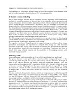
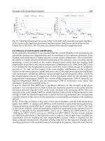
Figure
7.67
Characteristics
of a
microvalve fabricated
by the
AMANDA
process:
(a)
actuation
pressure
and (b)
volumetric
flow
rate
data
on
these microvalve samples
are
listed
in
Table
7.2 and the
measured characteristics
of
the
microvalve
are
presented
in
Figure 7.67. Applications include integral components
of
pneumatic
and
hydraulic systems, systems
for
chemical
analyses
of
liquids
and
gases,
dosage systems
for
medical applications,
and so on.
AMANDA
has
also been used
to
fabricate transducers.
For
polymer membranes,
the
low
Young's modulus results
in
large
deflections
and
strains
at
comparatively
low
pressure
loads. Therefore, polymer pressure transducers
are
suitable
for
measuring small differential
pressures.
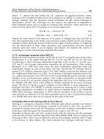
A
schematic view
of a
pressure transducer
is
shown
in
Figure 7.68 (Martin
et
al.
1998);
the
outer dimensions
of
this transducer
are 5.5 x 4.3 x 1.2
mm
3
.
The
thin
polyirnide
diaphragm supports strain gauges made
of
gold, covered
by a 30
um-thick
polyimide disk. This disk bends
by the
pressure dropped across
the
diaphragm,
and the
generated strain
is
measured
with
a
Wheatstone bridge.
A
volume
flow
transducer based
on
pressure
difference
measurement
is
shown
in
Figure 7.69 (Martin
et al.
1998).
The
pressure
drop
along
a
capillary
is
measured
and
the
flow
rate
is
then calculated. These transducers
can be
easily integrated into
the
polymer
micropump
and
microvalves developed
by the
AMANDA process
to
form
a
fully
integrated microfluidic system.
224
MICROSTEREOLITHOGRAPHY
FOR
MEMS
Figure
7.68
(a)
Schematic cross section
of a
differential
pressure transducer
and (b) top
view
of
the
polyimide plate
and
strain gauge pattern
Figure 7.69 Schematic cross section
of a
volumetric
flow
rates transducer
without
electrical
contacts.
From Martin
et al.
(1998)
7.10 CONCLUDING REMARKS
In
this chapter,
we
have reviewed
the
emerging
field of MSL and its
combination with
other
process
technologies.
MSL
offers
the
promise
of
making
a
variety
of
microparts
and
microstructures
without
the use of
vacuum
systems and,
in the
case
of
polymeric
microparts, high temperatures.
It is
particularly attractive
in
that
it can be
used
to
make
in
batch
process
truly
3-D
microparts
in a
wide range
of
materials, polymers, metals,
and
ceramics
at a
modest cost. Because there
are
many
applications
in
which
silicon
microstructures
are
ruled
out as a
result
of, for
example, biocompatibility, this technology
looks
extremely promising,
not
only
for
biofluidic
but
also
for
other types
of
MEMS
REFERENCES
225
devices.
The
main
disadvantage
of MSL is
that
it
takes
a
long
time
to
write
into,
and
process,
a
large
number
of
resist
layers
to
fabricate
a 3-D
component.
Although
some
of
the
MSL
process
technologies
address
this
issue,
costs
must
be
reduced
to
compete
with
simpler
methods,
such
as
stamping,
making
2-D
microstructures.
REFERENCES
Andre,
J. C., Le
Methanute,
A. and de
Wittee,
O.
(1984). French Patent,
No.
8411241.
Ballandras,
S. et al.
(1997). "Microstereolithography
and
shape memory alloy
for the
fabrication
of
miniaturised actuators," Sensors
and
Actuators
A, 62,
741–747.
Bau,
H. H. et al.
(1998). "Ceramic tape-based meso systems technology," ASME MEMS,
66.
491–498.
Beluze,
L.,
Bertch,
A. and
Renaud,
P.
(1999). "Microstereolithography:
a new
process
to
build
complex three-dimensional objects," Proc. SPIE,
3680,
808–817.
Bernard,
W. L.,
Kahn,
H.,
Heuer,
A. H. and
Huff,
M. A.
(1997).
"A
titanium-nickel-shape-memory
alloy
actuated micropump," IEEE Technical Digest
on
Transducers '97,
1,
361–364.
Bertsch,
A.,
Lorenz,
H. and
Renaud,
P.
(1998). "Combined microstereolithography
and
thick resist
UV
lithography
for
three-dimensional microfabrication," Proc. IEEE MEMS, 1823.
Bertsch,
A. et al.
(1997). "Microstereolithography using liquid crystal display
as
dynamic mask-
generator," Microsyst. Technoi,
3,
42–47.
Cabrera,
M. et al.
(1998). "Microphotofabrication
of
very small objects: pushing
the
limits
of
stereolithography," Mol. Cryst. Liq. Cryst., 315, 223–234.
Cohen,
A. et al.
(1999). "EFAB: rapid, low-cost desktop micromachining
of
high aspect ratio true
three-dimensional
MEMS,"
Proc. IEEE MEMS, 244–251.
Corrozza,
M. C.,
Croce,
N.,
Magnani,
B. and
Dario,
P.
(1995).
"A
piezoelectric-driven
stereolithography-fabricated micropump,"
J.
Micromech. Microeng.,
5,
177–179.
English,
J. M. and
Allen,
M. G.
(1999). "Wireless micromachined ceramic pressure sensors," Proc.
12th
IEEE
Int.
Conf.
Microelectromech. Syst., 511–516.
Epstein,
A. H. et al.
(1997). Proc. Int.
Conf.
Solid-State Sensors
Actuators,
2,
753–756.
Griffith,
M. L. and
Halloran,
J. W.
(1995). "Stereolithography
of
ceramics,
"
Proc. 27th Int.
SAMPE
Technical
Conf.,
970–979.
Hull,
C.
(1984).
US
Patent
No.
4,575, August
8,
330.
Ikuta,
K. and
Hirowatari,
K.
(1993). "Real three-dimensional microfabrication using stereolithog-
raphy
and
metal molding," Proc. IEEE MEMS, 42–47.
Ikuta,
K.,
Maruo,
S. and
Kojima,
S.
(1998).
"New microstereolithography
for
freely
moved three-
dimensional
microstructure-super
IH
process
with
submicron resolution," Proc. IEEE MEMS,
290–295.
Ikuta,
K.,
Maruo,
S.,
Fujisawa,
T. and
Yamada,
A.
(1999).
"Microconcentrator
with
opto-sense
microreactor
for
biomedical
IC
chip family," Proc. IEEE MEMS, 376–381.
Ikuta,
K.,
Ogata,
T.,
Tsubio,
M. and
Kojima,
S.
(1996). "Development
of
mass productive
microstereolithography (mass-IH
process),"
Proc. IEEE MEMS,
301–305.
Jacobs,
P. F.
(1992). Rapid prototyping
and
manufacturing: fundamentals
of
stereolithography,
Society
of
Manufacturing
Engineers, USA.
Jacobs,
P. F.
(1996) Stereolithography
and
other RP&M technologies:
from
rapid
prototyping
to
rapid
tooling. Society
of
Manufacturing
Engineers, USA.
Jiang,
X. N. et al.
(1998). "Micronozzle/diffuser
flow and its
application
in
micro-valveless pump,"
Sensors
and
Actuators
A, 70,
81–87.
Jiang,
X. N.,
Sun,
C. and
Zhang,
X.
(1999). "Microstereolithography
of
three-dimensional complex
ceramic
microstructures
and PZT
thick
films on Si
substrate," ASME MEMS,
1,
67–73.
226
MICROSTEREOLITHOGRAPHY
FOR
MEMS
Katagi,
T. and
Nakajima,
N.
(1993).
"Photoforming applied
to fine
machining,"
Proc.
IEEE
MEMS,
173–178.
Kathuria,
Y. P.
(1996).
"Rapid prototyping:
an
innovative technique
for
microfabrication
of
metallic
parts,"
Proc.
7th
Int.
Symp.
Micromachine Hum.
Sci.,
59–65.
Kodama,
H.
(1981). "Automatic method
for
fabricating
a
three-dimensional plastic model
with
photo-hardening polymer,"
Rev. Sci.
Instrum.,
52,
1770–1773.
Madden,
J. D. and
Hunter,
J. W.
(1996). "Three-dimensional microfabrication
by
localised
electro-
chemical deposition,"
J.
Microelectromech. Syst.,
5,
24–32.
Martin,
J.,
Bacher,
W.,
Hagena,
O. F. and
Schomburg,
W. K.
(1998). "Strain gauge pressure
and
volume-flow
transducers made
by
thermoplastic molding
and
membrane transfer, "Proc.
IEEE
MEMS,
361–366.
Maruo,
S. and
Kawata,
S.
(1998).
'Two-photon-absorbed
near-infrared photopolymerisation
for
three-dimensional microfabrication,"
J.
Microelectromech. Syst.,
7,
411–415.
Maruo,
S. and
Kawata,
S.
(1997). "Two-photon-absorbed photopolymerisation
for
three-
dimensional
microfabrication," Proc.
IEEE
MEMS, 169–174.
Monneret,
S.,
Loubere,
V. and
Corbel,
S.
(1999). "Microstereolithography using
a
dynamic mask
generator
and
noncoherent visible light source," Proc. SPIE,
3680,
553–561.
Nakamoto,
T. and
Yamaguchi,
K.
(1996).
"Consideration
on the
producing
of
high
aspect
ratio
microparts using
UV
sensitive photopolymer," Proc.
7th
Int.
Symp.
Micromachine Human
Sci.,
53–58.
Polla,
D. L. and
Francis,
L. F.
(1996).
"Ferroelectric
thin
films in
microelectromechanical systems
applications,"
MRS
Bull.,
59–65.
Schomburg,
W. K. et al.
(1998). "AMANDA-low-cost production
of
microfluidic
devices," Sensors
and
Actuators
A, 70,
153-158.
Sun,
C.,
Jiang,
X. N. and
Zhang,
X.
(1999). "Experimental
and
numerical study
on
microstereo-
lithography
of
ceramics,"
ASME MEMS,
339–345.
Suzumori,
K.,
Koga,
A. and
Haneda,
R.
(1994). "Microfabrication
of
integrated FMAs
using
stereo-
lithography," Proc.
IEEE
MEMS,
136–141.
Takagi,
T. and
Nakajima,
N.
(1994). "Architecture combination
by
micro photoforming
process,"
Proc.
IEEE
MEMS, 211–216.
Taylor,
C. S. et al.
(1994).
"A
spatial
forming
a
three-dimensional printing
process,"
Proc.
IEEE
MEMS,
203-208.
Thornell,
G. and
Johansson,
S.
(1998). "Microprocessing
at the fingertips," J.
Micromech.
Microeng.,
8,
251–262.
Varadan,
V. K.,
Varadan,
V. V. and
Motojima,
S.
(1996).
"Three-dimensional polymeric
and
ceramic
MEMS
and
their
applications,"
Proc. SPIE,
2722,
156–164.
Wayne,
R. P.
(1988). Principles
and
Applications
of
Photochemistry, Oxford
University
Press,
New
York.
Zhang,
X.,
Jiang,
X. N. and
Sun,
C.
(1999). "Microstereolithography
of
polymeric
and
ceramic
microstructures," Sensors
and
Actuators
A, 77,
149–156.
`Zissi,
S. et al.
(1996). "Stereolithography
and
microtechnologies," Microsyst. Technol.,
2,
97–102.
8
Microsensors
8.1
INTRODUCTION
A
sensor
may be
simply
defined
as a
device that converts
a
nonelectrical input
quantity
E
into
an
electrical output signal
E;
conversely,
an
actuator
may be
defined
as a
device that
converts
an
electrical signal
E
into
a
nonelectrical quantity
E
(see Figure 8.1).
In
contrast,
a
processor modifies
an
electrical signal (e.g. amplifies,
conditions,
and
transforms)
but
does
not
convert
its
primary
form.
A
transducer
is a
device that
can be
either
a
sensor
or
an
actuator. Some devices
can be
operated both
as a
sensor
and an
actuator.
For
example,
a
pair
of
interdigitated
electrodes
lying
on the
surface
of a
piezoelectric
material
can be
used
to
sense
surface
acoustic waves (SAWs)
or to
generate them. This device
is
referred
to as an
interdigitated transducer (IDT).
The
importance
of
this device
is
such that
we
have dedicated Chapter
13 to
describing
its
applications
as a
microsensor
and
Chapter
14
to
describing
its use in
microelectromechanical system (MEMS) devices.
It
has
been proposed
by
Middelhoek that
a
sensor
or
actuator
can be
classified according
to
the
energy domain
of its
primary input-output (I/O). There
are six
primary energy
domains
and the
associated symbols
are as
follows:
•
Electrical
E
•
Thermal
T
•
Radiation
R
•
Mechanical
Me
•
Magnetic
M
•
Bio(chemical)
C
For
example, Figure
8.2
shows
the six
energy domains
and the
vectors that
define
the
conventional types
of
sensors
and
actuators,
that
is, A
vector
represents
a
thermal sensor,
whereas
A
represents
a
thermal actuator.
In
this way,
all the
different
types
of
sensors
(and
actuators)
can be
classified.
In
practice,
the
underlying principles
of a
sensor
may
involve several
stages;
for
example,
the
primary
nonelectrical
input (radiation) that
first
transforms
into
the
mechanical domain, then into
the
thermal domain,
and finally
into
the
electrical domain.
Figure
8.3
shows
the
vectorial representation
of
this radiation sensor
and the
three
different
stages
of the
conversion.
In
theory,
a
transducer could have
a
large number
of
stages,
but in
practice, this
is
usually
between
one and
three.
For
example,
an
electromagnetic actuator
has
two:
first,
228
MICROSENSORS
Sensor
Actuator
Processor
Input
Output Input
Output
Input
Output
(a)
(b)
(c)
Figure
8.1
Basic
input-output
representation
of (a) a
sensor;
(b) an
actuator;
and (c) a
processor
in
terms
of
their energy domains
Sensors
Actuators
Figure
8.2
Vectorial representation
of (a) a
sensor
and (b) an
actuator
in
energy domain space.
A
processor
would
be
represented
by a
vector that maps
from
E and
back onto itself
Out
E T R Me M C
In
E
T
R
Me
M
C
(a)
Out
E
T R Me M C
In
E
T
R
Me
M
(b)
Figure
8.3
Vectorial
representation
of a
multistage transducer
in
energy domain
space:
(a) a
four-stage radiation sensor
and (b) a
three-stage magnetic actuator
INTRODUCTION
229
Amplifier
Actuator
Out
Figure
8.4
Block-diagram
representation
of the
transduction
processes
within
a
magnetic actuator
(i.e.
electromagnetic
motor).
The
front-end power electronic device
is
also shown
the
electrical signal
E is
converted into
the
magnetic domain
M, and
then
the
magnetic
domain
is finally
converted
to a
mechanical force that drives
the
motor
and
produces
motion
Me.
This actuator system
can
also
be
illustrated
in a
block diagram (see Figure 8.4) together
with
a
power amplifier
on the
front
end to
enhance
the
small electrical actuating input
current
signal
/. In
this case,
the
current through
a
coil induces
a
magnetic
field B,
which
induces
a
torque
on the
rotor
and
hence outputs
a
rotational motion
9.
This block diagram
is
similar
to a
control block diagram,
and a
transfer
function
can be
assigned
to
each
stage
of the
transduction
process
to
model
the
system dynamics.
There
is
another approach that
has
been adopted here
to
classify sensors
and
actuators
more precisely
in
terms
of the
electrical principle employed. Table
8.1
shows
the
different
names that
are
derived
from
the
electrical domain
and
used
to
describe
different
types
of
sensors (and actuators).
The first set of
devices
is
named according
to the
electrical property that
is
changed,
that
is, the
electrical resistance
R,
electrical capacitance
C, or
electrical inductance
L. For
example, capacitive sensors
are
widely used because they
are
voltage-controlled devices
1
(such
as
metal oxide semiconductor integrated circuits (MOS ICs))
and
offer
low
power
consumption
- an
essential
feature
for
battery-operated devices
and
instruments.
Table
8.1
Classification
of
transducers
by
electrical
property
or
signal type
Property/signal
Property:
Resistance,
R
Capacitance,
C
Inductance,
L
Signal:
Voltage,
V
Current,
/
Charge,
q
Frequency,
f
Descriptor
Resistive
Capacitive
Inductive
Potentiometric
Amperometric
Coulombic
or
electrostatic
-
Example
of
sensor
Magnetoresistor
Chemical
capacitor
Inductive
proximity
sensor
Thermocouple
Fuel
cell
Piezoelectric
pressure
Acoustic wave
Example
of
actuator
Piezoresistor
Electrostatic motor
Induction
motor
Electrical
valve
Solenoid valve
Electrostatic
resonator
Stepper
motor
a
"Operated
with
a
pulsed rather than alternating current (AC) actuating signal
These
voltage-controlled devices normally have high input impedance
at
low-drive frequencies
and so
draw
low
currents.
230
MICROSENSORS
The
second
set of
devices
is
named according
to the
nature
of the
electrical
signal.
Therefore,
a
capacitive sensor could
be
called
a
potentiometric sensor when
a
change
in
voltage
is
recorded
or a
coulombic sensor when
a
change
in
electric
charge
is
recorded.
In
practice, sensors tend
to be
classified according
to
both
the
primary measurand
(or
actuand)
and the
basic principle involved,
for
example,
a
capacitive pressure sensor.
Using
this nomenclature,
it is
possible
to
describe reasonably clearly
the
type
of
device
in
question.
Many
books that have been published
on the
topic
of
sensors
2
often
focus
on one
prin-
ciple, such
as
thermal, pressure, chemical,
and so on.
Appendix
K
lists
a
number
of
general
books
on
sensors,
but
interested readers
are
referred
to two
books
in
particular. First,
an
introductory
text
by
Hauptmann (1991), which gives
an
excellent overview
of
sensors
for
readers unfamiliar with
the field, and
second,
a
more advanced eight-volume book series
by
Gopel published
by
Wiley-VCH, which provides
the
most comprehensive review
of
sensors
to
date
3
.
There
are
relatively
few
books
that have been published specifically
on
the
topic
of
actuators. More commonly, actuators
are
often
described
within
books
on
either
transducers
or,
perhaps, instrumentation. Therefore,
we
recommend
the
introductory
texts
on
Transducers
by
Norton (1989)
and the
more advanced instrumentation reference
book
edited
by
Noltingk
(1995).
In
this chapter,
we are
concerned with miniature sensors, so-called microsensors
4
,
which
are
fabricated using predominantly
the
bulk-
and
surface-micromachining technolo-
gies described
in
Chapters
5 and 6,
respectively. Again, there
are a
number
of
textbooks
already published, which report
on the
topic
of
microsensors,
but
there
are
very
few on
microactuators
5
.
For
example,
we
recommend
the
book
on
Silicon Sensors
by
Middelhoek
and
Audet (1989)
and
Microsensors
by
Gardner (1994).
The
subsequent sections provide
an
overview
of the field of
microsensors,
and as
stated above,
the
emerging
field of IDT
microsensors
is
covered separately
in
Chapter
13.
Some sensing devices have
a
part
or all of the
processing
functions
integrated onto
the
same silicon substrate.
We
refer
to
these devices
as
smart sensors.
We
reserve
the
label
of
'intelligent'
for
devices that have
in
addition some biomimetic
function
such
as
self-
diagnostic, self-repair, self-growth,
and
fuzzy
logic.
The
topic
of
smart (and
intelligent)
sensors
is
dealt with
in
Chapter
15.
There have been rapid developments
in the field of
microsensors during
the
past
10
years,
and a
sharp increase
has
taken place
in the
size
of the
world market, which
has
become some billions
of
euros today (see Chapter
1).
Here,
we
focus
upon
the
main types
of
microsensors, which have powered this sensing revolution, together with some
of the
emerging
new
designs.
8.2
THERMAL SENSORS
Thermal sensors
are
sensors that measure
a
primary thermal quantity, such
as
temper-
ature,
heat
flow, or
thermal conductivity. Other sensors
may be
based
on a
thermal
2
This includes books
on the
topic
of
transducers
(where
a
sensor
is an
input
transducer).
3
Wiley-VCH
regularly
publish
books
called
Sensors
Update
to
supplement
the
original
volume
series.
4
Most
microsensors
are
based
on
silicon
technology;
however,
the
term
refers
to
devices
with
one
dimension
in
the
micron
range.
5
Published
proceedings
of
meetings
are not
regarded
here
as
textbooks.
THERMAL
SENSORS
231
measurement;
for
example,
a
thermal anemometer measures
air flow.
However, according
to
our
classification
of
measurand energy domain, this would
be
regarded
as a
mechanical
sensor
and
appear
under
Section 8.2.3. Consequently,
the
most important thermal sensor
is
the
temperature
sensor.
Temperature
is
probably
the
single most important device parameter
of
all. Almost
every
property
of a
material
has
significant
temperature dependence.
For
example,
in the
case
of a
mechanical microstructure,
its
physical dimensions
-
Young's modulus, shear
modulus, heat capacity, thermal conductivity,
and so on -
vary with
operating
tempera-
ture.
The
effect
of
temperature
can
sometimes
be
minimised
by
choosing materials
with
a low
temperature
coefficient
of
operation (TCO). However, when forced
to use
standard
materials (e.g. silicon
and
silica),
the
structural design
can
often
be
modified (e.g. adding
a
reference device)
to
compensate
for
these
undesirable
effects.
It
is
often
necessary
to use
materials that
are not
based
on
complementary metal
oxide semiconductor (CMOS), such
as
magnetoresistive, chemoresistive, ferroelectric,
pyroelectric;
these compounds tend
to
possess
strong
temperature-dependencies
6
.
In
fact,
the
problem
is
particularly acute
for
chemical microsensors,
as
most chemical reactions
are
strongly temperature-dependent.
Many
nonthermal microsensors (and MEMS devices) have
to
operate either
at a
constant temperature
- an
expensive
and
power-intensive option when requiring heaters
or
coolers,
- or in a
mode
in
which
the
temperature
is
monitored
and
real-time signal
compensation
is
provided. Clearly, microdevices that possess
an
integrated tempera-
ture
microsensor
and
microcontroller
can
automatically compensate
for
temperature
and
thus
offer
a
superior performance
to
those
without. This
is why
temperature
sensors
are a
very important kind
of
sensors
and are
commonly
found
embedded
in
microsen-
sors, microactuators, MEMS,
and
even
in
precision microelectronic components,
such
as
analogue-to-digital converters.
8.2.1 Resistive
Temperature
Microsensors
Conventionally,
the
temperature
of an
object
can be
measured using
a
platinum
resistor,
a
thermistor,
or a
thermocouple. Resistive thermal sensors exploit
the
basic material
property that their bulk electrical resistivity
p, and
hence resistance
R,
varies with absolute
temperature
T. In the
case
of
metal chemoresistors,
the
behaviour
is
usually well
described
by
a
second-order polynomial
series,
that
is,
P(T}
^
p
0
(l
+ a
T
T + ftrT
2
) and
R(T)
«
R
0
(l
+ a
T
T + frT
2
)
(8.1)
where
po/Ro
are the
resistivity
or
resistance
at a
standard temperature (e.g.
0 °C) and otj
and
ß
T
are
temperature
coefficients.
C*T
is a
sensitivity parameter
and is
commonly known
as the
linear temperature
coefficient
of
resistivity
or
resistance (TCR)
and is
defined
by
1 dp
<*T= ~
(8.2)
podT
6
The
properties
of
common metals, semiconductors,
and
other materials
are
tabulated
in
Appendices
F, G,
and
H.
232
MICROSENSORS
Platinum
is the
most commonly used metal
in
resistive temperature sensors because
it is
very
stable when cycled over
a
very wide operating temperature range
of
approximately
—260
to
+1700°C,
with
a
typical reproducibility
of
better than ±0.1
°C. In
fact,
platinum
resistors
are
defined
under
a
British Standard BS1904 (1964), made
to a
nominal resistance
of
100 £2 at
room temperature,
and
referred
to as
Pt-100 sensors.
Platinum
temperature
sensors
are
very nearly linear,
and «T
takes
a
value
of
-1-3.9
x
10~
4
/K
and fa
takes
a
value
that
is
four
orders
of
magnitude lower
at
—5.9
x
10
-7
/K
2
.
In
contrast,
thermistors, that
is,
resistors
formed
from
semiconducting materials, such
as
sulfides,
selenides,
or
oxides
of
Ni, Mn, or Cu, and Si
have highly nonlinear temperature-dependence.
Thermistors
are
generally described
by the
following equation:
(8.3)
where
the
reference temperature
is
generally
25 °C
rather than
0°C and the
material
coefficient
ß is
related
to the
linear
TCR by
—B/T
2
.
The
high negative
TCR
means
that
the
resistance
of a
pellet
falls
from
a few
megaohms
to a few
ohms over
a
short
temperature range,
for
example, 100°C
or so.
8.2.2 Microthermocouples
Unlike
the
metal
and
semiconducting
resistors,
a
thermocouple
is a
potentiometric temper-
ature
sensor
in
that
an
open circuit voltage
V
T
appears when
two
different
metals
are
joined
together with
the
junction held
at a
temperature being sensed
T
s
and the
other ends held
at
a
reference temperature T
ref
(see Figure 8.5).
The
basic principle
is
known
as the
Seebeck
effect
in
which
the
metals have
a
different
thermoelectric power
or
Seebeck
coefficient
P; the
thermocouple
is
conveniently
a
linear
device, with
the
voltage
output
(at
zero current) being given
by
V
T
=
(V
B
-
V
A
)
=
=
(P
B
-
(8.4)
Thermocouples
are
also
widely used
to
measure temperature,
and
their
properties
are
defined
in
British
and US
standards
for
different
compositions
of
metals
and
alloys,
for
Reference
junction
-o-
O
MetalB
Metal
A
Sensing
junction
Figure
8.5
Basic configuration
of a
thermocouple temperature sensor
(a
type
of
potentiometric
thermal
sensor)
THERMAL
SENSORS
233
example, types
B, E, J, K, N, R, S, and T.
Typically, they
can
operate
from
—100
to
+2000
°C
with
an
accuracy
of
between
1 and 3
percent
for a
full-scale
operation (FSO).
7
Here,
we are
mainly interested
in
whether
a
temperature
sensor
can be
integrated
in
a
silicon process
to
become either
a
temperature microsensor
or
part
of a
silicon-based
MEMS device. Table
8.2
summarises
the
typical properties
of
conventional temperature
sensors and, more importantly, whether they
can be
integrated into
a
standard integrated
circuit (1C)
process.
As is
apparent
from
Table 8.2,
it is
possible
to
integrate resistive temperature sensors
such
as the
platinum
Pt-100.
However,
the
deposition
of
platinum
or the
thermistor oxide
is
a
nonstandard
IC
process
and
therefore requires
additional
pre-
or
post-IC
processing
steps.
The
inclusion
of
nonstandard materials during,
for
example,
a
CMOS process,
which
is
'intermediate' CMOS,
is
generally regarded
as
highly undesirable
and
should
be
avoided
if
possible.
It
is
possible
to
fabricate silicon resistors
in
standard silicon
IC
process,
as
described
in
Chapter
4. For
example,
five or
more resistors
can be
made
of
doped silicon
in a
standard bipolar process, such
as a
base resistor, emitter resistor,
or an
epi-resistor,
and
two
or
three
resistors
can be
made
in a
CMOS
process
(see Figure
4.15).
The
resistivity
of
a
single crystal
of
silicon varies with temperature
and
doping level,
as
illustrated
in
Figure 8.6,
and the
lightly
doped
silicon
provided
the
highest TCR.
In
practice,
it is
diffi-
cult
to
make
single-crystal
silicon
with
an
impurity
level
below ~10
12
cm
-3
; therefore,
it
will
not
behave
as an
intrinsic semiconductor with
a
well-defined Arrhenius temperature-
dependence because
the
intrinsic carrier concentration
is
about 10
10
cm
-3
at
room temper-
ature.
In
highly
doped
silicon
resistors
(~10
18
cm
-3
),
the
temperature-dependence
approx-
imates reasonably well
to the
second-order polynomial given
in
Equation (8.1). Never-
theless,
the
temperature-dependence
of a
silicon resistor
is
nonlinear
and
depends upon
the
exact doping level, making
it
less
suitable
for use as a
temperature sensor than other
Table
8.2
Properties
of
common temperature sensors
and
their
suitability
for
integration.
Modified
from
Meijer
and van
Herwaarden
(1994)
Property
Form
of
output
Operating range
(°Q
Sensitivity
Linearity
Accuracy:
-absolute
-differential
Cost
to
make
Suitability
for 1C
integration
Pt
resistor
Resistance
Large -260
to
+
1000
Medium
0.4%/K
Very
good
<±0.1
K
High over wide
range
Medium
Medium
Not
a
standard
process
Thermistor
Resistance
Medium
—80 to
+
180
High
5%/K
Very
nonlinear
High over small
range
Medium
Low
Not
a
standard
process
Thermocouple
Voltage
Very
large
—270
to
+3500
Low
0.05
to
1
mV/K
Good
±1 K
Not
possible
High
Medium
Yes
Transistor
Voltage
Medium
—50
to
+180
High
~2
mV/K
Good ±0.5
K
Medium
Medium
Very
low
Yes-very
easily
'The sensitivity
diminishes
significantly
below
—
100°C.
234
MICROSENSORS
200
300
400
Temperature,
T(°K)
500
600
Figure
8.6
Temperature-dependence
of
single-crystal silicon doped
at
various levels (n-type).
From Wolf
(1969)
types
of
device. Therefore,
the
preferred approaches
are to
make
a
microthermocouple
out
of
silicon
or,
better still,
use the
inherent temperature sensitivity
of a
silicon diode
or
transistor.
The
Seebeck
coefficient
of
single-crystal silicon varies
with
both temperature
and
doping
concentration (p-type)
as
shown
in
Figure
8.7.
Doping
has the
effect
of
reducing
the
temperature variation
of the
coefficient
itself; hence,
the
response
of a
silicon-based
thermocouple
becomes
more linear.
As a
variety
of
doping levels
are
possible
in a
planar
IC
process,
a
Seebeck
coefficient ranging
from
+0.5
to +5
mV/°C
is
achievable.
In
theory,
the
Seebeck
coefficient
of a
doped semiconductor
is
given
by
n-type:
/>„_*
= -
—
{[ln(N
c
/n)
+
2.5]
+ (1 + 5,) + $„
q
p-type:
P
p
_
Si
=
~{[\n(N
v
/p)
+
2.5]
(8.5)
s
p
) +
<t>
p
}
where
k
B
is the
Boltzmann's constant,
q is the
carrier charge,
N
c
and N
v
are the
density
of
states
at the
bottom
of the
conductance band
and top of the
valence band,
n and p
are the
donor
and
acceptor concentrations,
s is a
parameter related
to the
mean
free
time
between collisions
and the
charge carrier energy
and its
value varies between
—1 and
+2
depending
on
whether
the
carriers
can
move
freely
or are
trapped,
and finally
<j>
is
a
phonon drag term
for the
carrier.
In
practice,
the
Seebeck
coefficient
can be
readily
estimated
from
the
silicon resistivity rather than
the
carrier concentrations
and is
simply
given
by
p
In
—
PQ
(8.6)
THERMAL
SENSORS
235
10
« 5
1.0xl0
18
/cm
3
x
-^
••'"l.5xl0
19
/cm'
3
—I 1 1
100
200
Temperature
(K)
300
Figure
8.7
Variation
of
Seebeck
coefficient
for
single-crystal
silicon
doped
with
temperature
at
different
concentrations
of
boron (i.e. p-type). Adapted
from
Geballe
and
Hull (1955)
where
m is a
dimensionless constant (negative
for
n-type
and
positive
for
p-type)
and is
typically around
2.6 and p
0
is a
resistivity constant
of 5 x
10
-6
£2m.
Therefore,
a
silicon thermocouple
can be
made
in an IC
process
with
doped silicon
and
a
standard metal contact,
for
example, aluminum. Figure
8.8
shows
such
a
thermal
microsensor
and
consists
of a
series
of N
identical p-Si/Al thermocouples.
The
theoretical voltage
output
V
out
of
this
thermopile
is
given
subsequently
(from
Equation
(8.4))
and
agrees well
with
experimental
values.
V
T
=
N(V
p
.
Si
-
V
M
)
=
N(P
p
.
Si
-
(8.7)
As
the
absolute Seebeck
coefficient
of
p-type silicon
is
positive (e.g.
+1
mV/K
for a
sheet
resistance
of 200 fi/sq at 300 K) and
that
for
aluminum
is
negative (i.e.
—1.7
uV/K
-type
substrate
Figure
8.8
Example
of a
temperature microsensor:
a
p-Si/Al
thermopile integrated
in an
n-type
epilayer
employing
a
standard
bipolar
process.
From Meijer
and van
Herwaarden
(1994)
236
MICROSENSORS
at
300 K), an
output
on the
order
of n
millivolts
per
degree
can be
achieved
from
a
thermopile. Polysilicon/gold thermocouples have also been made
with
an
output
of
about
+0.4 mV/K
in
which
the
n-type (phosphorous) polysilicon
has a
lower Seebeck
coeffi-
cient
of
-176 uV/K (for
a
sheet resistance
8
of 100 fi/sq at 300 K) and the
gold
has a
standard
value
of
+194 uV/K. However, these
are not
standard
IC
process materials
and
so
polysilicon-based thermocouples
are not the
preferred fabrication route
for
low-cost
temperature
microsensors.
8.2.3 Thermodiodes
and
Thermotransistors
The
simplest
and
easiest
way to
make
an
integrated temperature sensor
is to use a
diode
or
transistor
in a
standard
IC
process. There
are five
ways
in a
bipolar process
and
three
ways
in a
CMOS process
to
make
a p-n
diode (see Table 4.2).
The I-V
characteristic
of
a p-n
diode
is
nonlinear (Figure 4.19)
and
follows
Equation (4.14), which
is
repeated
here
for the
sake
of
convenience:
(8.8)
where
I
S
is the
saturation current, typically
1 nA and X is an
empirical scaling factor that
takes
a
value
of 0.5 for an
ideal
diode.
Rearranging Equation (8.8)
in
terms
of the
diode
voltage gives
V
=
(8.9)
Therefore, when
the
diode
is
operated
in a
constant current
I
0
circuit (see Figure 8.9(a)),
the
forward diode voltage
V
out
is
directly proportional
to the
absolute temperature
9
and
Thermodiode
Thermotransistor
(a)
'BE
(b)
Figure
8.9
Basic
temperature
microsensors:
(a) a
forward-biased
p-n
diode
and (b) an
n-p-n
transistor
in a
common emitter configuration with
VCE
set to
zero
8
The
resistance
of a
square piece
of
material
is
independent
of its
size.
9
Sometimes called
a
proportional
to
absolute temperature (PTAT) device.
THERMAL
SENSORS
237
the
voltage sensitivity
S
T
is a
constant depending
on the
drive current:
k
E
T
//o \
dV
out
&
B
. (k , A
to im
Vout
= -
In
—
-f 1
and
S
T
=
-rtr-
=
—
In
—
+ 1 )
(8.10)
q
\h J dT q \I
S
J
The
overall temperature sensitivity
of the
diode depends
on the
relative size
of the
drive
current
and
saturation. When
the
drive current
is set to a
value well above
the
saturation
current,
Equation (8.10) becomes
r,
^ IQ &B /o , , ^ j
/0
, , ,
y
out
% -
In
—
and
ST
%
—
In
—
when
/o
^>
7
S
(8.11)
q I* q I
s
Let us
suppose
that
the
forward current
is 0.1 uA and
about
100
times
the
diode
saturation
current
of
approximately
1 nA;
then,
the
expected temperature sensitivity
is
+0.2 mV/K.
However,
in
practice,
the
temperature-dependence
of a
diode depends
on the
strong
temperature-dependence
of the
saturation current itself.
The
actual value
can be
obtained
experimentally
from
the
temperature-dependence
of the
forward junction
voltage
of a
silicon
diode
10
, that
is, -2
mV/°C,
and
therefore
V
f0
oc T.
In
a
similar way,
a
bipolar transistor
can be
used
as a
temperature sensor.
For
example,
Figure 8.9(b) shows
an
n-p-n transistor
in a
common-emitter
configuration
and
constant
current
circuit. From
our
basic theory,
the
base-emitter voltage
V
BE
is
proportional
to the
absolute
temperature
and
simply related
to the
collector
current
Ic by
k^T
/ /c \
VBE
= — In ( TH
where
7
co =
^E-/S
(8.12)
q
Vco/
where
A
E
is the
area
of the
emitter,
J
s
is the
saturation current
density,
and I
C0
is the
reverse saturation current. More accurate models
can be
developed
from,
for
example,
those discussed previously
for a
bipolar transistor (Equation (4.20)),
but the
base-emitter
current
approximates well
in
practice
to
V
BE
^
V
BEO
+ AT
(8.13)
where
A.
is an
empirical
constant that depends
on the
current density
and
process
param-
eters
and the
offset
voltage
V
BEO
has a
typical value
of 1.3 V
when
the
base-collector
voltage
V
BC
is set to
zero.
To
make
a
truly PTAT
sensor,
it is
necessary
to
fabricate
two
transistors
- one
with
an
emitter area
A
EI
and the
other with A
E2
. Then
the
difference
in
their base-emitter voltages
is
directly proportional
to the
absolute temperature
and is
given
by
A
i/ ^7 ^r \ i .
/A
E2
\
A
VBE
=
(VBEI
-
^BE2)
= -
In
-
—
—
—
^ -
In
-—
(8.
14)
q
\Ic2J
s
i
AEI/
q
\AEI/
When
the two
transistors
are
identical,
the
collector currents
and
saturation current densi-
ties
are
equal,
and the
ratio
of the
emitter areas only determines
the
sensor's response.
10
Typically
0.7 V at 25 °C for
silicon (and 0.25
V for
germanium).
238
MICROSENSORS
Figure
8.10
(a)
Basic transistor circuit
for a
PTAT
sensor
and (b)
photograph
of a
commercial
integrated silicon temperature
1C.
From
Wolffenbuttel
(1996)
Transistors
are the
most attractive elements
for
measuring temperature either
in a
discrete device
or in a
part
of a
standard
1C. For
example, Figure 8.10(a) shows
a
simple
PTAT
circuit that uses
two
identical p-n-p transistors
to
divide
the
current equally into
two
11
n-p-n transistors with
different
emitter
areas.
The
voltage dropped
across
the
resistor
R is
simply
the
difference
in
base-emitter voltages
for the
n-p-n transistors; therefore,
the
current
I
o
flowing out is
Figure
8.10(b)
shows
a
commercially available integrated temperature
IC
based
on the
PTAT
circuit.
In the
temperature
IC (RS
590kH),
the
output current
I
o
has
been
set by
laser-trimming
of the
resistor
to
298.2
± 2.5 uA for a
temperature
of
298.2
K, and the
temperature sensitivity
S
T
is 1.0
uA/°C over
the
range
of
—55
to
+150°C.
There
are a
number
of
variations
in
this type
of
PTAT
circuit, such
as
using
a set
of
eight identical n-p-n transistors
of
equal emitter area
and
adding
a
reference
offset
voltage
to
have
an
output closer
to
zero
at
room temperature. However, this type
of
temperature sensor
is
simple
to
make
in a
standard
IC
process
and has a
good
sensitivity
and
low
dependence
upon
process
variation
because
of the
ratiometric principle employed.
Therefore,
it is an
attractive option
in
many
cases.
11
Commonly
referred
to as a
current
mirror.
THERMAL
SENSORS
239
8.2.4
SAW
Temperature
Sensor
In
certain circumstances,
it may be
cost-effective
to use
other technologies.
For
example,
the
remote wireless sensing
of
temperature
-
perhaps
on a
rotating part
-
requires
a
temperature
IC,
radio frequency (RF) transmitter,
and a
battery power supply.
An
alter-
native
approach would
be to use a
wireless
SAW
temperature sensor. Figure 8.11 shows
a
schematic drawing
of
such
a
device.
The SAW
sensor consists
of a
thin lithium niobate
piezoelectric layer
on top of a
ceramic, glass,
or
silicon substrate (Bao
et al.
1994).
A
thin
aluminum
film is
patterned using optical lithography (1-mask process)
to
form
a
pair
of
interdigital electrodes connected
to a
small microwave antenna
and a
pair
of
reflectors.
The
basic principle
is
that
a
frequency modulated (FM) electromagnetic signal
is
trans-
mitted
remotely
and is
picked
up by the
small antenna, which then drives
the SAW via
the
interdigital electrodes down
to the
reflectors.
The
reflectors return
the
wave that then
drives
the FM
antenna
and
sends back
two
signals
to the
remote location.
The
time-delays
of
the two
signals
are
measured using suitable electronic circuitry,
for
example,
a
mixer
to
obtain
the
phase
differences
from
the
reference signal
and a
microcomputer
to
interpret
the
output.
The
difference
in
phase angle
A<p
between
the two
signals
is
linearly related
to the
temperature
by the two
time delays
T\ and 12
(Bao
et al.
1994),
(8.16)
where
the
original
FM
signal
has a
frequency
(ITCCDQ]
equal
to 905
MHz,
the
time-delays
of
the
reflected signals
are 1 us and 1.1 us at
room temperature,
and the
temperature
coefficient
of
lithium
niobate
is 9.4 x
10
-5
/°C.
The
temperature sensitivity
of the
SAW-
IDT
microsensor
is
calculated
to be 3.1
degrees/°C. Experimental results
are
shown
in
Figure 8.12
and it can be
seen that they agree well with
the
theory.
The
resolution
of the
sensor
is
about
1
degree
of
angle
or
0.33
°C.
SAW
sensor
Antenna
10/
Figure
8.11
Integrated
passive
SAW-IDT
microsensor
for
wireless
temperature
sensing
of
remote
components.
After
Bao et al.
(1994)
240
MICROSENSORS
400
T
50 75 100
7TQ
Figure
8.12
Effect
of
temperature
on the
phase
shift
from
an
integrated wireless
SAW
sensor.
After
Bao et al.
(1994)
This temperature microtransducer
has
great practical value
in
that
the
sensing part
is
passive, that
is, it
requires
no
power
supply;
second,
it is
wireless
and
therefore
can be
embedded
in
rotating
or
moving parts, such
as car
tyres, turbine
blades,
helicopter
rotors,
and
so on; and finally, it is
very inexpensive
to
make. SAW-IDT microsensors have many
more important applications than simply acting
as a
temperature
sensor.
Consequently,
the
microsensors
are
subsequently covered
in
further
detail; Chapter
12
provides fabrication
details
and
Chapter
13
summarises
the
possible applications
of IDT
microsensors.
8.3
RADIATION SENSORS
Radiation sensors
can be
classified according
to the
type
and
energy
of the
measurand,
as
illustrated
in
Figure 8.13,
in
which
the
energy
E
R
in
electron volts (eV)
of the
elec-
tromagnetic radiation
is
simply related
to its
frequency
/ in
Hertz,
and
wavelength
A.
in
meters
by
E
R
(in
eV)
= - = -
e Xe
(8.17)
where
h is
Planck's constant,
c is the
velocity
of
light
in a
vacuum
(i.e.
3.0 x 10
8
m/s),
and
e is the
charge
on an
electron (i.e. 1.60
x
10
-19
C).
Radiation
can
come
in the
form
of
particles, such
as
neutrons, protons,
and
alpha
and
beta
particles,
emitted
from
the
decay
of
nuclear material. However,
the
detection
of
nuclear
particles
and
high-energy electromagnetic radiation (i.e. gamma rays
and X
rays)
generally requires
sophisticated
instrumentation that cannot
be
readily integrated into
a
miniature
device.
The
exception
to
this general observation
is
perhaps
the
detection
of
low-energy
X
rays
or
electrons through
a
solid-state photoelectric detector,
the
principle
for
which
is
covered
in
Section 8.3.2.
The
most common types
of
radiation microsensor detect electromagnetic radiation
with
energies
or
wavelengths
from
the
ultraviolet-to-near-infrared
(UV-NIR)
region, which
includes visible, through
the NIR and
thermal-infrared region
and
into
the
microwave
and
radio regions.
The
most important regions
are the
visible light region
and the NIR
RADIATION
SENSORS
241
Radition
sensors
Number
particles
X
ray
X
ray
-
Plastic
film
-
Thermoluminescent
-
Solid-state
-Photoconductive
-Photovoltaic
-Photoconductive
-
Photovoltaic
"
Pyroelectric
-
Microantenna
(SAW)
—
Wire
antenna
Energy
increasing
L.2GeV-1.2MeV(x
ray)
1.2MeV-
1.2keV(;r ray)
1.2keV-1.2eV
1.2eV-1.2MeV
1.2MeV-
1.2
1.2jieV-1.2MeV(RW)
Figure
8.13 Classification
of
radiation
sensors
according
to
their electromagnetic energy
region because these
are the
wavelengths
at
which signals
are
transmitted down
fibre-optic
cables
in
modern telecommunication systems. Readers interested
in the
general
field of
fibre-optic
sensors
are
referred
to Udd
(1991)
and
those interested
in the field of
biosensing
and
chemical sensing
are
referred
to
Boside
and
Harmer (1996).
The
real interest
to us
here
is
whether
the
optical
components
and any
optical
interconnects
can be
integrated
into
a
microtransducer
or
MEMS device (see Tabid-Azar 1995).
In
this book,
we
have
concentrated
on
devices that have
electrical
outputs
(sensors),
electrical
inputs (actuators),
and
on
electrical interconnects,
as
described earlier
on in
Sections
4.5 and 4.6
(e.g. printed
circuit boards (PCBs)
and
multichip modules (MCMs)). This
was
done
as it
reflects
the
bulk
of
past developments,
but it is now
becoming increasingly evident that
the
optical
signal domain will become
the
more significant
for
both land-based signal transmission
and
for the
operation
of
sensors within hazardous environments.
Radiation
microsensors
can be
distinguished
by
their underlying operating
principle,
namely,
photoconductive, photovoltaic
(or
Photoelectric), pyroelectric,
and
microantenna.
We
will employ this distinction
to
discuss these
four
types
of
radiation sensor
in
turn.
8.3.1 Photoconductive Devices
The
basic principle
of a
photoconductive cell
(or
conductive radiation device)
is
shown
in
Figure 8.14.
The
radiation
excites
a
number
of
electrons
from
the
valence band
of
a
semiconductor material into
its
conduction band
and
thus
creates both electrons
and
242
MICROSENSORS
Photoconductive
material
Radiation
Electrode
Figure
8.14 Basic layout
of a
photoconductive cell
with
a
constant voltage
V
o
drive circuit
holes that
can
contribute
to the
conduction process. This Photoconductive
effect
is the
dominant
process when
the
energy
of the
radiation
is
above
the
band
gap
energy
of the
semiconducting material.
At
higher energies,
of 100 keV and
above, other
effects,
such
as
Compton scattering, occur
but
these only apply
for
detecting hard
X
rays
and
gamma rays.
If
the
radiation produces
N
t
carriers
per
second
in a
slab
of
material
of
length
/,
width
w, and
depth
d, its
change
in
electrical
conductivity
Aa and
change
in
electrical
conductance
G is
given
by
Aa
=
+
and
so AG =
r
n
+
wd
—
(8.18)
where
/n
n
and /x
p
are the
mobilities
of the
electrons
and
holes
and r
n
and r
p
are
their
lifetimes.
The
conductance I/V
o
can be
measured
in a
constant voltage
V
o
circuit
with
the
cell resistance typically
falling
almost linearly
with
illuminance
from
megaohms
in
the
dark (band
gap
exceeds
the
1/40
th
eV of
thermal energy
at
room temperature)
to a
few
ohms.
The
response
of a
photoconductive cell
to
radiation
is
determined
by the
choice
of
semiconducting material. Figure 8.15 shows
the
various materials used
to
cover
the UV
to IR
range. Cadmium
sulfide
is
commonly used
to
make
a
photoconductive cell
for the
visible region (0.4
to 0.7
u.m) because
it is
inexpensive
and
easy
to
process, although other
materials
are
used
for IR
photoconductors, such
as PbS
with
a
peak response
at 2.2 um,
PbSe with
a
peak response
at 2.2
u.m,
and
HgCdTe (MCT) with
a
response tailored
within
the
range
of 12 to 16 um.
Photoconductive
cells
are
commercially available
at low
cost
and are
commonly
employed
in a
wide range
of
applications; examples include light-activated switches
for
night
lights, dimmers,
and
children's toys.
8.3.2 Photovoltaic Devices
Photovoltaic,
or
photoelectric,
sensors
form
the
second
class
of
radiation
microsensors
and
are
potentiometric radiation sensors.
The
basic principle
is
that
the
radiation (i.e.
photons)
induces
a
voltage across
a
semiconductor junction; this
effect
is
known
as the
photovoltaic
effect.
The
materials most commonly used
to
make photovoltaic sensors
are
Si for the
visible/NIR region,
and Ge,
InGaAs, InAs,
or
InSb
for the
NIR-to-IR region.
RADIATION
SENSORS
243
UV
Vis
Near
IR
Thermal
IR
Wavelength
(Um)
I
0.2
0.4
1
I T
0.6 0.8 1
i
r
8 10
1
20
Si
Ge
PbS
PbSe
InAs
(77 K)
InSb(77K)
MCT (77 K)
Pyroelectric
detectors
Figure 8.15 Some common semiconducting materials used
in
radiation microsensors
and
their
dynamic
range
within
the
UV-to-IR spectrum
The
most obvious advantage
of a
photovoltaic cell over
a
photoconductive cell
is
that
it
is
compatible
with
a
bipolar process (e.g.
Si or
GaAs). However,
the
reduced size
and
integrated
electronics
lead
to a
higher sensitivity, faster response time
(us
instead
of
ms),
and
better stability.
Photosensitive diodes, known
as
photodiodes,
can be
made
in a
standard vertical bipolar
process
(see Section
4.3.4)
such
as a p-n
diode,
or
variations
on
this process, such
as
a
/7-Si/insulator/n-Si
PIN
diode, Schottky-type diode,
and
silicon avalanche diode (see
Figure 8.16).
The
basic principle
of all
these photodiodes
is
that
the
photon creates
an
electron-hole
pair
in the
space-charge region
of the
junction.
These
charges
are
then separated
by the
local
field to the
different
doped regions,
and
they
modify
the
diode voltage
V
d
. The
diode
voltage
is the
open circuit voltage
V
oc
and can be
measured
by
reverse-biasing
the
diode
and
finding the
voltage dropped across
a
high external load
resistor
R
L
.
Then
the
output
voltage
is
given
by
In
—
I and so V
oc
a
In(I
R
)
(8.19)
where
I
R
is the
photocurrent
and is
proportional
to the
intensity
of
incident radiation
and,
as
usual,
I
s
is the
reverse saturation current. Indeed, this equation
is the
same
one
that
applied
to a
thermodiode (see Section 8.2.1
and
Equation (8.9)),
and so the
device
will
normally
be
temperature-sensitive. Thus,
the
performance
of a
photodiode
can be
improved
by
either running
it at a
constant voltage
- as low as
possible
to
reduce junction
noise
- or it
must
be
temperature-compensated.
An
alternative approach
is to
fabricate
a
phototransistor rather than
a
diode. Like
a
PTAT device,
an IC can be
built using
two
identical transistors;
the first
produces
a
photoinduced collector current
I
CR
and the
other produces
a
reference
collector
current I
C0
.
244
MICROSENSORS
p-n
type
(Si or
GaAsP)
SiO
2
"} hv
(a)
PIN
type
(Si)
SiO,
S
hv
(b)
Schottky
type
(GaAsP,
GaP)
Au
Avalanche
type
(Si)
SiO,
S hv
Figure
8.16
Some
different
types
of
radiation
microsensors:
(a) p-n
diode;
(b) PIN
diode;
(c)
Schottky
diode;
and (d)
Avalanche
diode
Then
the
difference
in
base-emitter voltages
is
simply related
to
I
CR
, which
is
proportional
to the
illuminance
I
R
, by
A
VBE
=
(V
BE
i
-
V
BE2
)
= —
In
( ^]
oc
ln(/
CR
)
e
V
/co /
(8.20)
Thus, photodiodes
and
phototransistors
not
only have
fast
response times
but can
also
have
integrated circuitry with,
for
example,
a
linearised
output
voltage
or
internal temperature
compensation.
8.3.3
Pyroelectric
Devices
A
pyroelectric material
can
also
be
used
to
make
a
coulombic radiation sensor
and it
works
on
the
principle that
the
radiation heats
up the
surface
of a
pyroelectric crystal (usually
LiTaO
3
)
and
reduces
the
normal
polarisation
state
of the
crystal, thereby inducing
the
charge
to flow off its
surface
and
creating
a
voltage. Pyroelectric
sensors
are not
very
sensitive
to the
wavelength
of the
radiation
and
cover
a
wide dynamic range
in the IR
spectrum,
as
illustrated
in
Figure 8.15. Their dynamic response depends
on the
thermal
time
constant
of the
device
and the
electrical time constant
of the
associated circuit.
The
read-out
circuit needs
to
have
a
very
high
input
impedance
and so is
usually
CMOS
technology.
Pyroelectric sensors
are
best-suited
for
detecting short-term changes
in the IR
signal,
and
the
most popular application
is to
detect
the
slow movement
of a
human
body
in
RADIATION
SENSORS
Table
8.3
Some
commercial
radiation
microsensors
and
their
typical
characteristics
245
Device
Photoconductive:
CdS
Photovoltaic:
p-n
diode
PIN
diode
Diode
&
amp.
n-p-n
phototransistor
Pyroelectric:
LiTaOS
Peak
wavelength
Visible
(0.53 urn)
Visible
(0.75 jrni)
Visible
(0.85 urn)
Vis-NIR
(0.90 jim)
NIR
(0.86 jim)
IR
(7 to
15
^m)
Supplier/
Part
NORP12
IPL1002
0BW
Siemens
SFH206
OSI5K
Siemens
SFH
309
Sentel
DP-
2101-101
Size/
Package
15
mm
plastic
TO- 18
metal
can
TO-92
plastic
TO-5 metal
can
3 mm
plastic
5 mm
metal
case
Typical
output
1
MQ to 100 fl
for
0.1 to
10
000 Lux
0.01
to
100
mW/cm
2
0.5
mW/cm
2
30
mV/uW/cm
2
50
uW/cm2
1800
V/W
Typical
rise/fall
time
18
ms/
120 ms
250 ns
20 ns
40 us/
40
|is
8 us/ 8 us
100 ms
Price
(euro
a
)
2.4
5.4
1.8
30.2
1.0
8.0
"Note
that
1
euro
is
worth approximately
1.1 US
dollars
here
a
burglar alarm system.
The use of a
band-pass
filter
removes sensor
drift
caused
by
changes
in the
ambient conditions.
Photoelectric
and
pyroelectric sensors
are
made using
a
relatively mature technology
and
so
there
is a
very wide variety
of
commercially available devices based
on
different
semiconductor
materials, processes,
and
packages. Table
8.3
gives
our
choice
of the
discrete devices that
are
commercially available together with their typical characteristics.
The
prices
shown
are
based
on a
one-off
price
for
1999
and
depend
on the
choice
of
package (e.g. metal
can
versus plastic package).
The
rise times
are
often
a
function
of
radiation intensity, with higher levels producing faster responses.
Figure 8.17 shows
a
photograph
of
three
different
radiation microsensors:
a CdS
photo-
conductive sensor (NORP12) that
has a
relatively large active area
of 12 mm
2
and a
slow
response time;
a p-n
photodiode (OSI5K)
with
an
active area
of 5 mm
2
and an
integrated
operational amplifier,
and a
pyroelectric sensor.
Radiation
microsensors, together with temperature ICs,
are a
relatively mature tech-
nology
and, therefore,
can be
readily employed within
an
integrated optoelectronic system.
In
fact,
the
technology
has
advanced
to
such
an
extent that arrays
of
photovoltaic sensors
can
be
fabricated
with
associated electronics
to
make digital line-scan
and
array cameras.
These devices
may be
regarded here
as
smart microsensors because they usually have
integrated
digital read-out electronics.
8.3.4
Microantenna
Finally,
microwave
or
short-wavelength radio waves
can be
detected using
a
small metal
strip
patterned using
UV
lithography onto
a
planar
surface.
The
miniature antenna
can
246
MICROSENSORS
Figure
8.17 Examples
of
radiation microsensors:
(a) CdS
photoconductive cell;
(b) p-n
silicon
photodiode;
and (c)
LiNbO
3
pyroelectric
IR
sensor
Antenna
Piezoelectric
IDT
Reflector
Figure
8.18 Wireless communication
and
powering
of a
SAW-IDT microsensor
with
an
aluminum
microantenna
MECHANICAL
SENSORS
247
detect low-energy microwave signals with
a
suitable design
of the
loop.
The
signal
can
then
be
used,
for
example,
to
generate
a SAW in a
piezoelectric material
for a
wireless
mechanical sensor
or
simply
to
sense
the
electrical signal
and
pass
it
onto
a
decoder
(Figure 8.18).
As
the
microstrip
can be
made
of
aluminum,
it is
compatible with standard microtech-
nology
and can be
deposited along with
the
aluminum interconnects. However,
the
microantenna
can
also
be
used
as a
transmitter,
in
which
case
it is
acting
as a
radiation
microactuator.
The use of
microantennae
in
SAW-IDT microsensors
is
described
in
Chapter
13 and
again
in the
concept
of a
smart electronic tongue
in
Chapter
15.
The way in
which
a
machine interfaces with
a
person
is
important
and is
likely
to
be a key
issue
in the
future
when
microsensors
and
MEMS
devices
become
smaller
and
more autonomous. Therefore,
the
integrated microwave antenna
may
prove
to be a
very
useful
tool
in
which
a
human operator
can
communicate with
and
remotely control
a
small
MEMS structure implanted
in
some inaccessible environment, such
as
inside
the
human
body!
8.4
MECHANICAL
SENSORS
8.4.1 Overview
Mechanical microsensors are, perhaps,
the
most important class
of
microsensor because
of
both
the
large variety
of
different
mechanical measurands
and
their successful appli-
cation
in
mass markets, such
as the
automotive industry. Table
8.4
lists
some
50 or so of
the
numerous possible mechanical measurands
and
covers
not
only static
and
kinematic
parameters, such
as
displacement, velocity,
and
acceleration,
but
also physical properties
of
materials, such
as
density, hardness,
and
viscosity.
Figure 8.19 shows
a
classification scheme
for
mechanical microsensors together
with
an
example
of a
device type.
Table
8.4
List
of
mechanical
measurands.
Adapted
from
Gardner
(1994)
Acceleration
Acoustic
energy
Altitude
Angle
Angular
velocity
Angular
acceleration
Compliance
Deflection
Deformation
Density
Diameter
Displacement
Elasticity
Flow rate (mass)
Flow
rate
(volumetric)
Force
(simple)
Force
(complex)
Frequency
Friction
Hardness
Impulse
Inclination
Kinetic energy
Length
Level
Mass
Momentum
Orientation
Path length
Pitch
Position
Pressure
Proximity
Reynolds number
Roll
Rotation
Roughness
Shape
Shock
Sound level
Stiffness
Tension
Thickness
Torque
Touch
Velocity
Vibration
Viscosity
Volume
Wavelength
Yaw
Young's modulus