Advances in design and specification languages for embedded systems
Bạn đang xem bản rút gọn của tài liệu. Xem và tải ngay bản đầy đủ của tài liệu tại đây (7.23 MB, 352 trang )
ADVANCES IN DESIGN AND SPECIFICATION LANGUAGES
FOR EMBEDDED SYSTEMS
Advances in Design
and Specification Languages
for Embedded Systems
Selected Contributions from FDL’06
Edited by
SORIN A. HUSS
T.U. Darmstadt,
Germany
A C.I.P. Catalogue record for this book is available from the Library of Congress.
ISBN 978-1-4020-6147-9 (HB)
ISBN 978-1-4020-6149-3 (e-book)
Published by Springer,
P.O. Box 17, 3300 AA Dordrecht, The Netherlands.
www.springer.com
Printed on acid-free paper
All Rights Reserved
© 2007 Springer
No part of this work may be reproduced, stored in a retrieval system, or transmitted
in any form or by any means, electronic, mechanical, photocopying, microfilming, recording
or otherwise, without written permission from the Publisher, with the exception
of any material supplied specifically for the purpose of being entered
and executed on a computer system, for exclusive use by the purchaser of the work.
Contents
Preface
ix
Part I Analog, Mixed-Signal, and Heterogeneous System Design
Introduction
Christoph Grimm
3
1
Compact Modeling of Emerging Technologies with VHDL-AMS
Fabien Prégaldiny, Christophe Lallement, Birahim Diagne,
Jean-Michel Sallese, and François Krummenacher
2
Baseband Modeling Using Multidimensional Networks in VHDL-AMS
Joachim Haase
3
Verification-Oriented Behavioral Modeling of NonLinear Analog Parts
of Mixed-Signal Circuits
Martin Freibothe, Jens Döge, Torsten Coym, Stefan Ludwig, Bernd Straube,
and Ernst Kock
4
Improving Efficiency and Robustness of Analog Behavioral Models
Daniel Platte, Shangjing Jing, Ralf Sommer, and Erich Barke
5
ModelLib: A Web-Based Platform for Collecting Behavioural Models
and Supporting the Design of AMS Systems
Torsten Mähne and Alain Vachoux
5
23
37
53
69
Part II C/C++-Based System Design
Introduction
Frank Oppenheimer
91
6
The Quiny SystemCTM Front End: Self-Synthesising Designs
Thorsten Schubert and Wolfgang Nebel
93
v
vi
ADVANCES IN DESIGN AND SPECIFICATION OF EMBEDDED SYSTEMS
7
Mining Metadata from SystemC IP Library
Deepak A. Mathaikutty and Sandeep K. Shukla
8
Nonintrusive High-level SystemC Debugging
Frank Rogin, Erhard Fehlauer, Steffen Rülke, Sebastian Ohnewald,
and Thomas Berndt
9
Transaction-Level Modeling in Communication Engine Design:
A Case Study
Vesa Lahtinen, Jouni Siirtola, and Tommi Mäkeläinen
111
131
145
10
Object-Oriented Transaction-Level Modelling
Martin Radetzki
157
Part III Formalisms for Property-Driven Design
Introduction
Dominique Borrione
177
11
An Efficient Synthesis Method for Property-Based Design
in Formal Verification: On Consistency and Completeness
of Property-Sets
Martin Schickel, Volker Nimbler, Martin Braun, and Hans Eveking
12
Online Monitoring of Properties Built on Regular Expressions Sequences
Katell Morin-Allory, and Dominique Borrione
13
Observer-Based Verification Using Introspection: A System-level Verification
Implementation
M. Metzger, F. Bastien, F. Rousseau, J. Vachon, and E. M. Aboulhamid
14
Formalizing TLM with Communicating State Machines
Bernhard Niemann, Christian Haubelt, Maite Uribe Oyanguren,
and Jürgen Teich
15
Different Kinds of System Descriptions as Synchronous Programs
Jens Brandt and Klaus Schneider
179
197
209
225
243
Contents
vii
Part IV UML-Based System Specification and Design
Introduction
Piet van der Putten
263
16
A Model-driven Co-design Flow for Embedded Systems
Sara Bocchio, Elvinia Riccobene, Alberto Rosti, and Patrizia Scandurra
265
17
A Method for Mobile Terminal Platform Architecture Development
Klaus Kronlöf, Samu Kontinen, Ian Oliver, and Timo Eriksson
285
18
UML2 Profile for Modeling Controlled Data Parallel Applications
Ouassila Labbani, Jean-Luc Dekeyser, Pierre Boulet, and Éric Rutten
301
19
MCF: A Metamodeling-based Visual Component Composition Framework
Deepak A. Mathaikutty and Sandeep K. Shukla
319
20
Reusing Systems Design Experience Through Modelling Patterns
Oana Florescu, Jeroen Voeten, Marcel Verhoef, and Henk Corporaal
339
Preface
This book is the latest contribution to the Chip Design Languages series and
it consists from selected papers presented at the Forum on Specifications and
Design Languages (FDL’06), which took place in September 2006 at Technische Universität Darmstadt, Germany.
FDL, an ECSI conference, is the premier European forum to present research
results, to exchange experiences, and to learn about new trends in the application of specification and design languages as well as of associated design and
modelling methods and tools for integrated circuits, embedded systems, and
heterogeneous systems. Modelling and specification concepts push the development of new methodologies for design and verification to system level,
they thus provide the means for a model-driven design of complex information
processing systems in a variety of application domains. The aim of FDL is
to cover several related thematic areas and to give an opportunity to gain upto-date knowledge in this fast evolving area. FDL’06 is the ninth of a series
of successful events that were held previously in Lausanne, Lyon, Tübingen,
Marseille, Frankfurt am Main, and Lille.
Embedded systems are meanwhile in the focus of industry in quite different application domains such as automotive, avionics, telecom, and consumer
products. The need for a shift in design methodologies towards system level design is widely recognised and design flows aimed to an integration of software
and hardware specification and implementation approaches are being developed. Standardization efforts, such as SystemC Transaction Level Modelling
and Model Driven Architecture of the OMG, provide the foundations of these
new design flows. Design and specification languages are of utmost interest
in the area of embedded systems and the Forum on Specification and design
Languages has been once again been the main European event for the embedded
systems and chip design community.
ix
x
ADVANCES IN DESIGN AND SPECIFICATION OF EMBEDDED SYSTEMS
This book presents a collection of the best papers from FDL’06, which were
selected by the topic area programme chairs Dominique Borrione, Christoph
Grimm, Frank Oppenheimer, and Piet van der Putten. The book is structured
into four main parts:
Part I – Analog, Mixed-Signal, and Heterogeneous System Design: Design methodologies that exploit a mix of continuous-time and discrete-event
modelling languages such as VHDL-AMS, Verilog-AMS, SystemsC–AMS, or
Modelica for the design and verification of heterogeneous systems.
Part II – C/C++ Based System Design: Design methodologies that use C/C++
or dedicated modelling languages such as SystemC, SystemVerilog, Verilog,
and VHDL jointly with verification languages such as ‘e’ or PSL/Sugar for the
design and verification of hardware/software systems.
Part III – Formalisms for Property-Driven Design: Verification of functional
behaviour, generation of test stimuli, model checking on the reachable state
space, and direct synthesis.
Part IV – UML-Based System Specification and Design: Specification and
design methodologies such as the Model Driven Architecture that rely on UML
to map abstract models of complex embedded systems to programmable hardware platforms and to System-on-a-Chip architectures.
The 20 chapters of this book present recent and significant research results in
the areas of design and specification languages for embedded systems, SoC, and
integrated circuits. I am sure that this book will be a valuable help and reference
to researchers, practitioners, and even to students in the field of design languages
for electronic components and embedded systems.
Finally, I would like to express my special thanks to Felix Madlener, who
put a lot of work into the preparation of this book.
Sorin Alexander Huss
General Chair of FDL’06
Technische Universität Darmstadt
Darmstadt, Germany, December 2006
I
ANALOG, MIXED-SIGNAL,
AND HETEROGENEOUS SYSTEM DESIGN
Introduction
The following part of the book focuses the design of analogue and mixedsignal circuits and systems. Compared with the design of digital systems, tools
for synthesis are not yet mature or even used in industry. Design of analogue
systems is done mostly interactive and done using modelling and simulation.
One might think that simulation of analogue circuits with now nearly 50 years
of practice and research is mature and stable. However, this is not the case
and we see even new challenges. In the following we give a selection of five
excellent contributions to hot topics in the modelling, simulation, reuse and
verification of analogue and mixed-signal systems.
New technologies like nanotubes are currently emerging and require of
course new device models. The first contribution describes the modelling of devices in such emerging technologies and gives the reader an interesting insight
into new challenges for at least the next 10 years.
Compared with the design of analogue circuits in the past, we have to analyse
the overall behaviour of systems where DSP methods and analogue hardware
are interwoven. Today, this is a problem especially when we combine RF
components with digital and DSP hardware. The area of baseband modelling
is tackled in the second contribution.
Furthermore, system simulation requires behavioural models to get sufficient simulation performance. However, the speed-up of using behavioural
models is not yet sufficient. The third contribution describes possible simulator
improvements to increase simulation performance of behavioural models.
For the design of analogue systems, there are not yet established tools for
synthesis, and analogue design is therefore expensive. An important mean
to increase productivity is reuse at different levels of abstraction. The fourth
section describes a platform to support the reuse of analogue (and mixed-signal)
components by a well-designed web interface with database.
Finally, verification is an important issue – especially with increasing complexity. The fifth contribution describes methods for behavioural modelling
with special focus on system verification.
Christoph Grimm
3
Chapter 1
COMPACT MODELING OF EMERGING
TECHNOLOGIES WITH VHDL-AMS
Fabien Prégaldiny1 , Christophe Lallement1 , Birahim Diagne1 ,
Jean-Michel Sallese2 , and François Krummenacher2
1 InESS (Institut d’Électronique du Solide et des Systèmes)
Parc d’innovation, BP 10413
67412 Illkirch Cedex, France
2 IMM-EPFL
CH-1015, Lausanne, Switzerland
jean-michel.sallese@epfl.ch
francois.krummenacher@epfl.ch
Abstract
This paper deals with the compact modeling of several emerging technologies:
first, the double-gate MOSFET (DG MOSFET), and second, the carbon nanotube
field-effect transistor (CNTFET). For CNTFETs, we propose two compact models, the first one with a classical behavior (like MOSFET), and the second one with
an ambipolar behavior (Schottky-barrier CNTFET). All the models have been
compared with numerical simulations and then implemented in VHDL-AMS.
Keywords
Compact model, double-gate MOSFET, CNTFET, VHDL-AMS
1.
Introduction
Since the introduction of transistors, continuous reduction of electronic circuit size and power dissipation have been the ongoing theme in electronics
industry. The well-known “Moore’s law” represents this evolution. However,
5
S.A. Huss (ed.), Advances in Design and Specification Languages for Embedded Systems – Selected
Contributions from FDL’06, 5–21.
© 2007 Springer.
6
ADVANCES IN DESIGN AND SPECIFICATION OF EMBEDDED SYSTEMS
as the feature size becomes smaller, scaling the silicon MOSFET becomes increasingly harder. This increasing challenge is often attributed to: (1) quantum
mechanical tunneling of carriers through the thin gate oxide; (2) quantum mechanical tunneling of carriers from source to drain and from drain to body;
(3) control of the density and location of dopant atoms in the channel and
source/drain region to provide high on/off current ratio.
There are many solutions proposed to circumvent these limitations. Some
solutions include modifications on the existing structures and technologies in
hopes of extending their scalability. The DG MOSFET is recognized as one
of the most promising candidates for future very large-scale integrated (VLSI)
circuits [1, 2]. In DG MOSFETs, short-channel immunity can be achieved with
an ideal subthreshold swing (60 mV/dec). Other solutions involve using new
materials and technologies to replace the existing silicon MOSFETs. Among
them, new device structures as carbon nanotube-based transistors (CNTFETs)
are regarded as an important contending device to replace silicon transistors [3].
These new technologies and devices require the creation of accurate compact
models, suited to the circuit design and easily translatable into a hardware
description language (HDL) such as VHDL-AMS.
This paper is organized as follows. In Section 2, we present an explicit
model for the symmetric DG MOSFET that is simple, inherently continuous,
and computationally efficient. By introducing useful normalizations as in the
EKV MOSFET model, we have derived simple and clear relationships which are
really helpful for the circuit designer [4]. In Section 3, we propose two compact
models for CNTFETs, the first one with a conventional behavior (i.e. a MOSFET
behavior), and the second one with an ambipolar behavior. The former is based
on an existing model developed at Purdue University [5]. Unfortunately, in
its present form, this model is not appropriate for circuit simulation. In this
paper, we propose an efficient compact model for the designer, with a range of
validity clearly defined. The second model is devoted to compact modeling of
the CNTFET with an ambipolar behavior (n- or p-type depending of the gate
voltage value). This characteristic is quite different from a classic behavior,
namely a MOSFET behavior. To our best knowledge, this compact model is
the first analytical ambipolar model for CNTFET introduced in the literature.
It is a behavioral compact model that simulates in a realistic way the ambipolar
characteristic observed with Schottky-Barrier (SB) CNTFETs.
2.
Double-Gate MOSFET
A Compact Model Dedicated to the Design
For the last decade, a significant research effort in this field has led to the
development of physical models for the DG MOSFET [6–8]. These models are of major interest for the design of the device itself but less useful for
7
Compact Modeling of Emerging Technologies with VHDL-AMS
circuit simulation since they rely on very complicated formulations. Among
the proposed models, Taur’s model [9] is one of the best candidates for building
a compact model. An exact solution for both charges and current has been
proposed and successfully validated. However, such a model, in its current
form, is not really suited for circuit simulation because it requires an iterative
procedure to compute the mobile charge density, which is generally considered
to be time consuming.
The main assumptions of our new model are the following: the body (i.e.
the silicon layer) is undoped or lightly doped, the mobility is constant along the
channel and both quantum effects and polydepletion effect are neglected. The
last assumption is valid for silicon layer thicknesses down to at least 20 nm. For
thinner layers, quantum effects start to play a role [6, 8], but might actually be
considered as a correction to the classical derivation. The schematic diagram
of the DG MOSFET considered in this work is shown in Fig. 1.1.
Using the normalization of charges, potentials, and current proposed in [4]
leads to an important relationship between charge densities and potentials,
given by
vg∗ − vch − vto = 4 · qg + ln qg + ln 1 + qg ·
Cox1
Csi
(1.1)
where vg∗ is the effective gate voltage (= vg − ∆φi with ∆φi the work function
difference between the gate electrode and intrinsic silicon), vch is the electron
quasi-Fermi potential, vto is the threshold voltage, qg is the charge density per
unit surface of each gate, Cox1 is the gate oxide capacitance per unit surface of
each gate and Csi is the silicon layer capacitance per unit surface.
Such a normalization represents an efficient tool for the analog designer
because it is done taking into account the design methodologies requirements
[10]. However, (1.1) needs to be solved numerically and this is not desirable
VG
VS
Gate
tox
L
tsi
Source
(n+)
Gate
Drain
(n+)
VD
tox
VG
Figure 1.1.
Schematic of the DG MOSFET structure.
8
ADVANCES IN DESIGN AND SPECIFICATION OF EMBEDDED SYSTEMS
for circuit simulation (it requires at least several iterations). To overcome this
drawback, we have developed a new methodology to compute without any
iteration the mobile charge density as an explicit function of bias voltages (vg
and vd or vs ) [11]
qg = f (vg , vch ) with vch = vs or vd
(1.2)
Without entering into details, the numerical inversion of (1.1) can be performed
using a reduced set of precomputed parameters that depend only on the “form
factor” α (= Cox1 /Csi ). Let us emphasize that our algorithm of numerical inversion fully preserves the physics of (1.1), and therefore its validity is
technology-independent [11].
Then, noting that the mobile charge density is twice the gate charge density
(qm = −2 qg ) and assuming that the drift-diffusion transport model is valid,
the normalized drain current i can be expressed as
vd
i=−
qm · dvch
(1.3)
vs
Integrating (1.3) from source to drain yields
2
+ 2 · qm +
i = −qm
2
α · qm
· ln 1 −
α
2
qmd
(1.4)
qms
Finally, the drain current ID is obtained after denormalization of (1.4) as outlined in [11].
To conclude this brief description of the model, it should be said that in
addition to the static part, a more complete compact model should include the
dynamic part, i.e. the transconductances and the whole set of transcapacitances.
The derivation of the dynamic model is not within the scope of this paper and
the reader is referred to references [12, 13] for full details. However, let us
emphasize that the VHDL-AMS code of our model includes both static and
dynamic models [11].
VHDL-AMS Implementation
VHDL-AMS [14] is an HDL which supports the modeling and the simulation of analog and mixed-signal systems. It supports the description of
continuous-time behavior. For compact modeling, the most interesting feature
of the language is that it provides a notation for describing Differential Algebraic Equations (DAEs) in a fairly general way [15]. The == operator and the
way the quantities (bound to terminals or free) are declared allow the designer to
write equations in either implicit or explicit format. VHDL-AMS supports the
description of networks as conservative-law networks (Kirchhoff’s networks)
Compact Modeling of Emerging Technologies with VHDL-AMS
9
and signal-flow networks (inputs with infinite impedance, outputs with zero
impedance). As such, it supports the description and the simulation of multidiscipline systems at these two levels of abstraction. Conservative-law relationships assume the existence of two classes of specialized quantities, namely
across quantities that represent an effort (e.g. a voltage for electrical systems),
and through quantities that represent a flow (e.g. a current for electrical systems).
Listing 1 presents the entity part of the VHDL-AMS code for the DG MOSFET model. The code first contains references to libraries needed to parse the
model (lines 1–3). For the model end user (circuit designer), the most important part of the model is the interface, contained in what is called an entity in
VHDL-AMS (lines 4–11).
(1)
(2)
(3)
(4)
(5)
(6)
(7)
(8)
(9)
(10)
(11)
library ieee; library disciplines;
use disciplines.electromagnetic_system.all;
use work.all;
entity dg_mosfet is
generic(W
:real:= 1.0e-6; -- Gate width [m]
L
:real:= 1.0e-6; -- Gate length [m]
tox1 :real:= 2.0e-9; -- Gate oxide thickness [m]
tsi :real:= 25.0e-9; -- Si film thickness [m]
mu0 :real:= 0.1); -- Low-field mobility [m^2/Vs]
port (terminal g1,g2,d,s :electrical);
end;
Listing 1. Interface of the DG MOSFET VHDL-AMS model: the entity.
The model interface includes the specification of generic parameters (lines
5–9) and interface ports (line 10). The generic statement allows the designer
to define its own values for the model parameters. Typically, geometrical W and
L transistor parameters are defined as generic. The dg_mosfet entity contains
four terminals (g1, g2, d, and s stand for the top gate, bottom gate, drain, and
source terminal, respectively), all of electrical type. All the terminals are part
of a port statement. The second part of the VHDL-AMS code is self-explicit.
The device behavior is defined in an architecture named symmetric (130 lines
of code [11]).
Results and Discussion
To conclude this section, we present the results obtained with the VHDLAMS simulations of the DG MOSFET model. Figure 1.2 illustrates the computation of the drain current ID at VDS = 50 mV and 1 V. The VHDL-AMS
simulation gives evidence for the good numerical behavior of the model in all
regions of operation. In particular, the phenomena of volume inversion (i.e. the
weak-inversion region) is well described.
Figure 1.3 shows a common set of normalized transcapacitances (with respect
to COX = 2W LCox1 ) versus the gate voltage. An important point is that all
10
ADVANCES IN DESIGN AND SPECIFICATION OF EMBEDDED SYSTEMS
10−3
µ0 = 0.1 m2/(V.s)
tsi = 25 nm
tox = 2 nm
VDS = 50mV
W/L = 1
VDS = 1V
10−4
10−6
1.5 x 10⁻³
10−7
1.0
10−8
VDS = 1V
10−9
10−10
10
Exact model (iterative)
Our explicit model
−11
0.5
ID (A) in linear scale
ID (A) in log. scale
10−5
VDS = 50mV
(VHDL-AMS simul.)
10−12
10−13
0.0
0.2
0.4
0.6
0.8
1.0
1.2
1.4
0.0
Gate voltage, VGS (V)
Figure 1.2. Comparison between the results extracted from a VHDL-AMS simulation and
the exact iterative model (dots, cf. [9]) for the drain current ID vs. VGS of a symmetrical DG
MOSFET.
|Normalized transcapa.| (-)
1.0
L = 300 nm
tsi = 10 nm
0.8
Cgg
Vds = 0 V
Cgg
Vds = 0.5 V
0.6
Csg,Cdg
0.4
Csg
0.2
0.0
Cdg
0.0
0.2
0.4
0.6
0.8
1.0
1.2
1.4
Gate voltage, Vgs (V)
Figure 1.3. Comparison between the C–V curves obtained by the explicit model (lines) and
2D simulations (markers).
transcapacitances are continuous between all operating regions without using
any fitting parameter, which makes our explicit model numerically robust as
well as close to physics. It appears that the model predictions are accurate and
fit the 2D simulations in all cases, namely at VDS = 0 and VDS = 0. The
slight deviation in the subthreshold region results from the increasing influence
of the overlap capacitance as the channel length decreases. For devices with
L 1 µm, the overlap capacitance is negligible. A further development of the
model will include the extrinsic capacitances.
Compact Modeling of Emerging Technologies with VHDL-AMS
3.
11
CNTFETs
Carbon nanotubes (CNTs) are currently considered as promising building
blocks of a future nanoelectronic technology. CNTs are hollow cylinders composed of one or more concentric layers of carbon atoms in a honeycomb lattice
arrangement. Single-walled nanotubes (SWCNTs) typically have a diameter
of 1–2 nm and a length up to several micrometers. The large aspect ratio
makes the nanotubes nearly ideal one-dimensional (1D) objects, and as such
the SWCNTs are expected to have all the unique properties predicted for these
low-dimensional structures [3]. In addition, depending on the detailed arrangement of the carbon atoms the SWCNTs can be metallic or semiconducting.
Two types of semiconducting CNTs are being extensively studied. One of
these devices is a tunneling device, shown in Fig. 1.4(a). It works on the principle of direct tunneling through a Schottky barrier at the source-channel (and
drain-channel) junction. The barrier width is modulated by the application of
gate voltage and thus the transconductance of the device is dependent on the
gate voltage. To overcome these handicaps associated with the SB CNTFETs,
there have been attempts to develop CNTFETs which would behave like normal MOSFETs [Fig. 1.4(b)]. In this MOSFET-like device, the ungated portion
(source and drain regions) is heavily doped and the CNTFET operates on the
principle of barrier-height modulation by application of the gate potential. In
this case, the on-current is limited by the amount of charge that can be induced
in the channel by the gate. It is obvious that the MOSFET-like device will give
a higher on-current and, hence, would define the upper limit of performance.
Transport through short nanotubes has been shown to be free of significant
acoustic and optical phonon scattering and thus is essentially ballistic at both
high and low voltage limits. In the following, we consider MOSFET-like mode
of operation, and assume ballistic transport.
The theory of CNT transistors is still primitive and the technology is still
nascent. However, evaluation of such high-performance transistors in digital
(a)
(b)
Figure 1.4. Different types of CNTFETs: (a) Schottky-barrier (SB) CNTFET with ambipolar
behavior, and (b) MOSFET-like CNTFET with classic behavior.
12
ADVANCES IN DESIGN AND SPECIFICATION OF EMBEDDED SYSTEMS
circuits is absolutely essential to drive the device design and devise new architectures. However, from the circuit designer’s point of view, circuit simulation
and evaluation using CNTFETs is challenging because most of the developed
models are numerical, involving self-consistent equations which circuit solvers
like SPICE are not able to handle.
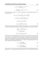
MOSFET-like CNTFET
First, we present a compact model for CNTFETs with a classical behavior.
This compact model is based on a CNTFET model developed at Purdue University [5]. To our best knowledge, Purdue’s model is the first compact model (i.e.
fully dedicated to circuit simulation) of CNTFET available in the literature. It
is a surface potential-based SPICE compatible model that enables to simulate
CNTs with ballistic behavior. It has been incorporated in HSPICE but is not
well-suited for circuit simulation due to some convergence issues.
In this paper, we propose a modified model with fundamental improvements
solving the convergence problems of the original model. The new model is
applicable to a wide range of CNTFETs with diameters between 1 and 3 nm
and for all chiralities as long as they are semiconducting. The model uses
suitable approximations necessary for developing any quasi-analytical, circuitcompatible compact model (see Fig. 1.5). Quasi-static characteristics (I–V )
have been modeled and validated against numerical models, with an excellent
agreement.
The computional procedure to evaluate the drain current ID and the total
channel charge QCN T is illustrated in Fig. 1.6. The main quantities used in the
model are the surface potential ψS (or control potential) and the specific voltage
ξS(D) that depends on the surface potential, the subbands energy level ∆p and
the source (drain) Fermi level µS(D) . The conduction band minima for the first
subband is set to half the nanotube bandgap ∆1 with ∆1 0.45/diam (in eV).
Drain
CGD
RD
Gate
ID
VFB
CGS
CGD
CGS
RD
RS
VFB
ID
gate-drain capacitance
gate-source capacitance
drain resistance
source resistance
flatband voltage
drain current
RS
Source
Figure 1.5.
Schematic of the CNTFET compact model.
Compact Modeling of Emerging Technologies with VHDL-AMS
13
diam, VFB, TYP, p (only for test purpose)
Precomputed
parameters: α, ∆VFB
VG, VD, VS
Subband minima ∆p
Control potential: ψS
Source/Drain Fermi
level: µS, µD
Specific voltage: ξS, ξD
ξS/D = (ψS-∆p-µS/D)/(kB.T)
Drain current: ID
Figure 1.6.
Channel charge: QCNT
Capacitances: CGS, CGD
Structure of the CNTFET compact model.
The physical parameter diam is the nanotube diameter (in nm); it is one of the
only three intrinsic parameters of our model, with the flatband voltage VF B and
the TYP parameter (= +1/ − 1 for n- or p-type device). Let us emphasize
the number of subbands p has been added as an input parameter only for test
purpose [16].
Determination of the surface potential.
An important step in the model
development is to relate the control potential with the gate bias voltage (see
Fig. 1.6). The knowledge of ψS is useful to calculate the specific voltage ξ.
This allows us to determine the drain current and the total charge. In [5], the
following approximation has been proposed
VGS − ψS =
0
for VGS < ∆1 ,
α · (VGS − ∆1 ) for VGS ∆1 .
(1.5)
where the parameter α is given by
2
α = α0 + α1 · VDS + α2 · VDS
(1.6)
where α0 , α1 , and α2 are dependent on both CNTFET diameter and gate
oxide thickness [16]. Eq. (1.5) is correct to model the relationship between
the gate voltage and the surface potential, but is not well-suited for a compact
model (problem of discontinuity, as shown in Fig. 1.7). Therefore, we propose
14
ADVANCES IN DESIGN AND SPECIFICATION OF EMBEDDED SYSTEMS
1.1
VDS = 0V
VDS = 0.5V
VDS = 0V
VDS = 0.5V
dψS/dVGS
1.0
[5]
[5]
[Our model]
[Our model]
0.9
0.8
0.7
0.12
0.13
0.14
0.15
0.16
0.17
0.18
Gate voltage, VGS (V)
Figure 1.7.
Derivative of surface potential ψS vs. VGS .
an equivalent solution, given by (1.7), but with an excellent behavior of the
derivative (see Fig. 1.7)
ψS = VGS −
α(VGS − ∆1 ) +
[α(VGS − ∆1 )]2 + 4
2
2
(1.7)
where = 5 · 10−2 is a smoothing parameter.
Then, the total drain current ID is obtained as
ID =
4 q kB T
h
[ln (1 + exp(ξS )) − ln (1 + exp(ξD ))]
(1.8)
p
where p is the number of subbands, kB and h are the constants of Boltzmann
and Planck, respectively.
Quantum-Capacitance Derivation.
With the knowledge of charge and
surface potential as functions of gate bias, the gate input capacitance CG can
be computed in terms of the device parameters and terminal voltages. The gate
input capacitance is given by
CG =
∂QCN T
∂VGS
⇒ CG =
∂QCN T ∂ψS
·
∂ψS
∂VGS
(1.9)
The total charge QCN T can be split up into QS and QD and, hence, the total
gate capacitance can also be split up into CGS and CGD (see Fig. 1.5).
To elaborate an efficient expression of CG for a compact model, it is important
to first have a closed-form expression of QCN T (ψS ) and continuous derivatives
of (1.9) as well. As it is not possible to obtain a closed-form relationship for the
15
Compact Modeling of Emerging Technologies with VHDL-AMS
quantum-charge in the channel, an empirical solution (fit) has been proposed in
[5]. Noting that the number of carrier n increases almost linearly as ξ increases
and falls off exponentially as ξ becomes negative, the following relationship
has been derived
n=
for ξ < 0,
N0 · A · exp ξ
N0 · (B · ξ + A) for ξ 0.
(1.10)
where the parameters A and B are dependent on the energy level ∆ [5].
Eq. (1.10) is unfortunately not appropriate for circuit simulation because
its derivatives are not continuous (Fig. 1.8). Accordingly, the different capacitances determined by (1.10) would not be correct to elaborate the CNTFET
dynamic model. In addition, this would lead to numerical problems during simulation and wrong results. In order to solve the numerical problems, we have
elaborated a new equation for n, similar to the interpolation function of the
EKV MOSFET model [10]. This new expression and its derivatives (Fig. 1.8)
are continuous and well-suited for circuit simulation, especially in dynamic
operation
nnew (ξ) = N0 · 1.2 · B · ln 1 +
A
· exp
1.2 · B
ξ
0.96
0.96
(1.11)
Figure 1.8 shows a comparison between the derivatives of (1.10) and (1.11).
Let us note that the greatest difference can be observed around zero, where
actually the former overestimates the quantum-charge (see Fig. 4 in [5]). The
VHDL-AMS simulation of the capacitances computed with our continuous
model is shown in Fig. 1.9.
Figure 1.10 shows the drain current of a 1.4 nm diameter CNTFET with
Cox = 3.8 pF/cm as a function of gate voltage. The dots correspond to the
4
∆
∆
∆
∆
d(n/N0)/dξ
3
= 0.15 eV [5]
= 0.35 eV [5]
= 0.15 eV [this work]
= 0.35 eV [this work]
2
1
0
−4
Figure 1.8.
−2
0
ξ
2
4
Improvement of the numerical behavior.
16
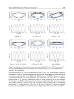
ADVANCES IN DESIGN AND SPECIFICATION OF EMBEDDED SYSTEMS
Normalized capacitances (-)
0.25
0.20
VDS = 0.1 V
d = 1.4 nm
TYP = 1
p=1
VFB = 0
Rseries = 0
0.15
0.10
CGS /Cox
CGD /Cox
0.05
0.0
0.2
0.4
0.6
Gate voltage, VGS (V)
0.8
1.0
Figure 1.9. VHDL-AMS simulation of the CGS and CGD capacitances for a MOSFET-like
CNTFET with Cox = 3.8 pF/cm.
100
100
80
3
2
60
10
7
6
5
4
40
VDS = 40 mV
VDS = 1 V
3
2
1
0.0
0.1
0.2
0.3
0.4
0.5
0.6
0.7
ID (µA) in linear scale
ID (µA) in log. scale
7
6
5
4
20
0.8
Gate voltage, VGS (V)
Figure 1.10. Comparison between the results extracted from VHDL-AMS and numerical simulations (lines and dots, respectively) for the drain current of a MOSFET-like CNTFET (p = 1,
diam = 1.4, TYP = +1, VFB = 0, Rseries = 0).
numerical solutions performed with the FETToy simulator [17] whereas the
lines correspond to our analytical compact model. A good agreement is found,
which supports the validity of our approach.
VHDL-AMS Implementation
First, we have calibrated the model of Purdue with respect to numerical
simulations [18, 17]. The best fits were obtained with p = 1 (i.e. one subband)
17
Compact Modeling of Emerging Technologies with VHDL-AMS
which is coherent because the FETToy simulator only accounts for the lowest
subband. So, at the beginning, we fixed p = 1 in our model in order to validate
it with respect to the numerical simulations. Then, if we consider CNTFETs
with diameters ranging from 1 to 3 nm, and with a power supply lower than
1 V, we can set p = 5 to accurately describe all cases [16].
The whole VHDL-AMS code of the model requires about 90 lines. Only
three intrinsic parameters are necessary: diam, TYP (+1 for n-type, −1 for
p-type) and VF B (lines 5–7 in Listing 2).
(1)
(2)
(3)
(4)
(5)
(6)
(7)
(8)
(9)
(10)
(11)
library ieee; library disciplines;
use disciplines.electromagnetic_system.all;
use work.all;
entity CNTFET is
generic(diam
: real := 1.4; -- Nanotube diameter [nm]
TYP
: real := 1.0; -- n/p-CNTFET (+1/-1)
VFB
: real := 0.0; -- Flatband voltage [V]
p
: positive := 1; -- Number of subbands [-]
Rseries : real := 50.0e3); -- Series resistance [ohm]
port(terminal g,d,s : electrical);
end;
Listing 2. Interface of the CNTFET VHDL-AMS model: the entity.
Let us note that the number of subbands p has been defined as a generic
parameter only for test purpose [16]. Rseries corresponds to the total series
resitance, that is Rsource +Rdrain with Rsource = Rdrain . The parameters α0 , α1 ,
and α2 [see (1.6)] are determined in a precomputed module, with the help of
one equation for each of them. For all details about the computation of the
parameters α, the reader is referred to [16].
To conclude this section, Fig. 1.11 shows two VHDL-AMS simulations performed for different values of the parameters diam and p, in order to show the
effect of the nanotube diameter on the number of subbands p to be accounted for.
This behavior may be useful to create novel multiple-valued logic design [19].
4.0
6
Diameter = 1 nm
Cox = 3.8 pF/cm
VDS = 20 mV
Diameter = 2 nm
Cox = 3.8 pF/cm
VDS = 20 mV
5
3.0
ID (µA)
ID (µA)
3.5
2.5
4
3
p=1
p=2
2.0
1.5
0.0
0.1
0.2
0.3
0.4
0.5
0.6
Gate voltage, VGS (V)
Figure 1.11.
0.7
p=1
p=2
2
0.8
0.0
0.1
0.2
0.3
0.4
0.5
0.6
0.7
Gate voltage, VGS (V)
VHDL-AMS simulations of ID vs. VGS at low drain bias.
0.8
18
ADVANCES IN DESIGN AND SPECIFICATION OF EMBEDDED SYSTEMS
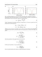
Ambipolar CNTFET
We present, for the first time to our best knowledge, a behavioral compact
model that allows to describe the ambipolar characteristic of SB CNTFETs.
This model is built using the new model of CNTFET previously presented. As
shown in Fig. 1.12, an additional part has been added to the “unipolar” model.
The entity (VHDL-AMS) corresponding to this new model is the same as the
classical CNTFET model one.
The very particular ID –VGS characteristic of the ambipolar CNTFET is
illustrated in Fig. 1.13. It should be noted that this behavior is quite similar to the numerical simulation results recently published in [20] and [21]. This
Unipolar CNTFET model (e.g., n-type)
Input voltage: VGS
VGS_EFF = −VGS + VDS
ID_n
pseudo ID_p
+
Ambipolar drain current model: ID
Figure 1.12.
Structure of the behavioral model for the ambipolar CNTFET.
10−4
ID (A)
10−5
10−6
10−7
10−8
−0.8
VDS = 0.2V
VDS = 0.4V
VDS = 0.6V
VDS = 0.8V
−0.6
−0.4
−0.2
0.0
0.2
0.4
0.6
Gate voltage, VGS (V)
Figure 1.13. VHDL-AMS simulation of the drain current as a function of gate voltage for the
ambipolar SB CNTFET (p = 1, diam = 1.4, TYP = +1, VFB = 0, Rseries = 0).