Tài liệu Verilog Examples part 2 doc
Bạn đang xem bản rút gọn của tài liệu. Xem và tải ngay bản đầy đủ của tài liệu tại đây (15.16 KB, 5 trang )
[ Team LiB ]
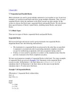
F.2 Behavioral DRAM Model
This example describes a behavioral implementation of a 256K x 16 DRAM. The DRAM
has 256K 16-bit memory locations. The input/output ports of the DRAM are shown in
Figure F-2
.
Figure F-2. DRAM Input/Output Ports
Input ports
All ports with a suffix "N" are low-asserted.
MA— 10-bit memory address
OE_N— Output enable for reading data
RAS_N— Row address strobe for asserting row address
CAS_N— Column address strobe for asserting column address
LWE_N— Lower write enable to write lower 8 bits of DATA into memory
UWE_N— Upper write enable to write upper 8 bits of DATA into memory
Inout ports
DATA— 16-bit data as input or output. Write input if LWE_N
or UWE_N is asserted. Read output if OE_N is asserted.
The Verilog HDL code for the DRAM implementation is shown in Example F-2.
Example F-2 Behavioral DRAM Model
////////////////////////////////////////////////////////////////////
// FileName: "dram.v" - functional model of a 256K x 16 DRAM
// Author : Venkata Ramana Kalapatapu
// Company : Sand Microelectronics Inc.(now a part of Synopsys, Inc.)
// Profile : Sand develops Simulation Models, Synthesizable Cores, and
// Performance Analysis Tools for Processors, buses and
// memory products. Sand's products include models for
// industry-standard components and custom-developed
// models for specific simulation environments.
//
////////////////////////////////////////////////////////////////////
module DRAM( DATA,
MA,
RAS_N,
CAS_N,
LWE_N,
UWE_N,
OE_N);
inout [15:0] DATA;
input [9:0] MA;
input RAS_N;
input CAS_N;
input LWE_N;
input UWE_N;
input OE_N;
reg [15:0] memblk [0:262143]; // Memory Block. 256K x 16.
reg [9:0] rowadd; // RowAddress Upper 10 bits of MA.
reg [7:0] coladd; // ColAddress Lower 8 bits of MA.
reg [15:0] rd_data; // Read Data.
reg [15:0] temp_reg;
reg hidden_ref;
reg last_lwe;
reg last_uwe;
reg cas_bef_ras_ref;
reg end_cas_bef_ras_ref;
reg last_cas;
reg read;
reg rmw;
reg output_disable_check;
integer page_mode;
assign #5 DATA=(OE_N===1'b0 && CAS_N===1'b0) ? rd_data : 16'bz;
parameter infile = "ini_file"; // Input file for preloading the Dram.
initial
begin
$readmemh(infile, memblk);
end
always @(RAS_N)
begin
if(RAS_N == 1'b0 ) begin
if(CAS_N == 1'b1 ) begin
rowadd = MA;
end
else
hidden_ref = 1'b1;
end
else
hidden_ref = 1'b0;
end
always @(CAS_N)
#1 last_cas = CAS_N;
always @(CAS_N or LWE_N or UWE_N)
begin
if(RAS_N===1'b0 && CAS_N===1'b0 ) begin
if(last_cas==1'b1)
coladd = MA[7:0];
if(LWE_N!==1'b0 && UWE_N!==1'b0) begin // Read Cycle.
rd_data = memblk[{rowadd, coladd}];
$display("READ : address = %b, Data = %b",
{rowadd,coladd}, rd_data );
end
else if(LWE_N===1'b0 && UWE_N===1'b0) begin
// Write Cycle both bytes.
memblk[{rowadd,coladd}] = DATA;
$display("WRITE: address = %b, Data = %b",
{rowadd,coladd}, DATA );
end
else if(LWE_N===1'b0 && UWE_N===1'b1) begin
// Lower Byte Write Cycle.
temp_reg = memblk[{rowadd, coladd}];
temp_reg[7:0] = DATA[7:0];
memblk[{rowadd,coladd}] = temp_reg;
end
else if(LWE_N===1'b1 && UWE_N===1'b0) begin
// Upper Byte Write Cycle.
temp_reg = memblk[{rowadd, coladd}];
temp_reg[15:8] = DATA[15:8];
memblk[{rowadd,coladd}] = temp_reg;
end
end
end
// Refresh.
always @(CAS_N or RAS_N)
begin
if(CAS_N==1'b0 && last_cas===1'b1 && RAS_N===1'b1) begin
cas_bef_ras_ref = 1'b1;
end
if(CAS_N===1'b1 && RAS_N===1'b1 && cas_bef_ras_ref==1'b1) begin
end_cas_bef_ras_ref = 1'b1;
cas_bef_ras_ref = 1'b0;
end
if( (CAS_N===1'b0 && RAS_N===1'b0) && end_cas_bef_ras_ref==1'b1 )
end_cas_bef_ras_ref = 1'b0;
end
endmodule
[ Team LiB ]