dye, n. (2000). radio frequency transistors - principles and practical applicat
Bạn đang xem bản rút gọn của tài liệu. Xem và tải ngay bản đầy đủ của tài liệu tại đây (7.3 MB, 317 trang )
1
2
3
4
5
6
7
8
9
10
11
12
13
14
15
16
17
18
19
20
21
22
23
24
25
26
27
28
29
30
31
32
33
34
35
36
37
38
39
40
41
42
43
44
45Short
46Reg
Radio
Frequency
Transistors
10500_00_i-xvi_7jb.qxd 11/20/00 2:55 PM Page i
1
2
3
4
5
6
7
8
9
10
11
12
13
14
15
16
17
18
19
20
21
22
23
24
25
26
27
28
29
30
31
32
33
34
35
36
37
38
39
40
41
42
43
44
Short45
Reg46
10500_00_i-xvi_7jb.qxd 11/20/00 2:55 PM Page ii
Radio
Frequency
Transistors
Principles and Practical Applications
Second Edition
Norman Dye
Helge Granberg
Boston Oxford Johannesburg Melbourne New Delhi
1
2
3
4
5
6
7
8
9
10
11
12
13
14
15
16
17
18
19
20
21
22
23
24
25
26
27
28
29
30
31
32
33
34
35
36
37
38
39
40
41
42
43
44
45Short
46Reg
10500_00_i-xvi_7jb.qxd 11/20/00 2:55 PM Page iii
Newnes is an imprint of Butterworth–Heinemann.
Copyright © 2001 by Butterworth–Heinemann
A member of the Reed Elsevier group
All rights reserved.
No part of this publication may be reproduced, stored in a retrieval system, or transmitted in
any form or by any means, electronic, mechanical, photocopying, recording, or otherwise,
without the prior written permission of the publisher.
Recognizing the importance of preserving what has been written, Butterworth–
Heinemann prints its books on acid-free paper whenever possible.
Butterworth–Heinemann supports the efforts of American Forests and the Global
ReLeaf program in its campaign for the betterment of trees, forests, and our
environment.
Library of Congress Cataloging-in-Publication Data
Dye, Norm, 1929–
Radio frequency transistors : principles and practical
applications / Norman Dye, Helge Granberg.—2nd ed.
p. cm.
Includes bibliographical references and index.
ISBN 0-7506-7281-1 (pbk. : alk. paper)
1. Power transistors. 2. Transistor amplifiers. 3. Transistor
radio transmitters. 4. Amplifiers, Radio frequency. I. Granberg,
Helge, 1932– II. Title.
TK7871.92 .D96 2000
621.384'12—dc21 00-045618
British Library Cataloguing-in-Publication Data
A catalogue record for this book is available from the British Library.
The publisher offers special discounts on bulk orders of this book.
For information, please contact:
Manager of Special Sales
Butterworth-Heinemann
225 Wildwood Avenue
Woburn, MA 01801-2041
Tel: 781-904-2500
Fax: 781-904-2620
For information on all Newnes publications available, contact our World Wide Web home
page at:
10987654321
Printed in the United States of America
1
2
3
4
5
6
7
8
9
10
11
12
13
14
15
16
17
18
19
20
21
22
23
24
25
26
27
28
29
30
31
32
33
34
35
36
37
38
39
40
41
42
43
44
Short45
Reg46
10500_00_i-xvi_7jb.qxd 11/20/00 2:55 PM Page iv
Dedicated to the memory of Helge Granberg,
who died suddenly in January, 1996
1
2
3
4
5
6
7
8
9
10
11
12
13
14
15
16
17
18
19
20
21
22
23
24
25
26
27
28
29
30
31
32
33
34
35
36
37
38
39
40
41
42
43
44
45Short
46Reg
10500_00_i-xvi_7jb.qxd 11/20/00 2:55 PM Page v
1
2
3
4
5
6
7
8
9
10
11
12
13
14
15
16
17
18
19
20
21
22
23
24
25
26
27
28
29
30
31
32
33
34
35
36
37
38
39
40
41
42
43
44
Short45
Reg46
10500_00_i-xvi_7jb.qxd 11/20/00 2:55 PM Page vi
CONTENTS
Preface xi
Acknowledgments xiii
CHAPTER 1 Understanding RF Data Sheet Parameters 1
Introduction 1
D.C. Specifications 1
Maximum Ratings and Thermal Characteristics 5
Power Transistors: Functional Characteristics 9
Low Power Transistors: Functional Characteristics 14
Linear Modules: Functional Characteristics 18
Power Modules: Functional Characteristics 26
Data Sheets of the Future 30
CHAPTER 2 RF Transistor Fundamentals 31
What’s Different About RF Transistors? 31
Transistor Characteristics in Specific Applications 32
Bandwidth Considerations in Selecting Transistors 34
MOSFETs Versus Bipolars in Selecting a Transistor 38
Other Factors in RF Power Transistor Selection 38
CHAPTER 3 FETs and BJTs: Comparison of Parameters
and Circuitry
43
Types of Transistors 43
Comparing the Parameters 44
Circuit Configurations 48
Common Emitter and Common Source 50
Common Base and Common Gate 52
Common Collector and Common Drain 54
CHAPTER 4 Other Factors Affecting Amplifier Design 57
Classes of Operation 57
Forms of Modulation 60
Biasing to Linear Operation 64
Operating Transistors in a Pulse Mode 72
CHAPTER 5 Reliability Considerations 75
Die Temperature and Its Effect on Reliability 75
Other Reliability Considerations 81
CHAPTER 6 Construction Techniques 87
Types of Packages 87
The Emitter/Source Inductance 93
Laying Out a Circuit Board 97
1
2
3
4
5
6
7
8
9
10
11
12
13
14
15
16
17
18
19
20
21
22
23
24
25
26
27
28
29
30
31
32
33
34
35
36
37
38
39
40
41
42
43
44
45Short
46Reg
10500_00_i-xvi_7jb.qxd 11/20/00 2:55 PM Page vii
Tips for Systematic PC Layout Design 102
Mounting RF Devices 103
RF Modules 109
CHAPTER 7 Power Amplifier Design 113
Single-Ended, Parallel, or Push-Pull 113
Single-Ended RF Amplifier Designs: Lumped Circuit Realization 113
Distributed Circuit Realization 114
Quasi-Lumped Element Realization 116
Parallel Transistor Amplifiers: Bipolar Transistors 117
MOSFETs 119
Push-Pull Amplifiers 120
Impedances and Matching Networks 123
Interstage Impedance Matching 127
A Practical Design Example of a Single Stage 129
Component Considerations 130
Capacitors at Radio Frequencies 132
The First Matching Element: A Shunt C 133
The Input Impedance of a High Power RF Transistor 134
Modeling Capacitors at Low Impedances 135
Inductors 136
Stability Considerations 137
CHAPTER 8 Computer-Aided Design Programs 147
General 147
Inside Motorola’s Impedance Matching Program 151
MIMP Description 154
Smith Charts and MIMP 157
CHAPTER 9 After the Power Amplifier 161
VSWR Protection of Solid State Amplifiers 161
Testing the Circuit 165
Output Filtering 168
Types of Low Pass Filters 170
The Design Procedure 172
The Components 174
CHAPTER 10 Wideband Impedance Matching 179
Introduction to Wideband Circuits 179
Conventional Transformers 182
Twisted Wire Transformers 186
Transmission Line Transformers 190
Equal Delay Transmission Line Transformers 193
viii Contents
1
2
3
4
5
6
7
8
9
10
11
12
13
14
15
16
17
18
19
20
21
22
23
24
25
26
27
28
29
30
31
32
33
34
35
36
37
38
39
40
41
42
43
44
Short45
Reg46
10500_00_i-xvi_7jb.qxd 11/20/00 2:55 PM Page viii
CHAPTER 11 Power Splitting and Combining 197
Introduction 197
Basic Types of Power Combiners 198
In-Phase and 180° Combiners 199
90° Hybrids 202
Line Hybrids 203
Ring Hybrids 204
Branch Line Couplers 206
Wilkinson Couplers 208
CHAPTER 12 Frequency Compensation and
Negative Feedback
211
Frequency Compensation 211
Negative Feedback 213
CHAPTER 13 Small Signal Amplifier Design 219
Scattering Parameters 219
Noise Parameters 220
Biasing Considerations 221
Power Gain 224
Stability 229
Summary of Gain/Noise Figure Design Procedures 233
Actual Steps in Low Power Amplifier Design 234
Determining Desired Values of Source and Load Impedances 235
Circuit Realization 243
CHAPTER 14 LDMOS RF Power Transistors and
Their Applications
259
by Prasanth Perugupalli, Larry Leighton, Jan Johansson,
and Qiang Chen
Introduction 259
LDMOSFET Versus Vertical MOSFET 260
Device Design 261
LDMOS Characteristics 264
LDMOS Transistors for RF Power Applications 267
Some FET Approximations 267
Applications of LDMOS Transistors in Current Generation
Cellular Technologies 271
RF Power Amplifier Characteristics 273
Practical Example of Designing a W-CDMA Power Amplifier 277
Circuit Techniques for Designing Optimum CDMA Amplifiers 281
Modeling of LDMOS Transistors 283
Comments 290
Index 293
Contents ix
1
2
3
4
5
6
7
8
9
10
11
12
13
14
15
16
17
18
19
20
21
22
23
24
25
26
27
28
29
30
31
32
33
34
35
36
37
38
39
40
41
42
43
44
45Short
46Reg
10500_00_i-xvi_7jb.qxd 11/20/00 2:55 PM Page ix
1
2
3
4
5
6
7
8
9
10
11
12
13
14
15
16
17
18
19
20
21
22
23
24
25
26
27
28
29
30
31
32
33
34
35
36
37
38
39
40
41
42
43
44
Short45
Reg46
10500_00_i-xvi_7jb.qxd 11/20/00 2:55 PM Page x
PREFACE
This book is about radio frequency (RF) transistors. It primarily focuses on ap-
plications viewed from the perspective of a semiconductor supplier who, over the
years, has been involved not only in the manufacture of RF transistors, but also
their use in receivers, transmitters, plasma generators, magnetic resonance imag-
ing, etc.
Since the late 1960s, Motorola Semiconductors has been at the forefront in the
development of solid state transistors for use at radio frequencies. The authors
have been a part of this development since 1970. Much information has been ac-
quired during this time, and it is our intention in writing this book to make the
bulk of that information available to users of RF transistors in a concise manner
and from a single source.
This book is not theoretical; as the name implies, it is intended to be practical.
Some mathematics is encountered during the course of the book, but it is not rig-
orous. Formulas are not derived; however, sufficient references are cited for the
reader who wishes to delve deeper into a particular subject.
This book is slanted toward power transistors and their applications because
much less material is available in the literature on this subject, particularly in one
location. Also, RF power is the primary experience of the authors. One chapter is
devoted to low power (small signal) transistor applications in an effort to cover
more completely the breadth of power levels in RF transistors.
Chapters 1 through 4 discuss RF transistor fundamentals, such as what’s dif-
ferent about RF transistors, how they are specified, how to select a transistor, and
what the difference is between FETs and BJTs. Also covered are topics such as
classes of operation, forms of modulation, biasing, and operating in a pulse
mode. Chapters 5 and 6 lay the groundwork for future circuit designs by dis-
cussing such subjects as laying out circuit boards and mounting RF devices, as
well as the importance of die temperature.
In Chapters 7, 8, and 9, the authors take the reader through various considera-
tions in planning an amplifier design. Among the diverse topics covered are
choice of circuit, stability, impedance matching (including computer-aided de-
1
2
3
4
5
6
7
8
9
10
11
12
13
14
15
16
17
18
19
20
21
22
23
24
25
26
27
28
29
30
31
32
33
34
35
36
37
38
39
40
41
42
43
44
45Short
46Reg
10500_00_i-xvi_7jb.qxd 11/20/00 2:55 PM Page xi
sign programs), and the power amplifier output. Chapters 10 through 12 focus on
wideband techniques.
Chapter 13 describes the many factors affecting small signal (low power) am-
plifier design. A variety of examples illustrate the concepts in an effort to make
small signal amplifier design straightforward through a step-by-step approach.
About the Revision
The second edition of the book is being issued primarily to provide updated in-
formation on the newest transistor type to arrive on the RF power scene, namely
LDMOS FETs. An entire chapter (Chapter 14) is devoted to this subject and
takes the reader from die design, through modulation requirements of today’s
cellular radios, to the actual design of a high power amplifier using LDMOS
FETs.
In addition, material has been added in Chapter 2 regarding selection of
matched transistors, and in Chapter 7, a significant amount of material has been
added on capacitors, inductors, and impedance matching. Finally, an example of
the use of S-parameters in the design of a low power, low noise amplifier has
been added at the end of Chapter 13.
xii Preface
1
2
3
4
5
6
7
8
9
10
11
12
13
14
15
16
17
18
19
20
21
22
23
24
25
26
27
28
29
30
31
32
33
34
35
36
37
38
39
40
41
42
43
44
Short45
Reg46
10500_00_i-xvi_7jb.qxd 11/20/00 2:55 PM Page xii
ACKNOWLEDGMENTS
The authors wish to thank the many application engineers in the RF product op-
eration at Motorola Semiconductors for their contributions to the book. Special
recognition goes to Phuong Le for his assistance in low power applications, to
Dan Moline for making available his recently introduced computer program for
impedance matching with the aid of Smith Chart™ displays, to Bob Baeten for
his assistance in computer-aided design programs, to Walt Wright for answering
many questions about microwaves and pulse power applications, and to Hank
Pfizenmayer for his advice and expertise in filter design. Special thanks also go
to Analog Instruments Co., Box 808, New Providence, NJ 07974, for their per-
mission to reproduce the Smith Chart in several diagrams in Chapter 13. And
special thanks go to the management of the Communications Semiconductor
Products Division within Motorola Semiconductor Sector, whose encouragement
and support has made writing this book possible.
Both authors retired from Motorola Semiconductors in 1994. In order to give
the reader the latest and best possible information about LDMOS transistors,
Norm Dye enlisted, through the courtesy of Tom Moller, Vice President and
General Manager of Ericsson, Inc., Microelectronics Division, the aid of the staff
at Ericsson RF Power Products, Microelectronics Division to revise this book.
Thus, Chapter 14 has been written primarily by Prasanth Perugupalli from the
Ericsson Phoenix Design Center in Scottsdale, Arizona. Some of the material on
LDMOS die was contributed by Jon Johansson, and information on die modeling
was contributed by Qiang Chen, both located in Ericsson’s transistor manufactur-
ing facility in Stockholm, Sweden.
Some of the material on applications has also been contributed by Larry
Leighton, manager of the Phoenix Design Center. Finally, comments and review
of the technical material have been made by Nagaraj Dixit, also of the Ericsson
Phoenix Design Center team. Special thanks to each of these gentlemen for their
assistance, without which this second edition would not be possible.
1
2
3
4
5
6
7
8
9
10
11
12
13
14
15
16
17
18
19
20
21
22
23
24
25
26
27
28
29
30
31
32
33
34
35
36
37
38
39
40
41
42
43
44
45Short
46Reg
Smith Chart™ is a registered trademark of Analog Instruments.
10500_00_i-xvi_7jb.qxd 11/20/00 2:55 PM Page xiii
1
2
3
4
5
6
7
8
9
10
11
12
13
14
15
16
17
18
19
20
21
22
23
24
25
26
27
28
29
30
31
32
33
34
35
36
37
38
39
40
41
42
43
44
Short45
Reg46
10500_00_i-xvi_7jb.qxd 11/20/00 2:55 PM Page xiv
1
2
3
4
5
6
7
8
9
10
11
12
13
14
15
16
17
18
19
20
21
22
23
24
25
26
27
28
29
30
31
32
33
34
35
36
37
38
39
40
41
42
43
44
45Short
46Reg
Radio
Frequency
Transistors
10500_00_i-xvi_7jb.qxd 11/20/00 2:55 PM Page xv
1
2
3
4
5
6
7
8
9
10
11
12
13
14
15
16
17
18
19
20
21
22
23
24
25
26
27
28
29
30
31
32
33
34
35
36
37
38
39
40
41
42
43
44
Short45
Reg46
10500_00_i-xvi_7jb.qxd 11/20/00 2:55 PM Page xvi
1
2
3
4
5
6
7
8
9
10
11
12
13
14
15
16
17
18
19
20
21
22
23
24
25
26
27
28
29
30
31
32
33
34
35
36
37
38
39
40
41
42
43
44
45Short
46Reg
1
Understanding
RF Data Sheet Parameters
INTRODUCTION
Data sheets are often the sole source of information about the capability and
characteristics of a product. This is particularly true of unique RF semiconductor
devices that are used by equipment designers all over the world. Because circuit
designers often cannot talk directly with the factory, they rely on the data sheet
for their device information.
1
And for RF devices, many of the specifications are
unique in themselves. Thus it is important that the user and the manufacturer of
RF products speak a common language—that is, what semiconductor manufactur-
ers say about their RF devices should be understood fully by the circuit designers.
In this chapter, a review is given of RF transistor and amplifier module param-
eters from maximum ratings to functional characteristics. The section is di-
vided into five basic parts: D.C. specifications, power transistors, low power
transistors, power modules, and linear modules. Comments are made about criti-
cal specifications, about how values are determined and what their significance
is. A brief description of the procedures used to obtain impedance data and ther-
mal data is set forth, the importance of test circuits is elaborated, and background
information is given to help understand low noise considerations and linearity re-
quirements.
D.C. SPECIFICATIONS
Basically, RF transistors are characterized by two types of parameters: D.C. and
functional. The “D.C.” specs consist (by definition) of breakdown voltages, leak-
age currents, h
FE
(D.C. beta), and capacitances, while the functional specs cover
gain, ruggedness, noise figure, Z
in
and Z
out
, S-parameters, distortion, etc. Ther-
mal characteristics do not fall cleanly into either category since thermal resis-
tance and power dissipation can be either D.C. or A.C. Thus, we will treat the
spec of thermal resistance as a special specification and give it its own heading
called “thermal characteristics.” Figure 1-1 is one page of a typical RF power
data sheet showing D.C. and functional specs.
A critical part of selecting a transistor is choosing one that has breakdown
voltages compatible with the supply voltage available in an intended application.
10500_01_001-030_R3_jb.qxd 11/20/00 3:07 PM Page 1
2 Radio Frequency Transistors
1
2
3
4
5
6
7
8
9
10
11
12
13
14
15
16
17
18
19
20
21
22
23
24
25
26
27
28
29
30
31
32
33
34
35
36
37
38
39
40
41
42
43
44
Short45
Reg46
FIGURE 1-1
Typical D.C. and functional specifications from a RF power data sheet. The references in the “Notes”
above to a test fixture and “Figure 1” pertain to the data sheet from which this figure was extracted.
It is important that the design engineer select a transistor on the one hand that
has breakdown voltages which will not be exceeded by the D.C. and RF voltages
that appear across the various junctions of the transistor and on the other hand
has breakdown voltages that permit the “gain at frequency” objectives to be met
by the transistor.
Mobile radios normally operate from a 12-volt source, and portable radios use
a lower voltage, typically 6 to 9 volts. Avionics applications are commonly 28-
volt supplies, while base station and other ground applications such as medical
electronics generally take advantage of the superior performance characteristics
of high-voltage devices and operate with 24- to 50-volt supplies. In making a
transistor, breakdown voltages are largely determined by material resistivity and
junction depths (see Figure 1-2).
2
It is for these reasons that breakdown voltages
are intimately entwined with functional performance characteristics. Most prod-
uct portfolios in the RF power transistor industry have families of transistors de-
10500_01_001-030_R3_jb.qxd 11/20/00 3:07 PM Page 2
Understanding RF Data Sheet Parameters 3
1
2
3
4
5
6
7
8
9
10
11
12
13
14
15
16
17
18
19
20
21
22
23
24
25
26
27
28
29
30
31
32
33
34
35
36
37
38
39
40
41
42
43
44
45Short
46Reg
FIGURE 1-2
The effect of curvature and resistivity on breakdown voltage.
signed for use at specified supply voltages such as 7.5 volts, 12.5 volts, 28 volts,
and 50 volts.
Leakage currents (defined as reverse biased junction currents that occur prior
to avalanche breakdown) are likely to be more varied in their specification, and
also more informative. Many transistors do not have leakage currents specified
because they can result in excessive (and frequently unnecessary) wafer/die yield
losses. Leakage currents arise as a result of material defects, mask imperfections,
and/or undesired impurities that enter during wafer processing. Some sources of
leakage currents are potential reliability problems; most are not. Leakage cur-
rents can be material-related, such as stacking faults and dislocations, or they
can be “pipes” created by mask defects and/or processing inadequacies. These
sources result in leakage currents that are constant with time, and if initially ac-
ceptable for a particular application, will remain so. They do not pose long-term
reliability problems.
On the other hand, leakage currents created by channels induced by mobile ionic
contaminants in the oxide (primarily sodium) tend to change with time and can lead
to increases in leakage current that render the device useless for a specific applica-
tion. Distinguishing between sources of leakage current can be difficult, which is
one reason devices for application in military environments require HTRB (high
temperature reverse bias) and burn-in testing. However, even for commercial appli-
cations—particularly where battery drain is critical or where bias considerations
dictate limitations—it is essential that a leakage current limit be included in any
complete device specification.
10500_01_001-030_R3_jb.qxd 11/20/00 3:07 PM Page 3
4 Radio Frequency Transistors
1
2
3
4
5
6
7
8
9
10
11
12
13
14
15
16
17
18
19
20
21
22
23
24
25
26
27
28
29
30
31
32
33
34
35
36
37
38
39
40
41
42
43
44
Short45
Reg46
FIGURE 1-3
Relationship between transistor beta and operating frequency.
D.C. parameters such as h
FE
and C
ob
(output capacitance) need little comment.
Typically, for RF devices, h
FE
is relatively unimportant for unbiased power transis-
tors because the functional parameter of gain at the desired frequency of operation
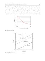
is specified. Note, though, that D.C. beta is related to A.C. beta (see Figure 1-3).
Functional gain will track D.C. beta, particularly at lower RF frequencies. An h
FE
specification is needed for transistors that require bias, which includes most small
signal devices that are normally operated in a linear (Class A) mode (see Chapter 4,
“Other Factors Affecting Amplifier Design”). Generally, RF device manufacturers
do not like to have tight limits placed on h
FE
. The primary reasons that justify this
position are:
a. Lack of correlation with RF performance
b. Difficulty in control in wafer processing
c. Other device manufacturing constraints dictated by functional perfor-
mance specs (which preclude tight limits for h
FE
)
A good rule of thumb for h
FE
is to set a maximum-to-minimum ratio of not
less than 3 and not more than 4, with the minimum h
FE
value determined by an
acceptable margin in functional gain.
Output capacitance is an excellent measure of comparison of device size
(base area), provided the majority of output capacitance is created by the base-
collector junction and not parasitic capacitance arising from bond pads and other
top metal of the die. Remember that junction capacitance will vary with voltage
(see Figure 1-4), while parasitic capacitance will not vary. Also, in comparing
devices, one should note the voltage at which a given capacitance is specified.
No industry standard exists. The preferred voltage at Motorola is the transistor
V
cc
rating, that is, 12.5 volts for 12.5-volt transistors and 28 volts for 28-volt
transistors, etc.
10500_01_001-030_R3_jb.qxd 11/20/00 3:07 PM Page 4
Understanding RF Data Sheet Parameters 5
1
2
3
4
5
6
7
8
9
10
11
12
13
14
15
16
17
18
19
20
21
22
23
24
25
26
27
28
29
30
31
32
33
34
35
36
37
38
39
40
41
42
43
44
45Short
46Reg
FIGURE 1-4
Relationship between junction capacitance versus voltage for Motorola MRF901.
MAXIMUM RATINGS AND THERMAL CHARACTERISTICS
Maximum ratings (shown for a typical RF power transistor in Figure 1-5) tend to
be the most frequently misunderstood group of device specifications. Ratings for
maximum junction voltages are straightforward and simply reflect the minimum
values set forth in the D.C. specs for breakdown voltages. If the device in ques-
tion meets the specified minimum breakdown voltages, then voltages less than
the minimum will not cause junctions to reach reverse bias breakdown with the
potentially destructive current levels that can result.
The value of BV
CEO
is sometimes misunderstood. Its value can approach or
even equal the supply voltage rating of the transistor. The question naturally
arises as to how such a low voltage can be used in practical applications. First,
BV
CEO
is the breakdown voltage of the collector-base junction plus the forward
drop across the base-emitter junction with the base open, and it is never encoun-
tered in amplifiers where the base is at or near the potential of the emitter. That
is, most amplifiers have the base shorted or they use a low value of resistance
such that the breakdown value of interest approaches BV
CES
. Second, BV
CEO
in-
volves the current gain of the transistor and increases as frequency increases.
Thus the value of BV
CEO
at RF frequencies is always greater than the value at
D.C.
The maximum rating for power dissipation (P
d
) is closely associated with
thermal resistance (
JC
). Actually, maximum P
d
is in reality a fictitious number—
a kind of figure of merit—because it is based on the assumption that case tem-
perature is maintained at 25ºC. However, providing everyone arrives at the value
in a similar manner, the rating of maximum P
d
is a useful tool with which to
compare devices.
The rating begins with a determination of thermal resistance—die to case.
Knowing
JC
and assuming a maximum die temperature, one can easily deter-
10500_01_001-030_R3_jb.qxd 11/20/00 3:07 PM Page 5
6 Radio Frequency Transistors
1
2
3
4
5
6
7
8
9
10
11
12
13
14
15
16
17
18
19
20
21
22
23
24
25
26
27
28
29
30
31
32
33
34
35
36
37
38
39
40
41
42
43
44
Short45
Reg46
FIGURE 1-5
Maximum power ratings of a typical RF power transistor, the Motorola MRF650.
mine maximum P
d
(based on the previously stated case temperature of 25ºC).
Measuring
JC
is normally done by monitoring case temperature (T
c
) of the de-
vice while it operates at or near rated output power (P
o
) in an RF circuit. The die
temperature (T
j
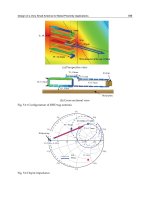
) is measured simultaneously using an infrared microscope (see
Figure 1-6), which has a spot size resolution as small as 1 mil in diameter. Nor-
mally, several readings are taken over the surface of the die and an average value
is used to specify T
j
.
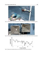
It is true that temperature over a die will vary typically 10 to 20ºC. A poorly
designed die (improper ballasting) could result in hot spot (worst case) tempera-
tures that vary 40 to 50ºC. Likewise, poor die bonds (see Figure 1-7) can result in
hot spots, but these are not normal characteristics of a properly designed and as-
sembled transistor die.
By measuring T
c
and T
j
along with P
o
and P
in
—both D.C. and RF—one can
calculate
JC
from the formula
JC
ϭ (T
j
Ϫ T
C
)/(P
in
Ϫ P
o
). Typical values for an
RF power transistor might be T
j
ϭ 130ºC, T
C
ϭ 50ºC; V
cc
ϭ 12.5 V, I
C
ϭ 9.6 A,
P
in
(RF) ϭ 10 W, and P
o
(RF) ϭ 50 W. Thus
JC
ϭ (130 Ϫ 50)/[10 ϩ (12.5 ϫ 9.6)
Ϫ 30] ϭ 80/80 ϭ 1ºC/W.
Several reasons dictate that a conservative value be placed on
JC
. First, ther-
mal resistance increases with temperature (and we realize T
C
ϭ 25ºC is NOT re-
10500_01_001-030_R3_jb.qxd 11/20/00 3:07 PM Page 6
Understanding RF Data Sheet Parameters 7
1
2
3
4
5
6
7
8
9
10
11
12
13
14
15
16
17
18
19
20
21
22
23
24
25
26
27
28
29
30
31
32
33
34
35
36
37
38
39
40
41
42
43
44
45Short
46Reg
FIGURE 1-6
Measurement of die temperature using an infrared microscope.
alistic). Second, T
j
is not a worst case number. And, third, by using a conser-
vative value of
JC
, a realistic value is determined for maximum P
d
. Generally,
Motorola’s practice is to publish
JC
numbers approximately 25% higher than
that determined by the measurements described in the preceding paragraphs, or
for the case illustrated, a value of
JC
ϭ 1.25ºC/W.
A few words are in order about die temperature. Reliability considerations dic-
tate a safe value for an all-Au (gold) system (die top metal and wire) to be 200ºC
(see Chapter 5, “Reliability Considerations”). Once T
j
max is determined, along
with a value for
JC
, maximum P
d
is simply P
d
(max) ϭ [T
j
(max) Ϫ 25ºC]/
JC
.
Specifying maximum P
d
for T
c
ϭ 25ºC leads to the necessity to derate maxi-
mum P
d
for any value of T
c
above 25ºC. The derating factor is simply the recip-
rocal of
JC
!
Maximum collector current (I
c
) is probably the most subjective maximum rat-
ing on the transistor data sheets. It has been, and is, determined in a number of
ways, each leading to different maximum values. Actually, the only valid maxi-
mum current limitations in an RF transistor have to do with the current handling
ability of the wires or the die. However, power dissipation ratings may restrict
current to values far below what should be the maximum rating. Unfortunately,
many older transistors had their maximum current rating determined by dividing
maximum P
d
by collector voltage (or by BV
CEO
for added safety), but this is not
a fundamental maximum current limitation of the part. Many lower frequency
parts have relatively gross top metal on the transistor die—that is, wide metal
runners and the “weak current link” in the part is the current handling capability
of the emitter wires (for common emitter parts). The current handling ability of
10500_01_001-030_R3_jb.qxd 11/20/00 3:07 PM Page 7
8 Radio Frequency Transistors
1
2
3
4
5
6
7
8
9
10
11
12
13
14
15
16
17
18
19
20
21
22
23
24
25
26
27
28
29
30
31
32
33
34
35
36
37
38
39
40
41
42
43
44
Short45
Reg46
FIGURE 1-7
Voids appear as dark spots in X-ray photographs and will lead to “hot spots” in die
temperatures.
wire (various sizes and material) is well known; thus, the maximum current rat-
ing may be limited by the number, size, and material used for emitter wires.
Most modern high frequency transistors are die limited because of high cur-
rent densities resulting from very small current-carrying conductors, and these
densities can lead to metal migration and premature failure. The determination of
I
c
max for these types of transistors results from use of Black’s equation for
metal migration,
3
which determines a mean time between failures (MTBF) based
on current density, temperature, and type of metal. At Motorola, MTBF is gener-
ally set at >7 years, while maximum die temperature is set at 200ºC. For plastic-
packaged transistors, maximum T
j
is set at 150ºC. The resulting current density,
along with a knowledge of the die geometry and top metal thickness and mate-
rial, allows the determination of I
c
max for the device.
It is up to the transistor manufacturer to specify an I
c
max based on which of
the two limitations (die or wire) is paramount. It is recommended that the circuit
design engineer consult the semiconductor manufacturer for additional informa-
tion if I
c
max is of any concern in the specific use of the transistor.
Storage temperature is another maximum rating that is frequently not given
the attention it deserves. A range of Ϫ55ºC to 200ºC has become more or less an
industry standard. And for the single metal, hermetic-packaged type of device,
the upper limit of 200ºC creates no reliability problems. However, a lower high
temperature limitation exists for plastic encapsulated or epoxy-sealed devices.
These should not be subjected to temperatures above 150ºC to prevent deteriora-
tion of the plastic material.
10500_01_001-030_R3_jb.qxd 11/20/00 3:07 PM Page 8
Understanding RF Data Sheet Parameters 9
1
2
3
4
5
6
7
8
9
10
11
12
13
14
15
16
17
18
19
20
21
22
23
24
25
26
27
28
29
30
31
32
33
34
35
36
37
38
39
40
41
42
43
44
45Short
46Reg
FIGURE 1-8
Test circuit for an RF power transistor.
POWER TRANSISTORS: FUNCTIONAL CHARACTERISTICS
The selection of a power transistor usually involves choosing one for a frequency
of operation, a level of output power, a desired gain, a voltage of operation, and a
preferred package configuration consistent with circuit construction techniques.
Functional characteristics of an RF power transistor are by necessity tied to a
specific test circuit (an example is shown in Figure 1-8). Without specifying a
circuit, the functional parameters of gain, reflected power, efficiency—even
ruggedness—hold little meaning. Furthermore, most test circuits used by RF
transistor manufacturers today (even those used to characterize devices) are de-
signed mechanically to allow for easy insertion and removal of the device under
test (D.U.T.). This mechanical restriction sometimes limits achievable device
performance, which explains why performance by users frequently exceeds that
indicated in data sheet curves. On the other hand, a circuit used to characterize a
device is usually narrow band and tunable. This results in higher gain than is at-
tainable in a broadband circuit. Unless otherwise stated, it can be assumed that
characterization data such a P
o
versus frequency is generated on a point-by-point
basis by tuning a narrow band circuit across a band of frequencies. It thus repre-
sents what can be achieved at a specific frequency of interest provided the circuit
presents optimum source and load impedances to the D.U.T.
Broadband, fixed tuned test circuits are the most desirable for testing func-
tional performance of an RF transistor. Fixed tuned is particularly important in
assuring everyone—the manufacturer and the user—of product consistency, that
is, that devices manufactured tomorrow will be identical to devices manufactured
today.
10500_01_001-030_R3_jb.qxd 11/20/00 3:07 PM Page 9