Advanced Radio Frequency Identification Design and Applications Part 2 potx
Bạn đang xem bản rút gọn của tài liệu. Xem và tải ngay bản đầy đủ của tài liệu tại đây (600.36 KB, 20 trang )
ratio of the actual power received by an antenna to the possible maximum received power
which can be accomplished by optimising the matching condition between the polarisation of
incident wave and that of receiving antenna. In mathematics, it is expressed as Equation 24
(Balanis, 2005),
e
p
=
|
l
e
· E
i
|
2
|l
e
|
2
|E
i
|
2
(24)
where
l
e
= vector effective length of the receiving antenna which has been introduced in Subsection
2.3,
E
i
= incident electric field.
UHF RFID systems usually adopt linearly polarised antennas as tag antennas because of their
low cost and easy fabrication. However, most RFID systems are used to detect mobile items,
for example, in the RFID application of supply chains, the cargo on which is mounted a tag
will be transported along a supply chain. If the reader antenna is linearly polarised, it is
possible that the tag antenna and the reader antenna can be aligned orthogonally to each other.
When that happens, the reader will not be able to read or program RFID tags. Hence, RFID
reader antennas often adopt circular polarisation to ensure in most of the cases the system can
perform correctly. As a result, the polarisation efficiency between a reader antenna in circular
polarisation and a tag antenna in linear polarisation is 0.5 i.e. -3dB.
2.7 The Friis transmission equation
After introducing the fundamental parameters for describing an antenna, the Friis
transmission equation commonly used in designing and analysing communication systems
is given in Equation 25. This equation relates the power delivered to the load of a receiving
antenna P
r
to the available power P
t
from a transmitter which is placed at a distance r >
2D
2
/λ in free space, where D is the largest dimension of either antenna.
P
r
= P
t
(1 −|Γ
t
|
2
)(1 −|Γ
r
|
2
)g
t
g
r
(
λ
4πr
)
2
e
p
(25)
In Equation 25, Γ
t
, Γ
r
are the reflection coefficients of the transmitting antenna and the
receiving antenna respectively, g
t
and g
r
are the gain of the transmitting and the receiving
antenna respectively, as defined in Subsection 2.4, and e
p
denotes the polarisation efficiency
which is explained in Subsection 2.6.
If the two antenna’s impedances are perfectly matched to their source or load and their
polarisation is matched as well, an ideal form of Equation 25 is expressed as follows.
P
r
= P
t
g
t
g
r
(
λ
4πr
)
2
(26)
Equation 25 is an idealised form of the Friis transmission equation. When this equation is
applied in analysing RFID systems, a few changes should be made according to the special
needs of RFID systems, which are identified in Section 7.
In addition, the factor
(
λ
4πr
)
2
which is defined as the path gain describes the dependence of
the power received by the transponder on the wavelength and the distance r. Normally, this
factor is much less than 1, and we speak of there being a loss. However, this path loss occurs
in free space. Most of RFID systems are installed in a building or even a room. Therefore, the
path loss in a more complicated environment should be considered before applying it to an
RFID system. The evaluation of the in-building path loss has been described in Section 7.
9
Operating Range Evaluation of RFID Systems
3. Tag antenna design
In Section 2, a few fundamental parameters such as gain, impedance match, polarisation
etc, in designing antennas are discussed. Besides those parameters, some other parameters
e.g. the antenna size, cost and deployed environment should be considered as well if the
antenna is expected to be used in reality. Usually, the tag antenna design is more limited
by those parameters required by the reality than the reader antenna design, hence only the
tag antenna design is discussed in this section. The parameters required by the reality are
discussed respectively in the three following itemisations.
• Size
Generally for tag antennas the smaller the better. However, the small size will also affect
other factors, such as gain, impedance match and bandwidth. Most of the commercial tags
are less than 140mm
×40mm.
• Applied environment or attached objects
Definitely, an RFID system will not be deployed in free space. The applied environment
especially when a tag is attached to a metallic object will have a critical impact on the
performance of the RFID system because of the metallic boundary conditions. As a result,
a solution to this problem is needed before completing an antenna design.
• Cost
Generally speaking, a 96-bit EPC inlay (chip and antenna mounted on a substrate) costs
from 7 to 15 U.S. cents (RFID Journal, 2010). Low cost tags are always required by the
industry for a wide range of applications. One of the possible solutions to reduce the cost
significantly is the use of printed electronics, especially printed silicon electronics, which
is out of the scope of the work in this chapter. Cole et al. (2010) give more details of the
printed electronics and its costs.
Unfortunately and not surprisingly, the factors discussed in this section and the antenna
parameters discussed in Section 2 are interacting and usually are not positively related. Some
tradeoffs, depending on the system requirements, should be made during the antenna design.
4. Threshold power of a transponder
Chips require a minimum power or voltage to be operated which are called threshold power
or threshold voltage. Generally, the threshold power is about 100μW (Finkenzeller, 2003) but
canbeevenlessdownto16.7μW (Karthaus and Fischer, 2003). If the distance between a tag
and a reader is too far for the tag to collect more power than the threshold, that tag is unable
to be detected. The amount of power or voltage, which can be collected by transponders at
a certain distance, depends on the tag antenna design which is briefly discussed in Section 3.
Apparently, this threshold is critical to evaluate the reading range of an RFID system and it
is definitely decided by the chip IC design. As shown in Figure 4, a typical transponder IC
consists of several principal components which are decoder, voltage multiplier, modulator,
control logic and memory unit. Each component’s power consumption or power transfer
efficiency can influence the threshold power. These factors are discussed in the subsections
below.
10
Advanced Radio Frequency Identification Design and Applications
Decoder
Modulator
Voltage
Multiplier
Memory
Units
Logic
V
DD
data
data
data
Antenna
Front end
clk
Fig. 4. Block chart of a transponder.
4.1 Modulator
The power transfer efficiency influenced by impedance matching situation has been analysed
in Subsection 2.1. If the ideal impedance match is obtained which means the chip input
impedance is the complex conjugate of the antenna impedance, half of the captured power is
delivered to the chip, the other half is consumed by the antenna linked to the chip. However,
in this case, the signals carrying backscattered power are all in the same phase and magnitude,
and cannot carry any information. Therefore, a modulator is employed in the chip circuit to
adjust the front-end impedance into two different states, Z
chi p1
and Z
chi p2
.Hence,phaseor
magnitude of the backscattered wave can be changed to form a useful signal back to the base
station antenna. The input RF power to the chip becomes Equation 27.
P
chi p
r,1,2
= P
A
(1 −|θ
1,2
|
2
) (27)
where
θ
1,2
=
Z
chip1,2
−Z
∗
tant
Z
chip1,2
+Z
tant
,
P
A
=maximum available power.
The power reflected from the chip for backscattering also then varies between two states
according to Equation 10. In terms of the modulation modes, ASK (Amplitude Shift Keying)
or PSK (Phase Shift Keying) could be employed. For ASK, the amplitude difference of the
backscattered wave between the two states brought by θ
1
, θ
2
should be large enough to allow
the reader to tell them apart. Similarly, for PSK, the phase difference of the backscattered
wave between the two states brought by θ
1
, θ
2
should be large enough to allow the reader to
tell them apart. The difference of the two states determines the error probability.
As a result, the θ parameter is a decisive factor in designing an RFID system. It determines
through Equation 27 how much RF power is distributed to the chip rectifier to be converted
into dc power and through Equation 10 how much RF power is assigned to backscatter to
the reader for it to decode under a particular modulation mode either ASK or PSK. The
optimisation of the two states of θ depending on the modulation modes to achieve the best
usage of the RF power received by the transponder is discussed by Karthaus and Fischer
(2003). The selection of the two states of θ under either ASK mode or PSK mode for obtaining
reading range oriented RFID system or bit-rate oriented RFID system is reported by Vita et al.
11
Operating Range Evaluation of RFID Systems
(2005). The task of optimising the factor of θ is out of the scope of the work in this chapter.
Hence, it is not discussed further.
4.2 Rectifier efficiency
Once the RF power is received, it will be transmitted to the inside circuit, including voltage
multiplier, decoder, control logic and memory units. However, the RF power cannot be used
by these components directly and the induced voltage in the terminal of the tag antenna is too
small to excite the circuit. As a result, a voltage multiplier is needed to rectify the ac current
to dc, and to enlarge the induced ac voltage. This process definitely brings power loss due
to the diode and capacitor composing of multiplier. The ratio of dc power produced by the
voltage multiplier to the input RF power is called rectifier efficiency. Clearly, threshold power
will be increased by a low rectifier efficiency. It was reported that rectifier efficiency ranged
from 5-25% (Finkenzeller, 2003). For example, Karthaus and Fischer (2003) achieved a 18%
rectifier efficiency. However, with the recent years development of semiconductor technology
and circuit design, rectifier efficiency has been improved significantly. Nakamoto et al. (2007)
even made the factor to be 36.6%.
4.3 Memory chosen
The threshold power, can be divided into two types: 1) the threshold power for reading and
2) the threshold power for programming. Those two types of threshold power are also related
to the memory which is used to store data in the transponder. The data carriers, currently
applied, can be categorised into the three types of RAM, EEPROM as well as FeRAM. A
comparison among these memories is made below:
• RAM
This kind of memory can store data only temporarily. When the voltage supply disappears,
the stored data is lost. This form of memory can be used in a passive tag as a temporary
information storage when the tag is being read or written. Additionally, it can also be
applied in an active tag.
• EEPROM
Compared to RAM, EEPROM is a long-term storage memory which can provide reliable
data for around ten years (Finkenzeller, 2003). The reading operation with this memory
needs a relative low supply voltage which is usually below 5V (Finkenzeller, 2003;
Karthaus and Fischer, 2003). Che et al. (2008) even succeed in lowering the threshold
voltage to be 0.75V. Moreover, a considerably large voltage (around 17V) is needed to
activate the tunnel effect, so that data can be written. Although a charging pump is
integrated into the circuit to provide this large voltage and EEPROM is used widely as
an RFID tag memory, it still has two serious weakness. Firstly, the power consumption
of programming is much lager than that of reading due to the large voltage needed in
writing. As a result, the tag integrated with EEPROM cannot be read and written at the
same range. Usually, the writing range is only about 20% of the reading range. Secondly,
the programming is a time-expensive operation due to the tunneling principle (Nakamoto
et al., 2007). In general, it needs 5-10ms for each single-bit or multiple-bit operation.
• FeRAM
FeRAM is invented to solve the weaknesses which are faced by EEPROM. The ferroelctric
effect is taken advantage of to store data and achieve a balanced power consumption in
both reading and programming. In particular, Nakamoto et al. (2007) addressed this
12
Advanced Radio Frequency Identification Design and Applications
unbalanced reading and writing barriers by employing FeRAM memory. The writing time
is also improved to 0.1μs (Finkenzeller, 2003; Nakamoto et al., 2007). A 4m operating
distance approximately balanced in reading and writing was derived for a 4W EIRP
transmitted power. The actual input power of both working modes is nearly the same
which are 13μW in reading and 15.7μW in writing. The writing speed of FeRAM is 100
times faster than that of EEPROM. However, FeRAM has not been widely used in place
of EEPROM because FeRAM cells are difficult to combine with CMOS processes, since a
high temperature treatment is needed to crystallise the memory materials (PZT or SBT)
into ferroelectric phases before the cell is connected to the CMOS (Finkenzeller, 2003; Lung
et al., 2004).
Table 1 provides a comparison among the three memories (Finkenzeller, 2003; Fujitsu, 2006).
Comparison parameters RAM EEPROM FeRAM
Size of memory cell ∼ ∼130( μm)
2
∼80( μm)
2
Lifetime in write cycles ∞ 10
5
10
10
∼ 10
12
Read cycle (ns) 12 ∼ 70 200 110
Write cycle 12∼70ns 3∼10ms 0.1μs
Data write Overwrite Erase + Write Overwrite
Write voltage (V) 3.3 15 ∼ 20 2 ∼ 3.3
Energy for Writing ∼ 100μJ 0.0001μJ
Table 1. Comparison among RAM, EEPROM and FeRAM.
In conclusion, as long as the modulation mode, the rectifier efficiency, the dc power needed by
the chip circuit and the type of memory units are known, the threshold power of transponder
can be derived. In particular, Karthaus and Fischer (2003) made a tag which could be read
at a distance of 4.5m under only 500mW ERP radiated power. In this case with on-wafer
measurements, the rectifier efficiency was established to be 18%, the dc power consumed
by the chip circuit was 2.25μW(1.5μA, 1.5V). As a result, the minimum input RF power for
operation is 12.5μW(
2.25μW
18%
). The threshold RF power for reading is the sum of the minimum
backscattered power (4.2μW) derived by Karthaus and Fischer (2003), and the minimum input
RF power (12.5μW). However, the threshold power for programming is much larger than
that for reading because an EEPROM memory is chosen which choice leads to an unbalanced
operating range between reading and programming. The optimisation of all factors discussed
in this section is beyond our work, so they will not be discussed further in this chapter.
5. The reader sensitivity
Young (1994) gave the mathematical expression of a general receiver’s sensitivity, and is
reproduced as follows.
Sen
=(S/N)
min
kTB(NF) (28)
where
Sen = sensitivity,
(S/N)
min
= the minimum signal to noise ratio required to demodulate the replying signal,
k = Boltzman’s constant,
B = bandwidth of the receiver,
NF = noise factor of the receiving equipment,
T = absolute reference temperature used in the definition of the noise factor.
In the case of an RFID reader the sensitivity can be influenced by several additional factors
13
Operating Range Evaluation of RFID Systems
including receiver implementation details, receiver gain, communication protocol specifics
and interference generated both within the reader and externally by other users of the
spectrum. A figure for sensitivity is usually available from the reader manual, and is
commonly -70dBm. However, for passive tags the sensitivity is usually good enough for
detecting the backscattered signal (Nikitin and Rao, July 2006), and the range is limited by
tag excitation, not receiver sensitivity.
6. The literature review on the existing work in evaluating operating range
Significant work has been done in evaluating operating range of RFID systems recent years.
Griffin et al. (2006) reported two radio link budgets based on the Friis equation. The first
budget links the power received by a chip to the power radiated from a reader antenna.
The second budget establishes the relationship between the power received by the reader
from the backscattered power of the tag and the power radiated from the reader antenna.
The contribution of Griffin et al. (2006) is to add a new factor named as gain penalty
in the modified Friis transmission equation. The gain penalty shows to what extent the
materials close to the tag can reduce the antenna’s gain. However, Griffin et al. (2006)
assumes the tag antenna’s impedance is always matched to the chip. This is not an
accurate assumption because 1) the requirement of the modulation needs at least one state of
impedance mismatching, 2) the existence of electro-magnetically sensitive materials in close
proximity to the tag will critically vary the output impedance of the tag antenna (Dobkin and
Weigand, 2005; Prothro et al., 2006).
Nikitin and Rao (December 2006) introduced a new method in describing and measuring the
backscattered power from the tag antenna by means of radar cross section (RCS) based on the
Friis transmission equation in free space. Compared with the study by Griffin et al. (2006), the
impedance mismatch occurring in the tag and caused by the modulation is considered. The
RCS of a meander line dipole antenna in three different situations is investigated by assuming
the antenna is placed in free space. The three situations are 1) the antenna is loaded with a
chip, 2) the antenna is shorted and 3) the antenna is open circuit. The measurement of the RCS
was thus conducted in an anechoic chamber after background substraction. However, when
the tag is deployed in a more complicated environment than in free space, this method is not
applicable.
Jiang et al. (2006) proposed another concept response rate in evaluating the operating range of
an RFID system by experiments. Most of the exciting readers support a “poll" mode, wherein
the reader continually scans for the presence of RFID tags. For example, a reader sends N
polls within a second, and counts the number of the responses (N
r
) from the particularly tag
being observed. Therefore, the response rate from that tag is defined as α
= N
r
/N.Thelarger
the response rate is, the more probability the tag will be read. By placing the tag in different
positions each time in a complex environment, and counting the response rate of the tag, the
readable probability of the tag in various positions can be derived. The optimum position
could be found and this optimisation definitely involves the influence of the environment. In
addition, people can even place many tags in the complex environment at one time and get
the response rate of each tag by experiments. The method not only considers the effects from
the environment but also the effects from the mutual coupling among the tags.
Hodges et al. (2007) optimised the position where the tag should be attached on each bottle of
wine within a case containing six identical bottles based on a modified response rate test. The
test is modified by setting a threshold response rate and attenuating the transmitting power
from the reader programmablly to meet that threshold response rate. Then the RF margin for
14
Advanced Radio Frequency Identification Design and Applications
the tag in each location on the wine bottle is tested and the optimum location is determined.
According to the discussion above, the existing work is based on either theoretical analysis
according to the Friis equation or totally experimental analysis in a real RFID system. The
experimental analysis is a direct solution but may be expensive in cost or in time. In addition,
the limitation of using the Friis equation is also obvious in that it cannot deal with a complex
environment. More details of the Friis equation’s limitation in evaluating the operating range
of an RFID system are given in Section 7.
Furthermore, the simulation tools such as Ansoft HFSS or CST can accomplish a full wave
analysis on the transmission between two antennas or among multiple antennas. A complex
environment can be built in the simulation model and considered in the simulation process.
The accomplishment of the simulation is definitely dependent on the computing ability of
the equipment used. The influences of the environment on the antenna gains and input
impedance can be obtained directly, hence people may argue that the Friis equation could
still be used combining with the simulation results about the antenna impedance and gain
which is similar to what Griffin et al. (2006) did by involving a gain penalty, but the path
loss caused in the propagation cannot be obtained directly which is required by the Friis
transmission equation. Hence, we totally abandon the Friis equation but turn to evaluating
the reading range of an RFID system in any environment by a scattering matrix which takes
all the relevant matters into account. More importantly, a scattering matrix can be obtained
by both simulation and experiments. This novel method in evaluating the operating range of
an RFID system is introduced in Section 8.
7. Interpretation and limitations of the Friis transmission equation in an RFID
perspective
In Subsection 2.7, a common form of the Friis transmission equation is given in Equation 25.
In addition, Equation 25 is simplified to Equation 26 in an ideal condition. In this section, the
physical meaning of each factor in the Friss transmission equation and its usage is interpreted
in an RFID perspective. With respect to the radio wave communication between a reader
and a passive tag, it is known that the reader firstly interrogates the tag, which is named as
forward-link. Then, the tag receives the power from the interrogating wave and makes use
of this power to backscatter a signal to the reader, which process is named as backward-link.
The Friis transmission equation may be used once in each link. We therefore discuss the use
of the Friis transmission equation in the two links respectively and identify its limitations in
analysing operating range of an RFID system.
7.1 Forward link
In the forward-link, the reader antenna is in the transmitting mode. Conversely, the tag
antenna is in the receiving mode. The Friis transmission equation used in this link is written
as follows according to Equation 25.
P
chi p
r
= P
reader
t
(1 −|Γ
rant
|
2
)(1 −|θ|
2
)g
reader
g
tag
1
pl
e
p
(29)
P
reader
t
represents the available source power from the reader generator, which has been
designed to produce optimum power into a load of real impedance Z
0
and has been connected
to the reader antenna by a cable of characteristic impedance Z
0
. P
chi p
r
is the power received
by the chip. Γ
rant
is the reflection coefficient between the reader antenna and the reader which
15
Operating Range Evaluation of RFID Systems
is expressed in Equation 30a. Z
rant
is the input impedance of the reader antenna, Z
0
is the
characteristic impedance of the transmission line connected to the reader antenna, which is
usually 50Ω. θ is the parameter the magnitude squared of which describes the fraction of
the available source power not delivered to the tag circuit as defined in Subsection 2.1 and
rewritten in Equation 30b in which Z
chi p
is the chip impedance, Z
tant
is the output impedance
of the tag antenna and Z
∗
tant
is conjugate to Z
tant
. g
reader
and g
tag
are the gains of the reader
antenna and the tag antenna respectively. The path gain factor
(
λ
4πR
)
2
in Equation 25 is
changed to be
1
pl
, since the RFID system considered here is not assumed to be operated in
free space but a more practical and complex environment.
Γ
rant
=
Z
rant
− Z
0
Z
rant
+ Z
0
(30a)
θ
=
Z
chi p
− Z
∗
tant
Z
chi p
+ Z
tant
(30b)
The expression of the power input into the reader antenna is given in Equation 31 according
to Equation 21.
P
rant
t
= P
reader
t
(1 −|Γ
rant
|
2
)=
P
EI RP
g
reader
(31)
where P
EI RP
is the equivalent isotropic radiated power which meaning is given in
Subsection 2.5. The involvement of P
EI RP
is because the maximum power allowed to be
radiated is usually described in terms of P
EI RP
. According to Equation 31, Equation 29
becomes:
P
chi p
r
= P
EI RP
(1 −|θ|
2
)g
tag
1
pl
e
p
(32)
The maximum value of P
chi p
r
is obtained when P
EI RP
is set to be maximum which is regulated
differently in different countries and regions. To make the tag readable, P
chi p
r
has to be larger
than the threshold power for operating the chip, which was discussed in Section 4.
In Equation 7, another form of P
chi p
r
is given in terms of maximum available power P
A
and
the theta parameter θ, which is rewritten as follows.
P
chi p
r
= P
A
(1 −|θ|
2
) (33)
7.2 Backward link
In the backward-link, the tag antenna is in the transmitting mode. Conversely, the reader
antenna is in the receiving mode. The Friis transmission equation used in this link is written
as follows.
P
reader
r
= P
tag
sum
(1 −|Γ
rant
|
2
)g
reader
g
tag
1
pl
e
p
(34)
where P
reader
r
is the power received by the reader and P
tag
sum
is the sum of the powers dissipated
within and backscattered from the tag antenna. The expression of P
tag
sum
has been given in
Equation 9 which is rewritten in Equation 35. The path loss factor remains the same as that
in Equation 32, since the propagating path in the forward link is the same as in the backward
link.
P
tag
sum
= P
A
|1 − θ|
2
(35)
16
Advanced Radio Frequency Identification Design and Applications
Solving for P
chi p
r
according to Equation 35 and Equation 33 gives:
P
chi p
r
=
1 −|θ|
2
|1 − θ|
2
P
tag
sum
(36)
Substituting Equation 36 into Equation 29, another expression of P
tag
sum
is derived.
P
tag
sum
= P
reader
t
(1 −|Γ
rant
|
2
)|1 − θ|
2
g
reader
g
tag
1
pl
e
p
(37)
Substituting Equation 37 into Equation 34, then
P
reader
r
= P
reader
t
[(1 −|Γ
rant
|
2
)|1 − θ|g
reader
g
tag
1
pl
e
p
]
2
(38)
Equation 38 establishes the relationship between the power transmitted from the reader P
reader
t
and the power received by the reader P
reader
r
after the transmitted wave is backscattered from
the tag antenna. P
reader
r
has to be larger than the sensitivity of the reader which was introduced
in Section 5.
According to Equation 31, P
reader
t
is replaced by P
EI RP
/[(1 −|Γ
rant
|
2
)g
reader
], Equation 38
becomes:
P
reader
r
= P
EI RP
(1 −|Γ
rant
|
2
)g
reader
[|1 − θ|g
tag
1
pl
e
p
]
2
(39)
7.3 Limitations in implementing the Friis transmission equation
In Subsections 7.1 and 7.2, the power transfer between the transponder and the reader in the
forward and backward link is established in Equation 29 and Equation 38 by means of the
Friis transmission equation.
However, there are a few limitations in implementing the Friis transmission equations for
evaluating the operating range of an RFID system, if the system is deployed in a very complex
environment, e.g. 1) when a tag is mounted on a metallic item or a liquid item, or 2) when the
testing environment contains a lot of metal reflectors. The reasons of the limitations are given
as follows.
1. Far field condition
To implement the Friis transmission equation, the two antennas in communication should
be sufficiently far away from each other. The distance between them should be larger
than 2D
2
/λ,whereD is the largest dimension of either antenna, and λ is the free space
wavelength at the resonant frequency. However, when an RFID system is placed in the
very complex environment as mentioned before, the reader antenna has to be very close to
the tag in order to read it. Hence, the distance between them is not sufficient to meet the
far field criterion.
2. Gain and impedance variation
In the Friis transmission equation, the gain and input/output impedance of the tag/reader
antenna are involved. However, again the RFID system is placed in a very complex
environment. The gain pattern and impedance will vary from the intentionally designed
values. The effects brought by metals in proximity to a tag antenna to the antenna’s
output impedance and gain are discussed by Griffin (2006) and Dobkin (2005). It would be
possible to investigate those effects by means of simulation or experiments, but that would
require effort.
17
Operating Range Evaluation of RFID Systems
3. Unknown path loss factor
As shown in Equation 31 and Equation 38, path loss factor
1
pl
is still unknown. If the RFID
system is deployed in free space,
1
pl
is equal to (
λ
4πr
)
2
,wherer is the distance between the
two communicating antennas. Most RFID systems are not deployed in free space but in
an in-building environment consisting of many obstacles in the signal propagating path,
and the system may be composed of multiple readers and tags. Because of the obstacles in
building-environment where an RFID system is deployed, there are more losses brought
by path obstruction, reflection, multi-path propagation, absorption and other attenuation
effects. In addition, there are also more losses brought by the interaction between the
multiple readers and tags.
The analysis of path loss of a dense reader environment was given by Leong (2008). The
path loss in dB of a two-antenna RFID system (one tag antenna, one reader antenna) in
building is introduced (Rappaport, 2002):
PL
(dB)=PL(d
0
)+10 × n × log
10
(
d
d
0
) (40)
where d
0
is an arbitrary reference distance; n is a value that depends on the surroundings
and building type; d is the distance between the reader antenna and the tag antenna. The
reference distance d
0
should be selected to be much smaller than the size of the building,
so that the reflection in this small distance is not significant and the path loss in this small
distance d
0
can be considered approximately equal to the path loss in free space.
Path loss represented by Equation 40 is a rough evaluation of the general case of an RFID
system in building. It does not have the universality of all situations and especially is not
suitable for defining the path loss factor in complex environments, e.g. metallic items in
near proximity to a tag.
Based on the limitations in implementing the Friis transmission equation in evaluating the
operating range of an RFID system, a novel method by means of the scattering matrix is
therefore proposed in Section 8.
8. The use of S-parameters in analysing the operating range of RFID systems
8.1 Formula derivation
We consider the two antennas (a reader antenna and a tag antenna) transmission system to be
a two port system, as shown in Fig. 5, in which the reader and chip are connected to the reader
antenna and the tag antenna by transmission lines of which the characteristic impedance is
Z
0
. In Fig. 5, the reader antenna is represented by the two thick lines in the dashed circle
for which the input impedance, taking into account the coupling between the antennas, is
Z
rant
, and the tag antenna is represented by the two thin lines in the dashed circle for which
the output impedance, taking into account the coupling between the antennas, is Z
tant
.The
resistance of the reader R
reader
is deliberately designed to be equal to Z
0
(50Ω). In addition,
the transmission line between the tag and the chip is very short.
In the following discussion, we will make use of scattering parameters to establish the
relationship between the power received by the chip and the power transmitted from the
reader antenna. All the values involving voltage and current are represented by peak value
phasors.
18
Advanced Radio Frequency Identification Design and Applications
V
in
R
chip
X
chip
R
reader
Port 2
V
1
+
V
1
-
V
2
+
V
2
-
Z
0
Z
0
Port 1
Z
rant
Z
tant
I
1
V
1
I
2
V
2
V
0
+
V
0
-
Port 0
Fig. 5. Two port junction representing coupled antennas in an RFID system.
On the right side of Fig. 5, the voltage V
0
and current I
0
at the load port are expressed in
Equation 41.
V
0
= V
+
0
+ V
−
0
(41a)
I
0
= I
+
0
+ I
−
0
(41b)
The current I
+
0
and I
−
0
can also be expressed by the voltage in and out of the load port as
shown in Equation 42.
I
+
0
=
V
+
0
Z
0
(42a)
I
−
0
= −
V
−
0
Z
0
(42b)
The ratio of V
−
0
/V
+
0
is equal to the reflection coefficient looking into the chip impedance from
the terminal of the transmission line, which is written as follows.
V
−
0
V
+
0
= s
L
=
Z
chi p
− Z
0
Z
chi p
+ Z
0
(43)
The power received by the chip P
chi p
r
is obtained by Equation 44.
P
chi p
r
=
|
I
0
|
2
2
R
chi p
=
1
2
|
V
0
Z
chi p
|
2
R
chi p
=
|
V
+
0
+ V
−
0
|
2
R
chi p
2|Z
chi p
|
2
=
|
V
+
0
|
2
|1 + s
L
|
2
R
chi p
2|Z
chi p
|
2
(44)
As mentioned before, the transmission line between the chip and the tag antenna is very
short (its length is nearly zero), hence, V
+
0
= V
−
2
and V
−
0
= V
+
2
. Then Equation 43 becomes
19
Operating Range Evaluation of RFID Systems
Equation 45. In addition, replacing V
+
0
in Equation 44 by V
−
2
, Equation 46 is derived.
V
+
2
V
−
2
= s
L
=
Z
chi p
− Z
0
Z
chi p
+ Z
0
(45)
P
chi p
r
=
|
V
−
2
|
2
|1 + s
L
|
2
R
chi p
2|Z
chi p
|
2
(46)
Similarly, on the left side of Fig. 5, the voltage V
1
and current I
1
on the port one is expressed
in Equation 47.
V
1
= V
+
1
+ V
−
1
(47a)
I
1
= I
+
1
+ I
−
1
(47b)
The current I
+
1
and I
−
1
can also be expressed by the voltage in and out of the port one as shown
in Equation 48.
I
+
1
=
V
+
1
Z
0
(48a)
I
−
1
= −
V
−
1
Z
0
(48b)
TheratioofV
−
1
/V
+
1
is equal to the reflection coefficient Γ
rant
which is expressed in Section 7
and rewritten as follows.
V
−
1
V
+
1
= Γ
rant
=
Z
rant
− Z
0
Z
rant
+ Z
0
(49)
The power transmitted from the reader antenna P
rant
t
is obtained by Equation 50.
P
rant
t
=
1
2
Re
(V
1
· I
∗
1
)=
1
2
Re
[
1
Z
0
(V
+
1
+ V
−
1
)(V
+
1
− V
−
1
)
∗
]
=
1
2
Re
[
1
Z
0
|V
+
1
|
2
(1 + Γ
rant
)(1 − Γ
rant
)
∗
]=
|
V
+
1
|
2
2Z
0
(1 −|Γ
rant
|
2
) (50)
A scattering matrix can be built according to the simplified two port system shown in Fig. 5
as below.
V
−
1
V
−
2
=
s
11
s
12
s
21
s
22
V
+
1
V
+
2
(51)
According to the above matrix, the V
−
1
and V
−
2
can be written into Equation 52.
V
−
1
= s
11
V
+
1
+ s
12
V
+
2
(52a)
V
−
2
= s
21
V
+
1
+ s
22
V
+
2
(52b)
Substituting the first of Equation 45 and Equation 49 into Equation 52, solving for V
−
1
/V
+
1
and
V
−
2
/V
+
1
gives
V
−
1
V
+
1
= Γ
rant
= s
11
−
s
12
s
21
s
L
s
22
s
L
− 1
(53)
20
Advanced Radio Frequency Identification Design and Applications
V
−
2
V
+
1
=
s
21
1 − s
22
s
L
(54)
Hence,
V
−
2
= V
+
1
s
21
1 − s
22
s
L
(55)
Equation 53 illustrates how the impedance mismatch in the transponder and the testing
environment considered in the S parameters affect the reflection occurring between the reader
and the reader antenna.
Inserting Equation 55 into Equation 46:
P
chi p
r
=
|
V
+
1
|
2
|s
21
|
2
|1 + s
L
|
2
R
chi p
2|1 − s
22
s
L
|
2
|Z
chi p
|
2
(56)
Equation 56 demonstrates that the power received by the chip is partially related to
|V
+
1
|
2
.The
value of
|V
+
1
|
2
can be defined by the combination of Equation 31 and Equation 50 as follows:
P
rant
t
=
|
V
+
1
|
2
2Z
0
(1 −|Γ
rant
|
2
)=
P
EI RP
g
reader
(57)
Then Equation 56 becomes:
P
chi p
r
=
P
EI RP
g
reader
|s
21
|
2
R
chi p
Z
0
|Z
chi p
|
2
|1 + s
L
|
2
(1 −|Γ
rant
|
2
)|1 − s
22
s
L
|
2
(58)
In Equation 57,
|V
+
1
|
2
2Z
0
represents the available source power from the reader generator. The
product of this power and
(1 −|Γ
rant
|
2
) denotes the power radiated from the reader antenna.
This radiated antenna power can be expressed in terms of P
EI RP
by multiplying by the gain of
the reader antenna g
reader
.IfP
EI RP
is set to be the maximum power specified by regulations,
then Equation 57 tells us that no matter what the reflection between the reader antenna and
the transmission line is, the reader antenna can always be made to radiate the same amount
of power
P
EIRP
g
reader
by adjusting the available source power
|V
+
1
|
2
2Z
0
.
Finally, the power received by the chip is represented by means of scattering parameters
which can be obtained by the simulation tools or experiments. The complex environment in
which the RFID system is deployed can be built in the simulation model and considered in the
simulation process. In terms of experiments, the environment is certainly considered. P
EI RP
is specified by the regulations in different countries and regions separately. In Australia, this
factor is equal to 4W or 36dBm as introduced before. g
reader
is dependent on the reader antenna
deployed. s
L
can be calculated by Equation 43. The reflection occurring between the reader
and the reader antenna represented by Γ
rant
is caused by the testing environment represented
by S parameters and s
L
as shown in Equation 53. As a result, P
chi p
r
can be obtained. When P
chi p
r
is less than the threshold power of the chip which is in the order of -10dBm, the reading fails
and the maximum reading range can be read in the simulation model or measured directly in
experiments. Here, the backward link is not considered since it is concluded (Nikitin, 2006)
that the limitation of the reading range of a passive RFID systems mainly comes from the
forward link not the backward link because usually the reader’s sensitivity is, as mentioned
before, low enough to detect the signal from the successfully excited tag.
21
Operating Range Evaluation of RFID Systems
8.2 Formula validation
In the last subsection, Equation 58 has been derived to calculate the power received by the
chip. In this subsection, it is verified by simulation and experiments. However, as mentioned
before, to implement Equation 58, the available source power of the reader generator
should be adjusted according to Γ
rant
to keep the radiation power from the reader antenna
as P
EI RP
/g
reader
. The implemented condition brings some obstacles in the experimental
validation, since the available source power of most real reader generators cannot be adjusted
arbitrarily. The available source power can only be set stage by stage and the gap between the
adjacent stages is large (in our case the gap is 0.1W).
The approach we adopted to solve that problem is to keep the available source power
unchanged as P
EI RP
/g
reader
which is very easy to achieve by the real reader and leads to:
|V
+
1
|
2
2Z
0
=
P
EI RP
g
reader
(59)
After substituting Equation 59 into Equation 56:
P
chi p
r
=
P
EI RP
g
reader
|s
21
|
2
R
chi p
Z
0
|Z
chi p
|
2
|1 + s
L
|
2
|1 − s
22
s
L
|
2
(60)
Equation 60 is more convenient to be used in the form of dB, which is shown in Equation 61.
P
chi p
r
(dBm)=P
EI RP
(dBm) − G
reader
(dBi)+|S
21
|(dB)
+
10 log
10
R
chi p
Z
0
|Z
chi p
|
2
+ 20 log
10
|
1 + s
L
1 − s
22
s
L
| (61)
In the following discussion, Equation 58 is verified indirectly by verifying Equation 61 by
simulation and experiments. The experiments were conducted by testing the reading range
of a self-made tag. The equipment used in the experiments is introduced first.
• Self-made tag
The self-made tag shown in Fig. 6 is used. The chip is manufactured by Alien Technology
which model is Higgs-2. The chip conforms to the EPCglobal Class 1 Gen 2 specifications.
It is implemented in a CMOS process and uses EEPROM memory. The equivalent input
impedance of the chip in parallel is shown in Fig. 7(a) in which the parallel resistance
R
p
is 1500Ω and the parallel capacitance C
p
is 1.2pF. Usually, the input impedance of a tag
antenna is presented in series. Hence, in order to simplify the analysis, the chip impedance
is transformed into a series representation, so Fig. 7(a) becomes Fig. 7(b). At 923MHz which
is the centre frequency of UHF RFID band in Australia, the input impedance in series is
about 13.6-j142Ω.Hence,Z
chi p
in Equation 61 can be obtained. Typically the threshold
power of this chip is -14dBm, but the threshold power is dependent on the manufacturing
quality control, the worst could be -11dBm. More details of the chip can be found in the
product data sheet (Alien Technology, 2008).
The tag antenna is a meander line dipole antenna fabricated on FR4 board which thickness
is 1.6mm and the dielectric constant is 4.4. The footprint of this antenna is 43.8
×28.8 (unit
mm). The output impedance of this antenna is designed to be approximately conjugate
matched to the chip impedance.
The chip is installed on the antenna by electrically conductive adhesive transfer tape
22
Advanced Radio Frequency Identification Design and Applications
9703 manufactured by 3M (3M, 2007). Currents can pass perpendicularly through the
sticky tape. The tape and adhesive material on it will bring losses and chip impedance
changes. However, previous experiences with this tape reported by other colleagues in our
laboratory indicated that these losses and impedance changes are negligible (NG, 2008).
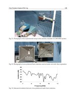
Fig. 6. A self-made tag used in experiment.
A
B
C
p
R
p
(a) In parallel
A
B
C
s
R
s
(b) In series
Fig. 7. The chip impedance illustration.
• Reader
The RFID reader used in the experiment is manufactured by FEIG Electronics which model
is ID ISC.LRU2000. The reader antenna is the linearly polarised patch antenna with 8dBi
gain and manufactured by Cushcraft Corporation, model: S9028P. The reason why the
linearly polarised reader antenna is used is to simplify the model building in the simulation
discussed later.
• Shielding tunnel
The reading range experiments were conducted by placing both the self-made tag and the
reader antenna inside of a shielding tunnel. The size of the tunnel is 1826
×915×690 (unit
mm), which is shown in Fig. 8. The shielding tunnel is surrounded by electromagnetic
wave absorbing foam. The absorbing foam is manufactured by the Emerson & Cuming
company for the frequency range from 600MHz to 4GHz. These absorbing foams can
achieve maximum -22dB reflectivity around 1GHz. The inside space of the tunnel can thus
be considered to be effectively free space.
As mentioned before, the reading range of the self-made tag were measured by placing the
tag and the reader antenna in the shielding tunnel. Since the tunnel inside can be regarded
as free space, it is not the complex environment as described in Subsection 7.3. In order to
23
Operating Range Evaluation of RFID Systems
690mm
915mm
Fig. 8. A shielding tunnel.
make the environment complex, a square aluminium plate which length is 260mm is placed
behind the tag. Various reading ranges of this tag were tested by varying the distance between
the tag and the plate. The reading ranges are shown in Table 2. In Table 2, d
t
is the distance
between the tag and the aluminium plate. In the experiments d
t
is formed by inserting one
or two kinds of materials in slice between the tag and the plate. The materials are bubble
wrap of which the thickness is 3mm and Teflon sheet of which the thickness is 0.97mm. It
is believed that the effective permittivity of the bubble wrap is close to be 1. The relative
permittivity of Teflon is usually about 2 with very low losses (Santra and Limaye, 2005; Plumb
and MA, 1993). In order to minimise the effects of the Teflon, the Teflon sheet is cut into a much
smaller footprint (6mm
×8mm) than the tag. Given the low profile structure and small size,
it is believed that the insertion of the Teflon sheet will not affect the results much either. The
reading range tests were conducted by the equipment introduced before and under Australian
UHF RFID regulations which frequency band is from 920MHz to 926MHz and the available
source power of the reader generator is set to be 4W EIRP (36dBm). The reading range actually
is the distance criterion after which the power received by the tag drops below its threshold
power. In addition, the reading range of the tag in free space under the Australian regulations
and tested by the equipment introduced before is about 5.2m.
d
t
(mm) 3 4 5 6 7 8
Reading range (mm) 230 350 470 890 1000 1140
Table 2. Reading ranges of the self-made tag in proximity to the aluminium plate by
experiments.
As illustrated by Table 2, the further the tag is away from the aluminium plate, the longer the
reading range that is obtained. This phenomenon is easily understood since the metal beside
will degrade the performance of the tag antenna.
Then, the tag antenna, the aluminum plate behind the tag antenna and the reader antenna
24
Advanced Radio Frequency Identification Design and Applications
were built in the simulation tool Ansoft HFSS. The two antennas’ terminals are connected
to two lumped ports separately. In HFSS, such ports possess implied transmission line
characteristic impedances. These lines could be connected to the ports and those lines allow
scattering parameters to be defined.
In terms of the characteristic impedance, it can be set in HFSS as an arbitrary complex
impedance. But, in reality the characteristic impedance of the transmission line between the
reader antenna and the reader is 50Ω. As for the characteristic impedance of the transmission
line between the tag antenna and the chip, it can be assumed to be any value, since its length
is nearly zero, its characteristic impedance does not really matter. But, in order to get the
symmetrical scattering matrix, it is set to be 50Ω as well in the simulation. In terms of
source, since in reality the reader antenna is active and the tag antenna is passive, the lumped
ports connected to the two antennas are therefore set to be an active port and a passive port
respectively. In addition, the reader antenna in the simulation is not exactly the same to the
one used in the experiment, since the reader antenna used in the experiment is a commercial
antenna which is enclosed, so that the inside structure cannot be seen. But it is known that
this commercial antenna design is based on a patch antenna. Hence, in the simulation we
designed a patch antenna as the reader antenna with geometrical and electrical parameters
similar to the one in the experiments.
After building, setting and simulating the model, the S parameters are derived directly at the
two lumped ports. Furthermore, we have already known that the Higgs-2 chip’s impedance
Z
chi p
at 923MHz is about 13.6-j142Ω and the characteristic impedance Z
0
of the transmission
line is 50Ω. Hence, inserting the derived S parameters, Z
chi p
and Z
0
into Equation 61, the
power received by the chip at any relative distances among the aluminium plate, the tag and
the reader antenna can be derived.
As mentioned before, as long as the communication between the reader and the tag is
successful, the power received by the chip should be larger than the threshold power of the
chip which is typically -14dBm. In other words, the longest reading range appears when
the received power falls to -14dBm. Hence, in the simulation, the distance d
t
between the
aluminium plate and the tag, and the distance between the tag and the reader antenna will
not stop varying until the power calculated by Equation 61 reaches
−14dBm to get the longest
reading range. The results are shown in Table 3.
d
t
(mm) 3 4 5 6 7 8
Reading range (mm) 200 390 570 880 1040 1160
Table 3. Reading ranges of the self-made tag in proximity to the aluminium plate calculated
by Equation 61 after deriving S parameters from the simulation.
In order to compare the data in Table 2 and Table 3, these results are plotted in Fig. 9. In
Fig. 9, the x axis represents the distance between the tag and the aluminium plate. The y axis
represents the reading range. The dashed curve comes from the experimental results which
are given in Table 2 and the solid one comes from the calculated results by Equation 61 after
deriving the S parameters from the simulation which are given in Table 3. The coincidence
between the two curves validates Equation 61. It may be noticed that the differences between
the two curves is relatively large when d
t
is less than 6mm. This is because when d
t
is small
the reading range is very sensitive to the changes in d
t
. In the simulation, d
t
is exactly as
the number you give to the simulation, but in the experiments, as we mentioned before, the
distance d
t
is formed by inserting the bubble wrap and Teflon sheet between the tag and the
aluminum plate. The Teflon sheet is hard and its thickness at 0.97mm is very close to the 1mm
25
Operating Range Evaluation of RFID Systems
3 3.5 4 4.5 5 5.5 6 6.5 7 7.5 8
200
300
400
500
600
700
800
900
1000
1100
1200
d
t
(mm)
Reading range (mm)
Experimental results
Calculated results
Fig. 9. Comparison between the reading range calculated by Equation 61 after deriving the S
parameters from the simulation and the tested reading range.
assumed in the simulation. The thickness of the bubble wrap is about 3mm but it is soft and
shape-flexible, hence the thickness may not be very accurately established. This may be the
reason causing the error.
9. Conclusion
According to the discussion above, every aspect, e.g. the transponder IC design, the tag
antenna design, the reader antenna design, and the deployed environment, in an RFID system
affects the operating range of that system. Among all of them, there are a few factors which
we believe play a significant role. (i) The selection of the parameter θ,themagnitudesquared
of which establishes the fraction of the available tag antenna power that is not delivered to
the tag chip is one of the keys to lengthening the operating range, since it governs how much
power would be delivered to power the chip and how much will be backscattered to sense the
reader. (ii) The rectifier design is critical since the enhancement of the rectifier efficiency can
lower the threshold power of the chip. (iii) The environment in which the system is deployed
could be an obstacle in obtaining long operating range, especially when the environment
involves many electro-magnetically sensitive materials surrounding the tags or even very
close to the tag. Those materials include metal and water etc.
In addition, in this chapter, a novel method for evaluating the reading range of a UHF RFID
system deployed in an arbitrary environment is proposed by means of a scattering matrix.
The method is verified by experiments.
26
Advanced Radio Frequency Identification Design and Applications
10. References
[1] Alien Technology. Product overview of HiggsTM-2.
URL: H2.pdf
[2] Balanis, C. A. (2005). Antenna Theory, 3rd ed., John Wiley, Hoboken, New Jersey.
[3] Che, W.; Yan, N.; Yang, Y. & Hao, M. (2008). A low voltage, low power RF/analog
front-end circuit for passive UHF RFID tags. Chinese Journal of Semiconductors, Vol. 29,
No. 3, pp. 433–437, Mar. 2008.
[4] Cole,P. H.; Turner, L.; Hu, Z. & Ranasinghe, D. (2010). The Future of RFID, In: NUnique
Radio Innovation for the 21st Century, Ranasinghe, D.; Sheng, M. & Zeadally, S., (Ed.),
Springer, 2010.
[5] De Vita, G. & Iannaccone, G. (2005). Design criteria for the RF section of UHF and
microwave passive RFID transponders. IEEE Transactions on Microwave Theory and
Techniques, Vol. 53, No. 9, pp. 2978–2990, Sept. 2005.
[6] Dobkin, D. & Weigand, S. (2005). Environmental effects on RFID tag antennas. IEEE
International Microwave Symposium Digest, Vol. 5, No. 1, pp. 247–250, Jun. 2005.
[7] Finkenzeller, K. (2003). RFID handbook: fundamentals and applications in contactless smart
cards and identification, 2nd ed., John Wiley and Sons, ISBN: 9780470844021.
[8] Fujitsu Microelectronics Limited. Ferroelectric RAM, RFID Journal Apr. 2006.
URL: www.fujitsu.com/downloads/EDG/binary/pdf/catalogs/a05000249e.pdf
[9] Fuschini, F.; Piersanti, C.; Paolazzi, F.; & Falciasecca, G. (2008). Electromagnetic and
System Level Co-Simulation for RFID Radio Link Modeling in Real Environment. The
Second European Conference on Antennas and Propagation, pp. 1–8, Nov. 2007.
[10] Fuschini, F.; Piersanti, C.; Paolazzi, F.; & Falciasecca, G. (2008). Analytical Approach to
the Backscattering from UHF RFID Transponder. IEEE Antennas and Wireless Propagation
Letters, Vol. 7, pp. 33–35, 2008.
[11] Griffin, J.; Durgin, G.; Haldi, A. & Kippelen, B. (2003). RF Tag Antenna Performance
on Various Materials Using Radio Link Budgets. IEEE Antennas and Wireless Propagation
Letters, Vol. 5, No. 1, pp. 247–250, Dec. 2006.
[12] Hodges, S.; Thorne, A.; Mallinson, H. & Floerkemeier, C. (2007). Assessing and
optimizing the range of UHF RFID to enable real-world pervasive computing
applications. Proceedings of the 5th international conference on Pervasive computing, 2007.
[13] Jiang, B.; Fishkin, K.; Roy, S. & Philipose, M. (2006). Unobtrusive long-range detection
of passive RFID tag motion. IEEE Transactions on Instrumentation and Measurement,Vol.
55, No. 1, pp. 187–196, Feb. 2006.
[14] Karthaus, U. & Fischer, M. (2003). Fully integrated passive UHF RFID transponder IC
with 16.7μW minimum RF input power. IEEE Journal of Solid-State Circuits, Vol. 38, No.
10, pp. 1602–1608, Oct. 2003.
[15] Leong, K. S. (2008). Antenna position analysis and dual-frequency antenna design of
high frequancy ratio for advanced electronic code responding labels, Ph.D. dissertation,
The University of Adelaide, Adelaide, Australia.
[16] Lung, H. L.; Lai, S.; Lee, H.; Wu, T. B.; Liu, R. & Lu, C. Y. (2004). Low-temperature
capacitor-overinterconnect (COI) modular FeRAM for SOC application. IEEE
Transactions on Electron Devices, Vol. 51, No. 6, pp. 920–926, Jun. 2004.
[17] Nakamoto, H.; Yamazaki, D.; Yamamoto, T.; Kurata, H.; Yamada, S.; Mukaida, K.;
Ninomiya, T.; Ohkawa, T.; Masui, S. & Gotoh, K. (2007). A passive UHF RF identification
CMOS tag IC using ferroelectric RAM in 0.35μm technology. IEEE Journal of Solid-State
Circuits, Vol. 42, No. 1, pp. 101–110, Jan. 2007.
27
Operating Range Evaluation of RFID Systems
[18] NG, M. L. (2008). Design of high performance RFID system for metallic item
identification, Ph.D. dissertation, The University of Adelaide, Adelaide, Australia.
[19] Nikitin, P. & Rao, K. (2006). Performance limitations of passive UHF RFID systems. IEEE
Antennas and Propagation Society International Symposium, pp. 1011–1014, Jul. 2006.
[20] Nikitin, P. & Rao, K. (2006). Theory and measurement of backscattering from RFID tags.
IEEE Antennas and Propagation Magazine, Vol. 48, No. 6, pp. 212–218, Dec. 2006.
[21] No author stated. The Cost of RFID Equipment, RFID Journal.
URL: www.rfidjournal.com/faq/20
[22] Plumb, R. & Ma, H. (1993). Swept frequency reflectometer design for in-situ permittivity
measurements. IEEE Transactions on Instrumentation and Measurement,Vol.42,No.3,pp.
730–734, Jun. 1993.
[23] Prothro, J.; Durgin, G. & Griffin, J. (2005). The effects of a metal ground plane on
RFID tag antennas. IEEE Antennas and Propagation Society International Symposium,pp.
3241–3244, Jul. 2006.
[24] Rappaport, T. (2002). Wireless communications-principles and practie, 2nd ed., Prentice
Hall.
[25] Santra, M. & Limaye, K. (2005). Estimation of complex permittivity of arbitrary
shape and size dielectric samples using cavity measurement technique at microwave
frequencies. IEEE Transactions on Microwave Theory and Techniques, Vol. 53, No. 2, pp.
718–722, Feb. 2005.
[26] Young, P. H. (1994). Electronic Communication Techniques, 3rd ed., Merill, New York.
[27] 3M. Conductive Adhesive Transfer Tape 9703 (Data Sheet).
URL: multimedia.3m.com/mws/mediawebserver?mwsId=66666UuZjcFSLXTtnxf VM
xz 6E VuQEcuZgVs6EVs6E666666–
28
Advanced Radio Frequency Identification Design and Applications