Photodiodes World Activities in 2011 Part 9 docx
Bạn đang xem bản rút gọn của tài liệu. Xem và tải ngay bản đầy đủ của tài liệu tại đây (3.42 MB, 30 trang )
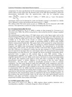
Near-Infrared Single-Photon Detection
231
5 1015202530
10
-6
10
-5
10
-4
10
-3
10
-2
Dark count rate
Detection Efficiency (%)
Afterpulsing Probability
Fig. 4. Dark count rate and afterpulsing probability as a function of detection efficiency
Except rising the temperature, the other method to suppress the afterpulsing effect relies on
decreasing the carriers passing through the APD, where shortening the gating width can
decrease carriers. Figure 5 presents afterpulsing probability as a function of the gating
width. It proves that short gating width is effective to suppress the afterpulsing effect for
high speed operation.
12345
1E-4
1E-3
0.01
0.1
Afterpulsing probability
Gating Width (ns)
Fig. 5. Afterpulsing probability with the electric gating width
2.2 Self-cancellation technique
As mentioned above, shortening the gating width can decrease the number of bulk carriers
passing through the InGaAs/InP APD, so it can weaken the afterpulsing effect for high
speed operation. However, the avalanche current becomes weaker. It requires higher
sensitivity, as well as better capacitive-response cancellation, to catch the avalanche pulse in
the capacitive response. As shown in Fig. 1, the frequency responses between the
InGaAs/InP APD and the variable capacitance are quite different when the frequency > 500
MHz. So, the variable capacitance cannot produce absolutely same capacitive response with
the InGaAs/InP APD, although it has a same value of the capacitance. The self-cancellation
technique solves the problem nicely. Figure 6 is the schematic of this technique. The electric
signal on the cathode of the InGaAs/InP APD is sent to a 50/50 power splitter to produce
Photodiodes - World Activities in 2011
232
two equal components. Then the two identical components are combined by a differencer,
where one of the components is delayed by one gating period. The output of the differencer
is the difference of the two components. Actually, they are the signals of two adjacent gating
periods. The capacitive response is cancelled by itself. As a result, weak avalanche pulse can
be discriminated at high-speed gating rate. (Yuan et al., 2010) promoted the gating rate as
high as 2 GHz with the gating width of only 250 ps.
Fiber
0
o
180
o
Output
Amp
APD
Cooling box
Splitter
Differencer
Delay
Bias
Fig. 6. Schematic of the self-cancellation circuit
2.3 Optical self-cancellation technique
In self-cancellation technique, the electric signal transmits through two coaxial cables. Due
to the large transmission loss of the coaxial cable, the delay of one component cannot be too
long; resulting in the gating rate should be high (e.g. > 200 MHz). Moreover, the electric
circuit of the self-cancellation has a very wide bandwidth > 2 GHz. It should take more
attention on designing and manufacturing for high cancellation ratio of the capacitive
response. The optical self-cancellation technique gives a simple method to realize self-
cancellation in wide bandwidth, including the operation at low gating rate.
Figure 7 is the schematic of the optical self-cancellation. The InGaAs/InP APD response is
magnified by a low-noise broadband amplifier to trigger a DFB laser diode at 1550 nm. The
response bandwidth of the laser diode is 2.5 GHz, fast enough to transfer the electronic
signal to light pulse while keeping the same shape. In this way, the AC electronic signal is
transformed to optical signal, preserving the original information from the InGaAs/InP
APD including the capacitive response and the avalanche pulse. The fiber connecting the
splitter and the detectors has different lengths to introduce a delay of one gating period
between the two components. A fiber stretcher is employed to precisely control the delay
Fiber
Bias
APD
Cooling box
DC Bias
LD
Amp
AMP
Output
PD+
BS
Fiber delay
Fig. 7. Schematic of the optical self-cancellation circuit, where LD is a 1550-nm DFB laser
diode, BS is a 50/50 fiber splitter, PD+ and PD- are the balanced optical detector
Near-Infrared Single-Photon Detection
233
between the two components with 0.17-ps resolution. Two conventional photodiodes are
used to detect the optical signals from each fiber. The response of the photodiodes exactly
replayed the detection signal of the APD. At the output of the balancer, the identical
capacitive response is subtracted. With this optical self-differential photodetector, the weak
avalanche current can be measured (Wu et al., 2009).
3. Photon-number-resolving detection based on a InGaAs/InP APD
It was thought that a single APD cannot resolve the incident photon number without time
or space multiplexing techniques since the gain on the APD is saturated in Geiger mode.
However, recent research result reveals that the avalanche current is proportional to the
photon number of the input light pulse when the APD is operated in non-saturated Geiger
mode. Figure 8 gives a typical avalanche trace. It is recorded by a 6-GHz digital oscilloscope
with the gating width of 5 ns. The current grows gradually first within area (a), and then it
becomes saturated in area (b). Area (a) is the non-saturated Geiger mode period that the
current is proportional to the input photon number. However, the saturation inhibits all the
variation in the early avalanche development in area (b). The avalanche is just beginning in
area (a), which the current is much weaker than the current in area (b). Through the optical
self-cancellation technique, the non-saturated avalanche pulse is observed successfully.
-10123
0.0
0.1
0.2
b
Amplitude (V)
Time (ns)
a
Fig. 8. An avalanche trace in 5-ns electric gate
Figure 9 is a typical histogram of the output peaks of the avalanche pulses. The distribution
of the peak output of the avalanche pulses shows 3 peaks. Obviously, these distribution
peaks are induced by different input photon number. The input light is from a DFB laser.
This coherent light source obeys the Poissonian distribution, where the photon number (n) is
determined by the probability:
(,)
!
n
p
ne
n
−
μ
μ
μ= (1)
where
μ
the is the mean photon number per pulse. The probabilities of the peak output of the
avalanche pulses are calculated according to the Poissonian distribution, which is given by:
Photodiodes - World Activities in 2011
234
0
() (,) (,)
n
PV p n nV
∞
=
=μ⋅ρ
(2)
where
ρ
(n,V) is the distribution of the peak output of the avalanche pulses when they are
induced by n-photon. It shows a Gaussian-like distribution. The calculated data fits well
with the measured data as shown in Fig. 9, proving that the avalanche current in non-
saturated Geiger mode is proportional to the input photon number. The width of n-photon
peak is
√
n (n > 1) scaled to the 1-photon peak, which is caused by the statistical fluctuation.
The width of 1-photon peaks is determined by the avalanche multiplication, and the excess
noise derived from the statistical nature of the avalanche multiplication of the InGaAs/InP
APD.
0.0 0.2 0.4 0.6
n=3
n=2
Probability (a.u.)
Peak voltage (V)
n=1
Fig. 9. Distribution of the peak output of the avalanche pulses, where the black line is the
measured data, the red line is the calculated data. The detected mean photon number is 1.9
per pulse at the detection efficiency of 10%
Figure 10 is the color-grading waveforms of the avalanche pulses in non-saturated Geiger
mode. It is recorded by a 6-GHz digital oscilloscope with the integration time of 0.1 second.
Three peaks of the distribution of the avalanche pulses clearly appear in the waveforms.
They are induced by 1-, 2-, and 3-photon, respectively.
Figure 8 shows that the non-saturated Geiger mode exits in a short period of the early
avalanche development. As a result, in order to observe the capability of the photon-
number-resolving (PNR) of the InGaAs/InP APD, the gating width should < 2 ns. In order
to
figure out the relation between the PNR performance and the avalanche multiplication,
the distributions of the peak output of the avalanche pulses at different detection efficiency
are measured
as shown in Fig. 11. It is hard to resolve the photon number at low detection
efficiency. And the optimal period of the detection efficiency for PNR is from 10% to 20%.
Near-Infrared Single-Photon Detection
235
When the detection efficiency increases to 36%, all the peak output of the avalanche pulses
reach the maximum amplitude of 960 mV, the saturation effect appears obviously and the
peak voltage is independent of the incident photon number more than 2. This sets the upper
boundary for the InGaAs/InP APD to resolve photon numbers.
Fig. 10. Color-grading waveforms of the avalanche pulses
0.00.20.40.6
Peak Voltage(V)
0.0 0.3 0.6 0.9
Peak Voltage(V)
0.0 0.4 0.8 1.2
Peak Voltage (V)
0.0 0.1 0.2 0.3
0.0
0.8
1.6
2.4
Probability (a.u.)
Peak Volta
g
e
(
V
)
Fig. 11. Distribution of peak output of the avalanche pulses at different detection efficiencies
The PNR performance is time resolved with the input laser delay, since the non-saturated
Geiger mode is observed in a short gated mode. Figure 12 shows the photon count rate
varies with the laser pulse delay. The electric gating width is about 1.2 ns, while the effective
detection gating width is about 300 ps. Three delays of the input laser are observed, they are
signed as (a), (b), and (c) in Fig. 12. Figure 13 is the distribution of the peak output of the
avalanche pulses at these three points. Obviously, the PNR performance is similar good at
points (a) and (b). And the PNR performance degrades at point (c). As shown in Fig. 8, the
avalanche multiplication gain increases for about 2 ns until saturated. So, the avalanche
current obtains a larger gain when the photon arrives at the rising edge of the electric gate
than that at the falling edge. Therefore, a large multiplication gain is good for PNR
performance before the InGaAs/InP APD is saturated.
Photodiodes - World Activities in 2011
236
-0.2 0.0 0.2
c
b
Photon Count (a.u.)
Delay (ns)
a
Fig. 12. Photon count rate as a function of the laser pulse delay
0.0 0.2 0.4
Peak voltage (V)
0.0 0.2 0.4
Peak voltage (V)
0.0 0.2 0.4
Probability (a.u.)
Peak voltage (V)
Fig. 13. Distribution of the peak output of the avalanche pulses at points (a), (b), and (c),
respectively, where the detected mean photon numbers are 1.33, 1.35, and 1.32, respectively
4. Near-infrared single-photon detection with frequency up-conversion
The single-photon frequency up-conversion can be considered as the sum-frequency
generation (SFG) process as shown in Fig. 14. Suppose that the pump laser is in the single
longitudinal mode. The solution to the coupled-mode equations for the phase-matched
interaction is
given by (Kumar, 1990):
11 2
22 1
ˆˆ ˆ
( ) (0)cos(| | ) (0)sin(| | ),
ˆˆ ˆ
( ) (0)cos(| | ) (0)sin(| | ),
pp
pp
aL a gE L a gE L
aL a gEL a gEL
=−
=+
(3)
where â
1
and â
2
are annihilation operator for the signal and upconverted fields, respectively,
g denotes the nonlinear coupling coefficient, and L is the length of the nonlinear medium. As
indicated in Eq. (3), a complete quantum conversion occurs from â
1
to â
2
when |gEp|L =
π
/2
is satisfied. The single-photon conversion efficiency can be written as:
2
sin (0.5 / )
p
c
PPη= π⋅
(4)
Near-Infrared Single-Photon Detection
237
where P
p
is the effective pump power, and P
c
is the pump power at unity conversion
efficiency.
The complete quantum conversion demands a large nonlinearity of the nonlinear media
together with a strong pump field. Thus, periodically poled lithium niobate (PPLN) is
usually employed in the single-photon frequency up-conversion since it has a large
nonlinear coefficient (d
eff
=14 pm/V) and provides a large quasi-phase-matching (QPM)
interaction length in the order of 10 mm. The single-photon frequency up-conversion has
been demonstrated in a PPLN waveguide or bulk PPLN. With a PPLN waveguide, the
requirement on the pump field power can be lowered since the power of the optical field
can be confined to a small volume in the waveguide to have a very high intensity. The PPLN
waveguide scheme requires subtle processes to prepare a monolithic fiber pigtailed PPLN
waveguide, which will induce an avoidless big insertion loss (Tanzilli et al., 2002; Langrock
et al., 2004&2005). And the bulk PPLN scheme requires a high pump power, e.g. using a
resonant pump cavity with a stable cavity lock to enhance the circulating pump power
(Albota et al., 2004); or enhancing single-photon frequency up-conversion by intracavity
laser pump (Pan et al., 2006).
Fig. 14. Schematic of single-photon frequency up-conversion
For single-photon frequency up-conversion, one of the key parameters is the signal to noise
ratio. If the noise is much larger than the signal photons, it will be meaningless to take the
trouble to do the up-conversion. Therefore, suppressing the noise will much improve the
performance of the single-photon frequency up-conversion in the applications. Figure 15
shows the possible noise sources in the intracavity enhanced up-conversion system
discussed in the section above. The dark counts from the Si-APD SPD (10~200 counts per
second depending on the device) could be neglected since the dark counts from the
background photons are much larger. The main contribution to the background photons
comes from the strong pump field. The background photons at 808 and 1064 nm comes from
the solid-state laser itself. Besides the up-conversion process with the incident single
photons, other nonlinear effects also takes place in the nonlinear media, such as second
harmonic generation (SHG) of the pump laser at 532 nm and the optical parametric
generation (OPG) fluorescence. These background photons could be removed by the filter
system since they are at different wavelengths from the signal photons. However, among
the background photons, there are some of the same wavelengths with the signal photons at
631 nm. They are caused by up-conversion of the parametric fluorescence caused by the
Photodiodes - World Activities in 2011
238
strong pump field. At first, spontaneous down-conversion of the strong pump took place in
the nonlinear media as ω
1064nm
=ω
1550nm
+ω
3400nm
. In this process, the parametric fluorescence
photons at 1550 nm are of the same wavelength with the incident signal photons. And since
the temperature of the nonlinear media is tuned for the phase matching of SFG for ω
1064nm
+
ω
1550nm
= ω
631nm
, these noise photons are up-converted together with the incident signal
photons with high efficiency. Therefore, some of the output photons at 631 nm are not the
replica of the incident signal photons but the noise from the up-converted parametric
fluorescence. Unfortunately, these background photons can not be removed spectrally by
the filters and contributed a lot to the dark counts on the Si-APD SPD.
Several groups have proposed the long-wavelength pump scheme to overcome the
troublesome up-converted parametric fluorescence (Langrock et al., 2004; Dong et al., 2008;
Kamada et al., 2008). By choosing a comparatively long-wavelength pump, which means the
energy of the pump photons is lower than that of the signal photons, the parametric
fluorescence from the down conversion will not fall in the incident infrared signal photon
spectral regime. As a result, the pump induced parametric fluorescence can be efficiently
suppressed and the dark counts will be greatly lowered. We have demonstrated an efficient
single-photon frequency up-conversion system for the infrared photons at 1064 nm with
ultralow dark counts (Dong et al., 2008). The pump source was provided by a mode-locked
erbium-fiber laser. The repetition rate of the pulse train was 15.8 MHz and the pulse
duration was measured to be 1.4 ps. The average output power of the amplifier was
measured to be 27 mW. The peak power of the pulsed laser was ~220 W, high enough to
achieve unity conversion efficiency in the system. With such a pulsed pump source, no
cavity enhancement was required, much simplifying the whole system. A long-pass filter
with 1000 nm cutting off was placed in front of the PPLN crystal to block the stray light
from the erbium doped fiber amplifier (EDFA), such as the pump for the EDFA from the LD
at 980 nm and the green and red up-conversion emission of the EDFA. In this long-
wavelength pump system, the relatively lower energy pump photon would not induce
undesired parametric fluorescence at the signal wavelength 1550 nm, and the dark counts at
SFG wavelength from followed up-conversion of the parametric fluorescence was
eliminated. Moreover, besides that the Si-APD SPD did not respond to pump light at 1550
nm, the up-conversion fluorescence by the second harmonic of the strong pump was not
phase matched at this working temperature, thus the noise from that process could also be
ignored. Thanks to sufficient suppression of the intrinsic background photons, the narrow
bandpass filter was even not necessary in the filtering system, increasing the transmittance
of the filtering system. After the filtering system, we measured the dark counts of the whole
detection system and got a count rate of ~150 counts per second, when there were neither
signal nor pump photons feeding. Moreover, when there was pump feeding, the dark count
rate was still around 150 counts per second, indicating that the dark counts were not from
the nonlinear parametric processes caused by the strong pump but mainly due to dark
counts of Si-APD SPD and ambient background light. With this system, we achieved so far
the lowest noise to efficiency ratio of ~160 for a near unity conversion efficiency (93%) as
shown in Fig. 16.
The single-photon frequency up-conversion has not only shown a solution to the sensitive
detection of the infrared weak signals but also provided a technique to manipulate quantum
states of the photons. Novel ideas on the techniques for single-photon frequency up-
Near-Infrared Single-Photon Detection
239
conversion come forth from time to time, highlighting its applications in the quantum
information processing.
Fig. 15. Noise of the intracavity single-photon up-conversion
Fig. 16. Schematic of the
long-wavelength pumped frequency up-conversion
5. Few-photon detection with linear external optical gain photodetector
Different from the most methods to amplify the photo-excited carrier with a large internal
electric multiplication gain by electronic devices, we employed the optical devices to
amplify the few-photon before detecting by a conventional PIN photodiode. Interestingly,
the photodiode response showed a linear dependence on the incident photon signals,
promising a novel few-photon detection technique.
Photodiodes - World Activities in 2011
240
Single-photon amplification by stimulated emission becomes the focus of research interest in
recent years due to its application in quantum cloning (Simon et al., 2000; Fasel et al., 2002). In
order to detect the amplified photon signals with conventional PIN photodiodes, the amplifier
should be chosen under the constraint of a high gain. In addition, the amplifier noise due to
the spontaneous emission should be suppressed enough to allow the identification of photons
due to the stimulated emission. Er-doped optical fibers are commonly used in the optical fiber
communication as amplifiers due to their large gain up to 40 dB around 1550 nm. But the
spontaneous emission always accompanies the stimulated emission and will be amplified as
well, which would be the big barrier to identify the signal photons from the noise. In order to
suppress the amplified spontaneous emission (ASE), we separated the amplification into two
steps. Figure 17(a) shows the setup of the external-gain photodetector based on the single-
photon amplification. The light source is a laser diode modulated by an intensity modulator at
25.0 MHz with pulse duration of 325 ps. The output spectrum of the laser is shown by the
green line in Fig. 18(b). The central wavelength is at 1550.20 nm and the full width at half
maximum (FWHM) is 0.02 nm. The output of the laser is attenuated to contain only a few
photons per pulse. Then, the photons are sent to the first EDFA for amplification. In order to
detect the stimulated emission photons, spectral filtering is necessary because the ASE
spectrum of the EDFA covered a broad range from 1527.36 to 1563.84 nm. Firstly, an inline
bandpass filter (IF
1
) centered at 1550 nm with the FWHM of 3 nm is inserted to roughly extract
the amplified signal photons from the broadband fluorescence.
Secondly, the combination of the two fiber Brag gratings (FBG
1, 2
) with the FWHM of 0.18
nm form another bandpass filter. By tuning the temperature to combine the rising edge of
FBG
1
and the falling edge of FBG
2
, a final bandwidth of the bandpass filter was determined
to be 0.06 nm. Finally, a fiber polarization controller (PC) together with a polarization beam
splitter (PBS) helps to remove the ASE noise of the orthogonal polarization. Then, the optical
signal is sent to another EDFA for the amplification again. Since the incident photons are
pre-amplified while most of the ASE noise is removed before the second amplification, the
ASE of the second EDFA itself is much suppressed and instead the stimulated amplification
is enhanced. Spectral filtering is not as strict as in the first step. The filtering system for the
second amplification is composed of a bandpass inline filter (IF
2
) with the FWHM of 3 nm
and a fiber Brag grating FBG
3
with the FWHM of 0.18 nm. The PBS is not even necessary in
the second step because the ASE of the orthogonal polarization in the second EDFA is so
weak that it could be ignored. The black line in Fig. 17(b) shows the ASE spectrum after the
two-step amplification. The spectral width is mainly constrained by the combined FBG
filters in the first step. When the signal photons are sent in, the peak at 1550.20 nm raises on
the top of the ASE spectrum as shown by the red line in Fig. 17(b), indicating the stimulated
amplification of the incident photons. The total gain of the two EDFAs is measured
separately to be about 42.7 dB, indicating that an incident photon could be amplified to ~10
4
photons per pulse (about 1 mW of the peak power) after the two-step amplification. The
optical pulse signal is detected by a PIN photodiode. The variance of the ASE noise is
measured and plotted as a function of the ASE output power as shown in Fig. 17(c). Since
the main voltage noise is derived from the ASE beat on the PIN photodiode, the variance of
the noise increased nonlinearly with the average output power, indicating that the ASE
noise could be considered as a classical noise. The voltage noise amplitude is in Gaussian
distribution with an FWHM of ~140 mV (Fig. 17(d)).
Figure 18 plots the color-grading waveforms of the output voltage measured by the DPX
acquisition mode of a 2.5-GHz oscilloscope with an average incident photon number of μ = 4
Near-Infrared Single-Photon Detection
241
and 16. From the oscilloscope traces, it is observed that the peak output signal amplitude
changes with the incident photon numbers, showing the evidence of the photon number
resolving ability of the detector. The amplitude of the peak output signal shows a linear
dependence on the input average photon number as shown in Fig. 20, indicating that the
EDFAs and the photodiode are far from saturation under such milliwatt optical input power
and capable of registering more than 16 individual photons. By taking into account the optical
amplification, the photodiode response and the electronic amplification, the sensitivity of the
whole setup is obtained by fitting the curve in Fig. 19 to be 15.39 mV/photon.
The photon statistics is studied by analyzing the histograms of the voltage signal acquired
by the oscilloscope. The temporal resolution of oscilloscope is set to 100 ps, and the voltage
amplitude resolution is set to 4 mV. A 500-ps sampling window is used in the analysis.
Figure 20 plots the histograms of the peak output signal voltage recorded for different
incident photon numbers of μ = 4 and 16 per pulse. The red lines in Fig. 21 show a
simulation of the experimental data assuming a Poisson distribution for the incident
photons. Due to the ASE noise variance, the distribution histograms are broadened,
dimming the boundary for different photon numbers. By taking into account the Poisson
distribution of the incident photons, the single photon response of the system is obtained to
be 68 mV by fitting the curves in Fig. 20, and the quantum efficiency of the EDFAs is
calculated to be 22.7%. Due to the linearity of the external-gain photodetector, the curves of
the peak voltage kept the shapes of the ideal Poisson distribution of the input photons. The
probability statistics of the peak output voltage could be also observed in Fig. 18 directly by
its color-grading.
Er
3+
AMP
1
AMP
2
50Ω
PD
FBG
3
Cir
3
IF
2
EDFA
2
EDFA
1
Attn
1
Attn
2
BS
IF
1
Cir
1
Cir
2
FBG
1
FBG
2
PC
PBS
99%
Bias
×10
V
out
×10
Er
3+
LD
Er
3+
Er
3+
AMP
1
AMP
2
50Ω
PD
FBG
3
Cir
3
IF
2
EDFA
2
EDFA
1
Attn
1
Attn
2
BS
IF
1
Cir
1
Cir
2
FBG
1
FBG
2
PC
PBS
99%
Bias
×10
V
out
×10×10
Er
3+
Er
3+
LD
0 102030405060
0.0
1.0
2.0
3.0
4.0
5.0
Variance of the noise (x10
-3
)
Average ASE power (μW)
1550.00 1550.20 1550.40
0.0
2.0
4.0
6.0
8.0
10.0
ASE
Amplified signal
Laser output
Power (
μ
W)
Wavelength (nm)
0.0 0.1 0.2 0.3 0.4
0
1
2
3
4
Experimental data
Simulation
Probability (%)
Peak output signal (V)
140 mV
Fig. 17. (a) Schematic of the external-gain detector, where IF1,2: inline filters, FBG1-3: fiber
Bragg gratings, Cir1-3: fiber circulators, PC: polarization controller, PBS: polarization beam
splitter, PD: conventional pin photodiode, AMP: RF amplifiers. (b) Spectra of the laser
(blue), ASE of the EDFA (green) and amplified single-photon signal (red). (c) variance of the
ASE noise with the ASE power; (d) Distribution of the peak output of one photon.
Photodiodes - World Activities in 2011
242
Due to the lager spontaneous emission of the EDFA, the detector cannot discriminate single-
photon pulses. The FWHM of the bandpass filter is 0.06 nm as well as about 7.4 GHz. The
laser pulse width is ~325 ps, corresponding to the laser bandwidth in the order of 10 GHz.
The filers fits well with the laser pulse, but the insertion loss of the filters is about 15dB,
most of them comes from FBG
1
and FBG
2
. So, more efforts are needed to suppress the
spontaneous emission to decrease the insertion loss. However, the detector can be used as a
sensitive power meter at single-photon lever, as the integral output has a good linearity to
the input photon number, while the noise is averaged.
Fig. 18. Waveforms of the voltage output recorded by the oscilloscope with incident photon
number of (a) 4 and (b) 16.
0 5 10 15
0
75
150
225
300
Average peak amplitude (mV)
Average photon number
0 153045
0.0
1000.0
2000.0
3000.0
4000.0
5000.0
Noise variance (mV
2
)
Average ASE power (μW)
Fig. 19. Peak output voltage of the amplified photon signals and ASE noise variance. (a)
Average peak amplitude as a function of the incident photon number. (b) ASE noise
variance dependent on the output power.
Near-Infrared Single-Photon Detection
243
0.0 0.2 0.4 0.6 0.8
0.00
0.50
1.00
1.50
2.00
2.50
Probability (%)
Peak voltage (V)
0.00.20.40.60.8
0.00
0.03
0.05
0.07
0.10
0.13
Peak voltage (V)
Fig. 20. Distributions of peak output signal for incident pulses of different average photon
numbers, together with the calculated distributions
6. Conclusion
InGaAs/InP APDs are typically operated in gated Geiger mode for near-infrared single-
photon detection. The afterpulsing effect becomes the major obstacle for high speed
detection with the gating rate > 200 MHz, which should use short gating width (e.g. ~1 ns).
The capacitive response of the InGaAs/InP APD must be cancelled to distil the weak
avalanche pulse. We introduce three kinds of capacitive-response cancellation techniques,
where the balanced capacitance cancellation technique is robust for operation at the gating
rate < 200-MHz; and the self-cancellation and optical self-cancellation techniques are
effective in higher gating rate up to 2 GHz. On the other hand, InGaAs/InP APDs are
operated in non-saturated Geiger mode when the gating width < 2 ns. In this mode, the
Photodiodes - World Activities in 2011
244
output of the InGaAs/InP APD is proportional to the input photon number. And we prove
that the PNR performance is determined by the multiplication gain of the InGaAs/InP APD
and input time of the photons.
Optical techniques are potential to realize high performance near-infrared single-photon
detection. One of them is the single-photon frequency up-conversion. The major problem of
up-conversion is the background photons induced by the optical nonlinear process, which
could be resolved by using long-wavelength pump laser, and the background photons are
suppressed at a negligible level. The other optical technique is just starting that detects few-
photon pulse with a conventional linear photodiode after amplified by an external optical
amplifier. Up to now, it still need efforts to realize an ultra-low noise optical amplifier for
few-photon detection.
7. Acknowledgment
This work was funded, in part, by the National Natural Science Fund of China (10904039,
10525416, 10990101, and 91021014), Key Project Sponsored by the National Education
Ministry of China (108058), Research Fund for the Doctoral Program of Higher Education of
China (200802691032), and Shanghai Rising-Star Program (10QA1402100).
8. References
Bennett, C. H. & Brassard, G. (1984). Quantum cryptography: Public key distribution and
coin tossing. Proc. IEEE Int. Conf. Comput. Syst. Signal Process., pp. 175–179
Gisin, N.; Ribordy, G.; Tittel, W. & Zbinden, H. (2002). Quantum cryptography. Rev. Mod.
Phys., Vol.74, pp. 145–195
Knill, E.; Laflamme, R. & Milburn, G. J. (2001). A scheme for efficient quantum computation
with linear optics. Nature Vol.409, pp. 46-52
Stipčević, M.; Skenderović, H. & Gracin, D. (2010). Characterization of a novel avalanche
photodiode for single photon detection in VIS-NIR range. Opt. Express, Vol.18, pp.
17448-17459
Yuan, Z. L.; Kardynal, B. E.; Sharpe, A. W. & A. J. Shields (2007). High speed single photon
detection in the near infrared. Appl. Phys. Lett. Vol.91, 041114
Namekata, N.; Sasamori, S. & Inoue, S. (2006). 800 MHz single-photon detection at 1550-nm
using an InGaAs/InP avalanche photodiode operated with a sine wave gating. Opt.
Express. Vol.14, pp. 10043–10049
Kardynal, B. E.; Yuan, Z. L. & Shields, A. J. (2008). An avalanche-photodiode-based photon-
number-resolving detector. Nature Photonics Vol.2, pp. 425-428
Wu, G.; Jian, Y.; Wu, E; Zeng & H. P. (2009). Photon-number-resolving detection based on
InGaAs/InP avalanche photodiode in the sub-saturated mode. Opt. Express Vol.17,
18782
Yuan, Z. L.; Dynes, J. F.; Sharpe, A. W. & Shields, A. J. (2010). Evolution of locally excited
avalanches in semiconductors. Appl. Phys. Lett. Vol.96, 191107
Takeuchi, S.; Kim, J.; Yamamoto, Y. & Hogue, H. H. (1999). Development of a high-
quantum-efficiency single-photon counting system. Appl. Phys. Lett. Vol.74, pp.
1063-1065
Near-Infrared Single-Photon Detection
245
Miller, A. J.; Nam, S. W.; Martinis, J. M. & Sergienko, A. V. (2003). Demonstration of a low-
noise near-infrared photon counter with multiphoton discrimination. Appl. Phys.
Lett. Vol.83, pp. 791-793
Schuster, D. I.; Houck, A.; Schreier, J.; Wallraff, A.; Gambetta, J. M.; Blais, A.; Frunzio, L.;
Majer, J.; Johnson, B.; Devoret, M. H.; Girvin, S. M. & Schoelkopf, R. J. (2007).
Resolving photon number states in a superconducting circuit. Nature Vol.445, pp.
515-518
Shields, A. J.; O’Sullivan, M. P.; Farrer, I.; Ritchie, D. A.; Hogg, R. A.; Leadbeater, M. L.;
Norman, C. E. & Pepper, M. (2000). Detection of single photons using a field-
effect transistor gated by a layer of quantum dots. Appl. Phys. Lett. Vol.76, pp.
3673-3675
Albota, M. A. & Wong, F. N. C. (2004). Efficient single-photon counting at 1.55 μm by means
of frequency upconversion. Opt. Lett. Vol.29, 1449
Pan, H. F.; Dong, H. F. & Zeng, H. P. (2006). Efficient single-photon counting at 1.55 mm by
intracavity frequency upconversion in a unidirectional ring laser. Appl. Phys. Lett.
Vol.89, 191108
Thew, R. T.; Tanzilli, S.; Krainer, L.; Zeller, S. C.; Rochas, A.; Rech, I.; Cova, S.; Zbinden, H. &
Gisin, N. (2006). Low jitter up-conversion detectors for telecom wavelength GHz
QKD. New J. Phys. Vol.8, 32
Han, X. F.; Weng, Y. X.; Wang, R. Chen, X. H.; Luo, K. H.; Wu, L. A. & Zhao, J. M. (2008).
Single-photon level ultrafast all-optical switching. Appl. Phys. Lett. Vol.92,
151109
Wu, G.; Jian, Y.; Wu, E & Zeng, H. P. (2010). Linear external optical gain photodetector at
few-photon level. IEEE Photon. Tech. Lett. Vol.22, pp. 688-690
Wu, G.; Zhou, C. Y.; Chen, X. L. & Zeng, H. P. (2006). High performance of gated-mode
single-photon detector at 1.55 µm. Opt. Comm. Vol.265, pp. 126-131
Itzler, M. A.; Ben-Michael, R.; Hsu, C. F.; Slomkowski, K.; Tosi, A.; Cova, S.; Zappa, F. &
Ispasoiu, R. (2007). Single photon avalanche diodes (SPADs) for 1.5 μm photon
counting applications. J. Mod. Opt. Vol.54, pp. 283–304
Bethune, D. S. & Risk, W. P. (2000). An autocompensating fiber-optic quantum
cryptography system based on polarization splitting of light. IEEE J. Quantum
Eletron. Vol.36, pp. 340-347
Tomita, A. & Nakamura, K. (2002). Balanced, gated-mode photon detector for quantum-bit
discrimination at 1550 nm. Opt. Lett. Vol.27, pp. 1827-1829
Liang, Y.; Jian, Y.; Chen, X. L.; Wu, G.; Wu, E & Zeng, H. P. (2011). Room-temperature
single-photon detector based on InGaAs/InP avalanche photodiode with
multichannel counting ability. IEEE Photon. Tech. Lett. Vol.23, pp. 115 – 117
Yuan, Z. L.; Sharpe, A. W.; Dynes, J. F.; Dixon, A. R. & Shields. A. J. (2010). Multi-gigahertz
operation of photon counting InGaAs avalanche photodiodes. Appl. Phys. Lett.
Vol.96, 071101
Kumar P. (1990). Quantum frequency conversion. Opt. Lett. Vol.15, pp. 1476-1478
Tanzilli, S.; Tittel, W.; De Riedmatten, H.; Zbinden, H.; Baldi, P.; De Micheli, M.; Ostrowsky,
D. B. & Gisin, N. (2002). PPLN waveguide for quantum communication. Eur. Phys.
J. D Vol.18, pp. 155-160
Photodiodes - World Activities in 2011
246
Langrock, C.; Diamanti, E.; Roussev, R. V.; Yamamoto, Y.; Fejer, M. M. & Takesue, H. (2004).
Periodically poled lithium niobate waveguide sum-frequency generator for
efficient single-photon detection at communication wavelengths. Opt. Lett. Vol.29,
pp. 1518-1520
Langrock, C.; Diamanti, E.; Roussev, R. V.; Yamamoto, Y.; Fejer, M. M. & Takesue, H. (2005).
Highly efficient single-photon detection at communication wavelengths by use of
upconversion in reverse-proton-exchanged periodically poled LiNbO3
waveguides. Opt. Lett. Vol.30, pp. 1725-1727
Dong‚ H. F.; Pan‚ H. F.; Li‚ Y.; Wu E & Zeng, H. P. (2008). Efficient single-photon frequency
upconversion at 1.06 μm with ultralow background counts. Appl. Phys. Lett. Vol.93‚
071101
Kamada, H.; Asobe, M.; Honjo, T.; Takesue, H.; Tokura, Y.; Nishida, Y.; Tadanaga, O. &
Miyazawa H. (2008). Efficient and low-noise single-photon detection in 1550 nm
communication band by frequency upconversion in periodically poled LiNbO3
waveguides. Opt. Lett. Vol.33, pp. 639-641
Simon, C.; Weihs, G. & Zeilinger, A. (2000). Optimal quantum cloning via stimulated
emission. Phys. Rev. Lett. Vol.84, pp. 2993-2996
Fasel, S.; Gisin, N.; Ribordy, G.; Scarani, V. & Zbinden, H. (2002). Quantum cloning with an
optical fiber amplifier. Phys. Rev. Lett. Vol.89, 107901 (2002)
11
Geiger Avalanche Photodiodes (G-APDs)
and Their Characterization
Giovanni Bonanno, Massimiliano Belluso,
Sergio Billotta, Paolo Finocchiaro
and Alfio Pappalardo
INAF - Osservatorio Astrofisico di Catania,
INFN – Laboratori Nazionali del Sud Catania
Italy
1. Introduction
In many fields and in particular in astrophysical observations, a chronic problem is the
photon-starving condition, which becomes severe when images are to be obtained in short
acquisition times (from micro to milliseconds), as happens in hot areas of astrophysics:
optical counterparts of high-energy gamma-ray bursts, study and interpretation of
Supernovae bursts. CCDs are inherently unable to provide accurate measurements of such
fast low-intensity transients at high frame rates. To respond to single photons, suitable
detectors must provide output signals that are sufficiently high to be individually processed
by electronic circuits. Therefore, only detectors with an internal mechanism that provides a
high multiplication of charge carriers are suitable, namely vacuum tube photomultipliers
(PMTs), solid-state avalanche photodiodes (APDs) and electron-multiplying CCDs (EM-
CCDs). In PMTs, the photocathodes available for the visible spectral range provide fairly
good quantum efficiency and low noise, whereas cathodes for the red and near-infrared
range have lower quantum efficiency and must be cooled to reduce the dark-count rate.
PMTs are bulky, and so not suitable for assembly in large arrays, fragile, sensitive to
electromagnetic disturbances and mechanical vibrations, require high supply voltages (1–2
kV) and are costly devices, particularly the high-performance models. EM-CCDs exploit an
internal multiplication process to achieve sub-electron readout noise, thus being able to
detect single photons. Their quantum efficiency is very high, and they are inherently suited
to imaging applications. However, due to their readout technique, they cannot provide
frame rates higher than a few kilo-frames per second, and cannot be used in extreme time-
resolved measurements. Single photons can be detected efficiently by avalanche diodes
operating in Geiger mode, known as Single-Photon Avalanche Diodes (SPADs). Avalanche
photodiodes have the typical advantages of solid state devices (small size, low bias voltage,
low power consumption, ruggedness and reliability, suited to building integrated systems).
In the last few years, a new kind of planar semiconductor device has slowly but steadily
come out, namely the silicon photomultiplier (SiPM), with promising features that, in some
respect, could even replace traditional photomultiplier tubes (Kovaltchouk et al, 2005).
Based on a Geiger mode avalanche photodiode elementary cell, it consists of an array of n
Photodiodes - World Activities in 2011
248
independent identical microcells whose outputs are connected together. The final output is
thus the analog superposition of n ideally binary signals (Buzhan et al., 2003). This scheme,
along with the sensitivity of each individual cell to single photons, appears to result, in
principle, in the perfect photo-sensor capable of detecting and counting single photons in a
light pulse. Unfortunately, this is not the case, considering that this kind of device has
several drawbacks and all of them are mainly derived from its noise features; due to lattice
defects and impurities in the basic material, the dark counts cannot be reduced below a
given rate, and as these mainly have a thermal origin, one could be tempted to solve the
problem by cooling the device itself. This works to a given extent; however, another
problem sets in, namely afterpulsing, due to charge carriers trapped within the
semiconductor during the avalanche signal and later exponentially released. Cooling the
device results in an increase of the exponential decay constant, and therefore, the lowest
operating temperature becomes a tradeoff between random thermal counts and long-lasting
afterpulse counts (Ghioni et al., 1996). This could represent an intrinsic limitation to the
implementation of large-area G-APD detectors, if one actually needs the single photon
sensitivity. Nonetheless, the suitable use of G-APDs depends strongly on a particular
application; although dark counts are a problem for low-level light applications, if there is
ample light, one can set the threshold at several photoelectrons and thus suppress them.
Such a tradeoff can be useful to optimize the energy resolution. Therefore, although not
capable of totally replacing the traditional photomultiplier tubes, the SiPM already promises
to fulfill a wide set of requirements coming from numerous applications. Thanks to its
properties, the multi-element G-APD is currently promising to find widespread use in
nuclear medical imaging applications like Positron Emission Tomography (PET). In this
application the G-APD is usually coupled to Lutetium Orthosilicate (LSO) or Lutetium-
Yttrium Orthosilicate (LYSO) scintillators which convert gamma-rays into optical photons in
the blue and in the near ultraviolet wavelength ranges
(Melcher, 1992).
In this chapter, we describe the single and multi-element avalanche photodiode operating in
Geiger mode. Their characterization in terms of noise and Photon-Detection Efficiency
(PDE) is treated in great detail together with the adopted experimental setups, partly based
on optical systems i.e. light sources, filters, monochromator and integrating spheres, and
partly based on typical particle counting equipments. The developed technique to obtain
very accurate PDE measurements based on single photon counting with subtraction of dark
noise, and avoiding as much as possible the noise contribution due to cross-talk and
afterpulses is here detailed, as well as the apparatus used for charge signal measurements
based on a pulsed laser system, a charge-to-digital converter (QDC) and a time-to-digital
converter (TDC). Some measurements and results on various single element G-APDs and
multi-element G-APDs, manufactured by different companies, are also discussed. Finally
the two most known methods (photocurrent and photon counting) to evaluate the PDE are
compared and a discussion on how the noise due to afterpulse and optical cross-talk may
influence the measurements is also given.
2. Single element G-APD
A single element G-APD, also called Single Photon Avalanche Diode (SPAD) is essentially a
p–n junction biased at a voltage above the breakdown. At this bias, the electric field is so
high (higher than 3 × 10
5
V/cm) that a single charge carrier injected in the depletion layer
Geiger Avalanche Photodiodes (G-APDs) and Their Characterization
249
can trigger a self-sustaining avalanche and the output current rises (sub-nanosecond rise-
time) to a level of milliamps. If the primary carrier is photo-generated, the leading edge of
the avalanche pulse marks (with picoseconds jitter) the arrival time of the detected photon.
The current continues to flow until the avalanche is quenched by lowering the bias voltage
to or below the breakdown level: the lower electric field is no longer able to accelerate the
carriers to impact-ionize with lattice atoms. Then the bias voltage must be restored, in order
to be able to detect another photon. The circuit that performs such operations is usually
referred to as a quenching circuit (Cova et al., 1996). This operation requires suitable
electronics, able to:
1. sense the leading edge of the avalanche current;
2. generate a standard output pulse, synchronous with the onset of current;
3. quench the avalanche by lowering the bias below the breakdown voltage;
4. restore the photodiode voltage to the operative level.
The most commonly used circuit in studies on Geiger-mode avalanche photodiodes is the
passive-quenching circuit: the avalanche current quenches itself simply by developing a
voltage drop across a high-impedance load (RL > 100 kΩ). Such a circuit is very simple and
can easily be employed, but sets severe limitations on the maximum admissible photon
counting rate and on detector performance in general (Cova et al., 1996). In fact, it was the
introduction of the active-quenching circuit (AQC) concept by S. Cova (Cova et al., 1981)
that opened the way to practical application of SPADs. Many AQC types have since been
reported, with circuit structure and mounting that evolved from standard NIM cards
(Brown et al., 1987) to small SMT boards suitable for compact detector modules (Ghioni et
al., 1996). But, if some limitation on photon counting rate and on timing response is accepted
then, by using quenching resistors, many SPADs can be easily integrated in one chip and a
so called multi-element G-APD can be manufactured with sensitive areas comparable to
those of small photomultiplier tubes.
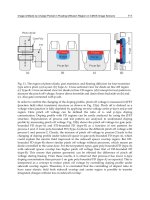
A schematic diagram of the AQC developed at INAF Catania Astrophysical Observatory
Laboratory for Detectors (Billotta et al., 2009) is shown in Fig. 1. The G-APD is reverse
biased through the cathode at V
break
+ V
ex
, where V
break
is a voltage slightly lower than the
Fig. 1. The single element G-APD is biased and driven by an active quenching circuit (AQC),
designed and realized at the INAF Catania Astrophysical Observatory Laboratory for
Detectors (COLD), that provides for extinguishing the avalanche, bringing the SPAD to its
waiting conditions and after a changeable hold-off time making the SPAD ready to detect
another photon.
Photodiodes - World Activities in 2011
250
breakdown and V
ex
brings the total reverse bias over breakdown. When an avalanche is
triggered, the current flowing on Rs activates the discriminator A, which varies the state of
node 2, giving a pulse synchronized with the avalanche. A buffer provides for the output of
the pulse. Two feedback loops are used, one to quench immediately the diode to reduce the
charge trapping and then avoiding afterpulses, and the other to delay the system reset,
keeping quenched the diode for a dead time T known as the hold-off time. The first
feedback loop acts on S
1
switch forcing the diode anode at V
ex
voltage, giving as the total
voltage V
break
and thus leaving the diode quenched. The hold-off time is user selectable.
After the time T the discriminator B by means of the switch SL
1
forces the node 1 at ground,
making the SPAD ready for a new detection. At the same time the discriminators A and B
open S
1
and switch SL
1
to V
ex
.
A sketch of a single SPAD with integrated passive quenching resistor, manufactured by ST
Microelectronics and tested at our laboratory, is shown in Fig. 2. The voltage can be applied
through the pads 1 and 3 or through the pads 2 and 3 in order to, respectively, include or
exclude the quenching resistor R
L
.
In Fig. 3 is shown the reverse characteristic at room temperature obtained biasing the device
including (curve a) and excluding (curve b) the quenching resistor. Measured current above
the BV in curve (a) is lower due to the quenching of the dark events.
Fig. 2. Sketch of a single SPAD with integrated quenching resistor. The voltage is applied
through pads 1–3 to include, or 2–3 to exclude, the quenching resistor R
L
.
The plots of Fig. 3 show that the breakdown voltage is about 29.5 V, while the leakage
current is few picoamps. The low value of the leakage current indicates a low generation of
electrical carriers and then can be considered the first evidence of low defects of this
particular kind of G-APD (Mazzillo et al.).
In order to work as a photodetector, a diode must be able to remain biased above the
breakdown voltage for a sufficient time, of the order of a few milliseconds. This means that
the generation–recombination phenomenon, which would trigger the avalanche, must be
kept very low. Since thermally generated carriers can trigger an avalanche, it is possible to
observe output current pulses also when a SPAD is kept in the dark: such an average
counting rate is called dark-count rate and is one of the key parameters in defining detector
noise (Ghioni et al., 1991). This aspect, as can be seen subsequently, becomes critical in
multi-element G-APDs. The relevant characteristics of SPAD detectors are:
dimensions ranging from 20 µm to 200 µm;
dark count rates that, depending on working temperature, overvoltage and element
dimensions, may vary from 20 counts/s to 1000 counts/s;
Geiger Avalanche Photodiodes (G-APDs) and Their Characterization
251
photon detection efficiency (PDE), determined by the quantum efficiency (QE) and the
trigger probability (TP), that can reach values around 60 % in the visible band.
To understand how the single element G-APD characteristics strongly depend on the bias
voltage, or better, on the over voltage OV, the dark noise and the PDE are here considered.
In Fig. 4 the dark noise rate of a typical device is represented as a function of OV values.
Fig. 3. SPAD reverse I–V characteristics around the breakdown voltage. (a) The quenching
resistor was included. (b) The quenching resistor was excluded.
Fig. 4. SPAD dark noise rate at room temperature and increasing overvoltage.
These measurements were done at room temperature. As can be seen in Fig. 4, the dark
noise rate increases almost linearly with OV. This evidence suggests that afterpulsing effects
are not quite relevant also when high OV is applied to the device. In fact if afterpulsing were
dominant the dark noise rate would grow steeper than linearly. Fig. 5 shows QDE (PDE
with 100% of trigger probability) in the 350 ÷ 900 nm spectral range for a typical device as a
function of the OV.
Photodiodes - World Activities in 2011
252
Both QDE curves show the same shape and reach the maximum at wavelengths between
400 and 500 nm. At 450 nm and 10 % of overvoltage we found a QDE of 30% and a QDE of
17% at 5% of overvoltage. This behavior is strictly related with the triggering probability
that increases with the OV. Both QDE curves show also that biasing the device with these
values, the Geiger efficiency is far from being near its maximum value, in fact the QDE
scales almost linearly with the overvoltage. This means that the best operating condition
will be a tradeoff between the acceptable dark count rate (that can be lowered by cooling the
device) and the PDE, that of course, is preferred as high as possible. In Fig. 6 are plotted
PDE values obtained from characterization of this kind of devices operated at the best
condition of OV and temperature, carried out at the INAF - Catania Astrophysical
Observatory (Billotta et al., 2009).
Fig. 5. SPAD quantum detection efficiency at room temperature and increasing overvoltage.
Fig. 6. (Left) PDE of a STMicroelectronics 40 µm device biased at 20% overvoltage; we can
note the peak of about 60% at 600 nm. (Right) PDE of a MPD 100 µm SPADs. This device
shows a PDE peak of about 60% at 550 nm.
3. Array of single element G-APD
There are applications that may require arrays of single element G-APDs. For instance, one
of the toughest problems affecting ground-based telescopes is the presence of the
Geiger Avalanche Photodiodes (G-APDs) and Their Characterization
253
atmosphere, which distorts the spherical wavefront, creating phase errors in the image-
forming ray paths. Even at the best sites, ground-based telescopes observing at visible
wavelengths cannot achieve an angular resolution in the visible better than telescopes of 10
to 20 cm diameter, because of atmospheric turbulence alone. Adaptive optics is the answer
to this problem: a deformable mirror is inserted in the light path of the telescope, and its
control signal is based on measurement of the incoming wavefront, performed by a suitable
high-sensitivity detector. Single element G-APD arrays can be used as curvature wavefront
sensors (CWFS). By using a pulsed laser system, the array performs better than a CCD,
thanks to its gating function and parallel readout, which allow faster loop cycles (Zappa et
al., 2007). In Fig. 7 is shown a drawing of a planar array fabricated by STMicroelectronics
(Mazzillo et al., 2007). This is manufactured by the integration of 25 pixels with a square
geometry of 5 × 5.
Fig. 7. Plan view of an array fabricated by STMicroelectronics. This device is manufactured
by the integration of 25 pixels with a square geometry of 5 × 5.
STMicroelectronics has designed arrays with three different pixel diameters: 20, 40 and 60
mm. Separation distances between adjacent pixels are in the range of 160 and 240 mm
according to different diameters. Anode contacts are in common for each row, while each
cathode is separately contacted and available from outside by different pads. The typical
breakdown voltage is about 30 V.
4. Multi-element G-APD
Multi-element G-APDs also known as silicon photomultipliers (SiPMs) or multi-pixel
photon counters (MPPCs), have been developed during recent years as a possible alternative
to vacuum photomultiplier tubes (PMT) and avalanche photodiodes (APD). A multi-
element G-APD, is a photodetector constituted by hundreds to thousands of single G-APD,
and the discharge is quenched by a small transparent polysilicon resistor (passive
quenching) integrated on each cell’s cathode. The independently operating cells are
connected to the same readout line and therefore the combined output signal corresponds to
the sum of all fired pixels. A schematic diagram is shown in Fig. 8.
A typical G-APD reaches an intrinsic gain for a single photoelectron of 10
6
, comparable to
that of vacuum phototubes (PMTs). Fig. 9 shows a G-APD of a 10 × 10 array manufactured
by STMicroelectronics.
A snapshot of persistence plots taken on a digital scope is shown in Fig. 10, where the
(upper plot) low-light-level pulses, generated by a laser, produce the typical equally spaced
Photodiodes - World Activities in 2011
254
electrical signals corresponding to discrete numbers of photons detected. The signal rise
time is below 2 ns; its duration is 10 ns. The dark-count signals, shown on the lower plot,
basically show up as one-cell pulses.
Fig. 8. Electrical schematic of the SiPM, its biasing circuit, and output signal extraction.
Fig. 9. Microphotograph of the 10 × 10 SiPM with 50 µm pitch. Each cell’s active area, 30 µm
wide, appears in the picture as a light transparent polysilicon resistor frame surrounding a
darker central spot.
Fig. 10. Persistence plots on a digital scope of a 10 × 10 cells G-APD output signal. The upper
plots is obtained by illuminating the detector with low-light-level pulses generated by a
laser. The equally spaced signals correspond to discrete numbers of photons detected. The
lower plot basically shows as the dark counts are due to one-cell pulse.
Geiger Avalanche Photodiodes (G-APDs) and Their Characterization
255
In multi-element G-APDs the dead area due to the quenching resistor introduces another
parameter that is named “fill factor”. This parameter is responsible of the lower PDE as
compared to that of the single element. Indeed, as it is better explained in section 9, the PDE
is the product of three factors: the quantum efficiency (QE), the trigger probability (TP) and
the fill factor (FF). The electro-optical characteristics of these devices are detailed in the
following sections.
5. Characterised detectors
The characterisation activity described here regards two kinds of G-APD operating in
photon counting regime: SiPMs manufactured by STMicroelectronics and MPPCs
manufactured by Hamamatsu. These G–APDs are biased slightly above the breakdown by
an overvoltage (around 10% for the STMicroelectronics and few percents for the
Hamamatsu). The passive quenching resistor is integrated on the cathode for the
STMicroelectronics and on the anode for the Hamamatsu. In particular here we present the
characterisation results for three G-APDs:
1. a 10 × 10 single elements (100 cells) STMicroelectronics SiPM;
2. a 10 × 10 single elements (100 cells) Hamamatsu MPPC (S10362-11-100C);
3. a 20 × 20 single elements (400 cells) Hamamatsu MPPC (S10362-11-050C).
The detectors have the following geometric characteristics:
the 100-cells SiPM manufactured by STMicroelectronics has dimensions of 0.5 × 0.5 mm
2
, a
pitch of 50µm and a fill factor of 36 %;
the 100-cells MPPC Hamamatsu has dimensions of 1 × 1 mm
2
, a pitch of 100µm and a fill
factor of 78.5%;
the 400-cells MPPC Hamamatsu has dimensions of 1 × 1 mm
2
, a pitch of 50 µm and a fill
factor of 61.5 %;
and the following electrical characteristics:
the STMicroelectronics SiPM has a breakdown voltage around 29.5 Volts at room
temperature, with a variation coefficient of 35 mV/°C;
both Hamamatsu MPPCs have a breakdown voltage around 68.6 V at room temperature.
The 100-cells MPPC has a gain G=2.4 × 10
6
(at a Bias Voltage = 69.7 V), the 400-cells has a
G=7.1× 10
5
(at a Bias Voltage = 69.8 V).
Furthermore we have to note that, on the contrary of Hamamatsu MPPC, each
STMicroelectronics SiPM cell is surrounded by a suitable trench filled with opaque material
to avoid that photons produced during the Geiger discharge may be detected by
neighboring cells. This effect is commonly named as “optical cross-talk” (Dolgoshein, 2006).
6. Experimental setups for multi-element G-APDs electro-optical parameters
measurements
As written in the previous section, in this chapter we report on a complete characterisation
of three different G-APDs. The purpose is to explain how accurate measurements of the
relevant electro-optical parameters can be carried out to better qualify the detector
performances. We measured the following characteristics:
dark counts, afterpulse and optical cross-talk that represent the noise sources;
charge response and gain;
photon detection efficiency (PDE).
To evaluate the above characteristics four different setups are used: