Advanced Radio Frequency Identification Design and Applications Part 6 potx
Bạn đang xem bản rút gọn của tài liệu. Xem và tải ngay bản đầy đủ của tài liệu tại đây (1.45 MB, 20 trang )
Design of a Very Small Antenna for Metal-Proximity Applications
89
The δ values are shown in Fig. 3.12. Here, a copper wire is considered, and the σ value is set
to 5.8 × 10
7
[1/Ωm]. The t value should be more than four times the
δ
value. The calculated
results, i.e., the results obtained using Eq. (3.19), are shown in Fig. 3.13; an important point
to be noted is that the values of R
l
are not sufficiently small. By substituting the L
0
value
determined from Fig. 3.3 in Eq. (3.19), we can calculate the R
l
values for NMHAs. In Fig. 3.3,
L
0
is about 0.48 m (0.95 × 0.5) at 315 MHz, and hence, R
l
is approximately 0.7 Ω. If the
frequency changes and L and d are changed analogously, R
l
becomes inversely proportional
to √λ. The most effective way to reduce R
l
is to increase W or d.
0
1
2
3
4
5
6
7
0.1 1 10
Frequency [GHz]
δ [μm]
Fig. 3.12 Skin depth (δ)
0.1 1 1
0
0.1
1
10
f [GHz]
L =1000 mm
R
l
[Ω]
L =500 mm
L =100 mm
W =1 mm
Fig. 3.13 Ohmic resistance
Advanced Radio Frequency Identification Design and Applications
90
3.2.5 Input resistances
The simulated input resistances (R
in
) of the self-resonant structures are shown in Fig. 3.14.
Here, R
in
is expressed as follows:
R
in
= R
r
+ R
l
=R
rD
+ R
rL
+ R
l
(3.20)
For an R
l
value of approximately 0.7 Ω, R
l
.shares the dominant part of R
in
at H = 0.02 m in
Fig. 3.14 In these small antennas, most of the input power is dissipated as ohmic resistance,
and only a small component of the input power is used for radiation.
0.02 0.04 0.06 0.08 0.10
0.005
0.010
0.015
0.020
0.025
0.030
0.035
D [m]
H [m]
0.84
2.21
4.50
0.92
2.32
4.68
1.00
2.44
4.81
N = 15
N = 10
N = 5
R [Ω]
Fig. 3.14 Input resistances
Table 3.2 gives the details of the input resistances. The calculated results, i.e., the results
obtained using Eqs. (3.2), (3.4), and (3.17), are compared with the simulated results. The
R
rD
+R
rL
values determined from the aforementioned equations agree well with the
simulated results. The calculated and simulated R
l
values also agree well with each other; in
the equation, an α value of 0.6 is used. Finally, the R
in
values are compared, and the antenna
efficiencies (η = (R
rD
+R
rL
)/R
in
) are obtained. The calculated and simulated results agree well,
and thus, the equations are confirmed to be accurate. Moreover, R
l
has a large negative
effect on the antenna efficiency.
Structure R
rD
[Ω] R
rL
[Ω] R
l
[Ω] R
in
[Ω] η[dB]
Eq. 0.0790 0.2378 0.6380 0.9548 -4.7911
N = 5
H = 0.02λ
Sim. 0.2537 0.5862 0.8399 -5.1988
Eq. 0.0790 0.0656 0.8008 0.9453 -8.1554
N = 15
H = 0.02λ
Sim. 0.1987 0.7988 0.9975 -7.0067
Table 3.2 Resistances determined by calculation and simulation
Design of a Very Small Antenna for Metal-Proximity Applications
91
3.2.6 Q factor
The Q factor is important for estimating the antenna bandwidth. The radiation Q factor (Q
R
)
for electrically small antennas is defined as
Q
R
= stored energy (E
sto
)/radiating energy (E
dis
) (3.21)
For antennas, these energies are expressed by the input impedance:
E
sto
= X I
2
(3.22)
E
dis
= R
r
(3.23)
Therefore, Q
imp
can be expressed as follows:
Q
imp
= X/R
r
(3.24)
Another expression for the Q factor is based on the frequency characteristics; in this case, the
Q factor is referred to as Q
A
:
Q
A
= f
c
/
Δ
f (3.25)
Here, f
c
is the center frequency and
Δ
f is the bandwidth. In this expression, a small Q
A
value
indicates a large bandwidth.
McLean [13] gave the lower bound for the Q factor (Q
M
):
3
11
()
M
Q
ka
ka
=+ (3.26)
Figure 3.15 shows examples of Q
A
and Q
M
for NMHAs; Ds is the diameter of the sphere
enclosing an NMHA. The antenna structures labeled A and B are those shown in Fig. 3.16.
The Q
A
values of A and B are based on the measured voltage standing wave ratio (VSWR)
characteristics shown in Fig. 3.19. We can see that Q
A
is smaller than Q
M
, because of the
ohmic resistance of the antenna.
0.015 0.020 0.025 0.030 0.035
1000
10000
A/
λ
Q
M
A
A
B
Q
A
D
A
/λ
Fig. 3.15 Q factors for NMHA
Advanced Radio Frequency Identification Design and Applications
92
3.3 Achieving a high antenna gain
The efficiency (
η
) of a small antenna is defined as
η = (R
rD
+ R
rL
)/(R
rD
+ R
rL
+R
l
) (3.27)
Since (see Table 3.2) R
l
is greater than R
r
(=R
rD
+ R
rL
,), R
l
must be decreased in order to
achieve high antenna efficiency. From Eq. (3.19), it is clear that increasing the antenna wire
width (W) or diameter (d) is the most effective way to reduce R
l
. If W is increased, it would
be necessary to ensure that neighboring wires are well separated from each other.
By substituting Eqs. (3.2), (3.4), and (3.19) in Eq. (3.27), we can calculate
η
; the result is
shown in Fig. 3.16.
It can be seen that
η
decreases with a decrease in H and D. In this case, we use a very narrow
antenna wire (d = 0.05 mm). At points A and B,
η
is 10% (-10 dB) and 25% (-6 dB),
respectively. The relationship between the antenna gain (G
A
) and η is given by
G
A
= G
D
η [dBi] (3.28)
Here, G
D
is the directional gain of the antenna. In electrically small antennas, G
D
remains
almost constant at 1.8 dBi. The antenna gains at points B and A are G
A
= -4.2 dBi and -8.2
dBi, respectively. Given the small antenna size, these gains are large. Moreover, the gains
can be increased if a thicker wire is used. In conclusion, it is possible to achieve a high gain
when using small antennas.
0.005 0.010 0.015 0.020 0.025 0.030
0.005
0.010
0.015
0.020
0.025
0.030
D
A
/
λ
H
A
/
λ
η = 40%
N=5
N=7
N=11
η = 30%
η = 20%
η = 10%
d = 0.55 mm
A
B
Fig. 3.16 Efficiency of NMHA
3.4 Examples of electrical performance
In order to investigate the realistic characteristics, we fabricated a 0.02λ antenna (point B in
Fig. 3.16), as shown in Fig. 3.17. The antenna impedances are measured with and without a
Design of a Very Small Antenna for Metal-Proximity Applications
93
tap feed. The tap structure is designed according to the procedure given in Section 4.2.4.
Excitation is achieved with the help of a coaxial cable. The coaxial cable is covered with a
Sperrtopf balun to suppress the leak current. The measured and calculated impedances are
shown in Fig. 3.18. The results agree well both with and without the tap feed, thereby
confirming that the measurement method is accurate. The tap feed helps in bringing about
an effective increase in the antenna input resistance. The bandwidth characteristics are
shown in Fig. 3.19; the measured and simulated results agree well. The bandwidth at
VSWR < 2 is estimated to be 0.095%.
20.0 mm
19.3 mm
16.0 mm
38.0 mm
Sperrtopf balun
(a) w/o tap (a) With tap
Tap
Fig. 3.17 Fabricated antenna (H = 0.021λ, D = 0.020λ)
10 25 50 100 250
-10j
10j
-25j
25j
-50j
50j
-100j
100j
-250j
250j
Simu
Meas
w/o tap
With tap
315 MHz
Fig. 3.18 Antenna input impedance
Advanced Radio Frequency Identification Design and Applications
94
314.6 314.8 315.0 315.2 315.4
1.0
1.5
2.0
2.5
3.0
VSWR
Frequency [MHz]
0.30 MHz
0.30 MHz
Simu
Meas
Fig. 3.19 VSWR characteristics
-30
-25
-20
-15
-10
-5
0
30
60
90
120
150
180
210
240
27
0
300
330
-30
-25
-20
-15
-10
-5
E
θ
=-5.6 dBi
E
φ
= -8.5 dBi
E
φ
= -8.2 dBi
E
θ
=-5.3 dBi
Sim. Meas.
Fig. 3.20 Radiation patterns
As can be seen from Fig. 3.20, the measured and simulated radiation characteristics are in
good agreement. The E
θ
component corresponds to the radiation from the electric current
Design of a Very Small Antenna for Metal-Proximity Applications
95
source shown in Fig. 3.1, and the E
φ
component corresponds to the radiation from the
magnetic current source shown in Fig. 3.1. There is a 90° phase difference between the E
θ
and E
φ
components. Therefore, the radiated electric field is elliptically polarized. Because the
magnitude difference between the E
θ
and E
φ
components is only 3 dB, the radiation field is
approximately circularly polarized. The magnitude of the E
θ
and E
φ
components correspond
to R
rD
in Eq. (3.2) and R
rL
in Eq. (3.4). The antenna gains of the E
θ
and E
φ
components can be
estimated by the η value shown in Fig. 3.16. The value η × G
D
(G
D
indicates the directional
gain of 1.5) of structure B becomes -4 dBi. This value agrees well with the total power of the
E
θ
and E
φ
components.
4. NMHA impedance-matching methods
4.1 Comparison of impedance-matching methods
For the self-resonant structures of very small NMHAs, effective impedance-matching
methods are necessary because the input resistances are small. There are three well-known
impedance-matching methods: the circuit method, the displaced feed method, and the tap
feed method as shown in Fig. 4.1. In the circuit method, an additional electrical circuit
composed of capacitive and inductive circuit elements is used. In the displaced feed method,
an off-center feed is used. The amplitude of the resonant current (I
dis
) is lower at the off-
center point than at the center point (I
M
), and hence, the input impedance given by
Z
in
= V/I
dis
is increased. As the feed point approaches the end of the antenna, the input
resistance approaches infinity. This method is useful only for objects with pure resistance.
Since the RFID chip impedance has a reactance component, this method is not applicable to
RFID systems. In the tap feed method, an additional wire structure is used. By appropriate
choice of the width and length of the wire, we can achieve the desired step-up ratio for the
input resistance. Moreover, the loop configuration can help produce an inductance
component, and therefore, conjugate matching for the RFID chip is possible. This feed is
applicable to various impedance objects.
(a) Circuit method (b) Displaced feed (c) Tap feed
Fig. 4.1 Configurations of impedance matching methods
The features of the three methods are summarized in Table 4.1. For the circuit method, the
capacitive and inductive elements are commercialized as small circuit units. These units
have appreciable ohmic resistances.
Advanced Radio Frequency Identification Design and Applications
96
If the NMHA input resistances are around 1 Ω, the ohmic resistance values become
significant. This method is not suitable for small antennas with small input resistances. For
the displaced feed method, the matching object must have pure resistance. The tap feed
method can be applied to any impedance object, but it is not clear how the tap parameters
can be determined when using this method.
Method Advantages Disadvantages Design
Circuit
method [8]
With capacitance and
inductance chips,
matching is easily
achieved
Severe reduction in
antenna gain by chip
losses
Theoretical method
has been
established
Displaced
feed [9]
Simple method of
shifting a feed point
No reduction in
antenna gain
Limited to pure
resistance objects
Displacement
position is easily
found empirically
Tap feed
[10]
Uses additional
structure
No reduction in
antenna gain
Applicable to any object
Additional structure
increases antenna
volume
Design method has
not been
established
Table 4.1 Comparison of impedance-matching methods
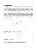
4.2 Design of tap feed structure [14]
4.2.1 Derivation of equation for input impedance
The tap feed method has been used for the impedance matching of a small loop antenna
[15]. The tap is designed using the equivalent electric circuit. The tap configuration for the
NMHA is shown in Fig. 4.2. The antenna parameters D and H are selected such that self-
resonance occurs at 315 MHz. The tap is attached across the center of the NMHA, and the
tap width and tap length are denoted as a and b, respectively. The equivalent electric circuit
is shown in Fig. 4.3. Here, L, C, and R are the inductance, capacitance, and input resistance,
respectively. The tap is excited by the application of a voltage V; M
A
is the mutual
inductance between the NMHA and the tap.
In the network circuit shown in Fig. 4.3, the circuit equations for the NMHA and the tap are
as follows:
1
() ()0
A
AAAT
Rj LM I jMI I
jC
ωω
ω
⎧⎫
⎪⎪
⎨⎬
⎪⎪
⎩⎭
+
+− + −=
(4.1)
() ()
AA
TTA
T
j
LMI
j
MI I V
ω
ω
−
+−=
(4.2)
From the above equations, the input impedance (Z
in
= V/I
T
) of the NMHA can be deduced:
Design of a Very Small Antenna for Metal-Proximity Applications
97
22
2
2
22
22
11
()()()()
()
11
() ()
A
T
T
A
in
RL M L LL
RM
CC
Zj
RL RL
CC
ωωω ωω
ω
ωω
ωω
ω
ω
−−+−
=+
+− +−
(4.3)
Here, the tap inductance (L
T
) is given by [16]:
22
22 22
44
ln( ) ln( ) 2( /2 )
()()
T
ab ab
Lb a d abba
db a b da a b
μ
π
⎡⎤
⎢⎥
=++++−−
⎢⎥
++ ++
⎣⎦
(4.4)
H
A
D
A
b
a
~
N
d
Fig. 4.2 Tap configuration for NMHA
C
A
R
A
L
A
L
T
~
V
I
A
I
T
NMHA
Tap
M
A
Fig. 4.3 Equivalent circuit for tap feed
4.2.2 Simple equation for step-up ratio
At the self-resonant frequency (
ω
r
= 2πf
r
), the imaginary part of Eq. (4.3) becomes zero.
Therefore, we have
22 2
11
()()()()0
rT r A r r
rr
RL M L L
CC
ωωω ω
ωω
−
−+−=
(4.5)
If the variable of the above equation is replaced by (ω
r
L – 1/ ω
r
C) = α, this expression
becomes second-order in α. The two solutions are
Advanced Radio Frequency Identification Design and Applications
98
22422
4
()
2
rA r A T
T
M
MRL
L
ωω
α
±−
±=
(4.6)
We label these two solutions α(+) and α(-). For these α values, the resonant points are
shown in Fig. 4.4.
Rin:α(+)
Rin:α(-)
Fig. 4.4 Resonant points
In the root of Eq. (4.6), the following assumption is applicable. This assumption is valid
when the tap width (a) is nearly equal to the antenna diameter (D):
24 22
4
rA T
M
RL
ω
〉〉 (4.7)
Then, the expression for α becomes simple:
2
()
rA
T
M
L
ω
α
+=
(4.8)
By using α(+) in Eq. (4.3), we can derive an expression for the input resistance (R
in
):
2
(/ )
in T A
RRLM= (4.9)
Finally, the step-up ratio (γ) of the input resistance can be simply expressed as
()
2
/
TA
LM
γ
= (4.10)
The important point to be noted in this equation is that M
A
has a strong effect on the step-up
ratio. In the following section, the calculation method and M
A
results are presented.
4.2.3 Calculation method and results for mutual inductance
The calculation structure is shown in Fig. 4.5. B
A
is the magnetic flux density in the NMHA,
and I
T
is the tap current.
M
A
can be calculated using the following equation [17]:
Design of a Very Small Antenna for Metal-Proximity Applications
99
a
~
b
B
i
B
i
B
0
B
j
B
j
B
A
I
T
D
A
H
A
NMHA
Tap feed
Fig. 4.5 Calculation structure
AA
SS
A
TT
dd
M
II
μ
⋅
⋅
==
∫∫
BS HS
(4.11)
Here,
B
A
is the sum of the B
i
values of each loop in Fig. 4.5. The magnetic field (H
i
) in each
loop is given by
0
2
sin
4
T
i
l
I
Hdl
r
θ
π
=
∫
(4.12)
Here, r represents the distance between a point on the tap and a point inside a loop. In this
calculation, a current I
T
exists at the center of the tap wire. Therefore, even if the the
magnetic field is applied at point close to the tap wire.
0.021
0.005
0.020
0.014
A
B
C
N=5
N=7
N=11
f=315 MHz
d=0.55 mm
D
E
Fig. 4.6 Study structures of NMHA
Advanced Radio Frequency Identification Design and Applications
100
To establish the design of the tap feed, the L
T
/M
A
values in Eq. (4.10) must be represented
by the structural parameters. Calculations are performed for the structures shown in
Fig. 4.6. Points A, B, and C are used to investigate the dependence of M
A
on the structural
parameters.
0.5 0.6 0.7 0.8 0.9 1.0
1.0
1.5
2.
0
a/D
A
b/D
A
Eq. (4.11)
0.4 0.5
0.6
(M
A
/L
0
)
A
0.50.60.70.80.91.0
1.0
1.5
2.
0
a/ D
A
b/D
A
0.15
(M
A
/L
0
)
B
Eq. (4.11)
A structure×0.34
0.19 0.23
0.5 0.6 0.7 0.8 0.9 1.0
1.0
1.5
2.
0
a/D
A
b/D
A
0.16
(M
A
/L
0
)
C
0.20 0.24
Eq. (4.11)
A structure×0.37
Fig. 4.7 Calculated results: M
A
/L
0
The calculated M
A
values are shown in Figs. 4.7(a), (b), and (c). The M
A
value is normalized by
the L
0
value, which is the self-inductance of a small loop with diameter D. L
0
is given by [18]
0
8
ln( ) 1.75
2
DD
L
d
μ
⎧
⎫
=−
⎨
⎬
⎩⎭
(4.13)
Structure A in Fig. 4.7(a) is used as a reference to determine the dependence of M
A
on the
structural parameters. Comparison of structures A and B reveals the dependence of M
A
/L
0
on H
A
and D
A
. Taking into account Eq. (4.11), we show that M
A
is proportional to D
A
/H
A
.
The D
A
/H
A
value for structure B becomes 0.34 times that for structure A. In Fig. 4.7(b), the
solid lines indicate the calculated results obtained using Eq. (4.11). The dotted lines indicate
the transformed values, i.e., the product of the values in Fig. 4.7(a) and 0.34. The data
corresponding to the solid and dotted lines are in good agreement, thus confirming that the
M
A
/L
0
values are proportional to the D
A
/H
A
value. We now compare structures A and C. Eq.
(4.11) shows that M
A
is proportional to N/H
A
. The N/H
A
value for structure C is 0.37 times
that for structure A. In Fig. 4.7(c), the solid lines indicate the calculated results obtained
using Eq. (4.11). The dotted lines indicate the transformed values, i.e., the product of the
values shown in Fig. 4.7(a) and 0.37. The solid and dotted lines agree well, confirming the
proportional relationship between M
A
/L
0
and N/H
A
value. We thus have
Design of a Very Small Antenna for Metal-Proximity Applications
101
0
AA
A
M
DN
LH
∝ (4.14)
4.2.4 Universal expression for M
A
The design equation becomes universal if the M
A
/L
0
value is expressed in terms of M
0
/L
0
.
Here, M
0
is the mutual inductance between the one-turn loop and a tap. If we introduce a
coefficient
α
A
, M
A
/L
0
can be given by
0
00
AA
A
A
M
MDN
LHL
α
= (4.15)
The M
0
/L
0
values calculated using from Eq. (4.11) (assuming N = 1) are shown in Fig. 4.8.
The M
0
/L
0
values show small deviations with the D
A
values. If all the structural deviations
depending on D
A
, H
A
, and N are contained in the coefficient term,
α
A
can be expressed as
follows:
2
0.05 0.0075 4.5( )
H
N
ND
α
=+ +
(4.16)
We use D
A
= 0.020λ (see Fig. 4.8) for the M
0
/L
0
values.
M
0
/L
0
0.12
D
A
=0.014λ
D
A
=0.020λ
D
A
=0.029λ
0.17
Fig. 4.8 Calculated results: M
0
/L
0
4.2.5 Design equation for step-up ratio in NMHA tap feed
By applying Eq. (4.15) to Eq. (4.10), we can express the step-up ratio (γ) as follows:
Advanced Radio Frequency Identification Design and Applications
102
2222
0
0
()( )()( )
TATA
A
AA AA
LHLH
MDNMDN
γ
γ
αα
== =
(4.17)
This equation is the objective design equation for a tap feed. Here, γ
0
is given by
2
0
0
()
T
L
M
γ
=
(4.18)
The calculated γ
0
values are shown in Fig. 4.9. For each γ
0
, the tap structural parameters a/D
A
and b/D
A
are given.
40
80
120
γ
0
=(L
T
/M
0
)
2
D
A
=0.014λ
D
A
=0.020λ
D
A
=0.029λ
Fig. 4.9 Calculated results: γ
0
4.2.6 Design procedure for tap feed
We now summarize the design procedure. First, the self-resonant NMHA structure is
determined on the basis of Fig. 3.2 or Eq. (3.16). Then, the antenna input resistance is
estimated using Eqs. (3.2), (3.4), and (3.19). The requested γ value is determined by taking
into account the feeder line impedance. Then, Eq. (4.17) is used to determine the tap
structure. The γ
0
value is determined by substituting the antenna parameters and γ value in
Eq. (4.17). The final step involves the use of the data provided in Fig. 4.9. The objective γ
0
curve in Fig. 4.9 is identified Then, the relation between a/D
A
and b/D
A
is elucidated, and a
suitable combination of a/D
A
and b/D
A
is selected.
5. Antenna design for RFID tag
In this section, the proximity effect of a metal plate on the self-resonant structures and
radiation characteristics of the antenna is clarified through simulation and measurement. An
Design of a Very Small Antenna for Metal-Proximity Applications
103
operating frequency of 953 MHz is selected, and antenna sizes of 0.03λ–0.05λ are considered.
We discuss the fabrication of tag antennas for Mighty Card Corporation [19].
5.1 Design of low-profile NMHA [20]
The projection length of the NMHA is reduced by adopting a rectangular cross section, so
that the antenna can be used in an RFID tag. The simulation configuration is shown in Fig.
5.1. The antenna thickness is T, and the size of the metal plate is M. The spacing between the
antenna and the metal plate is S. The equivalent electric and magnetic currents are I and J,
respectively. E
θ
and E
φ
correspond to the radiation from the electric and magnetic currents,
respectively.
x
y
T
φ
E
φ
E
θ
I
J
z
θ
M
M
W
L
Fig. 5.1 Simulation configuration
The most important aspect of the antenna design is the self-resonant structure. The self-
resonant structure without a metal plate is shown in Fig. 3.10. The design equation
(Eq. (3.16)) is not effective when a metal plate is present in the vicinity of the antenna.
Therefore, the self-resonant structure is determined by electromagnetic simulations. The
calculated self-resonant structures are shown in Fig. 5.2; T and N are variable parameters.
Other parameters, such as d, S, and M are shown in the figure. For small values of T, large W
values are required so that the cross-sectional area is maintained at a given value. For
smaller values of N, too, large W values are required so that the individual inductances of
the cross-sectional areas are increased.
An example of the input impedance in the structure indicated by the triangular mark at
T = 3 mm is shown in Fig. 5.3. At 953 MHz, the input impedance becomes a pure resistance
of 0.49 Ω. Because the antenna has a small length of 0.04
λ
, the input resistance is small. The
radiation characteristics are shown in Fig. 5.4. To simplify the estimation of the radiation
level, the input impedance mismatch is ignored by assuming a “no mismatch” condition in
the simulator. The dominant radiation component is E
φ
,, which corresponds to the magnetic
current source. Surprisingly, an antenna gain of –0.5 dBd is obtained under these conditions.
Here, the unit dBd represents the antenna gain normalized by that of the 0.5
λ
dipole
antenna. The high gain is a result of the appropriate choice of the ohmic resistance (R
l
) on
Advanced Radio Frequency Identification Design and Applications
104
the basis of the radiation resistance (R
r
). R
l
is determined from the antenna wire length and d
given by Eq. (3.19). Here, because R
r
is 0.24 Ω, R
l
should be smaller than this value. To
achieve a small ohmic resistance, d should be made as large as possible. When d is 0.8 mm,
R
l
is 0.25 Ω, and hence, a radiation efficiency of about 50% is achieved. This antenna gain
confirms that a small rectangular NMHA in close proximity to a metal can be used in
several practical applications.
0.03 0.04 0.05
0.02
0.03
0.04
0.05
0.06
0.07
0.08
0.09
0.1
T=1mm
T=3mm
N=4
N=5
N=6
N=4
N=5
N=6
X
L
= X
D
X
L
' = X
D
'
Antenna length (L/λ)
Antenna width (W/λ)
Frequency=953MHz, d=0.8mm
Metal p late size:M=1λ, S=1mm
Fig. 5.2 Self-resonant structures
M / λ
953MHz
0.49Ω
940
965
Fig. 5.3 Input impedance
Design of a Very Small Antenna for Metal-Proximity Applications
105
E
θ
= -20dBd
E
φ
= -0.5dBd
M
E
T
A
L
1mm
Fig. 5.4 Radiation characteristics
T=3mm
N=4
T=1mm
E
φ
E
θ
T=3mm
T=1mm
N=5
N=6
Magnetic
current source
Electric
current source
M=1 wavelength
Fig. 5.5 Radiated field components
Advanced Radio Frequency Identification Design and Applications
106
The important antenna gain characteristics for the self-resonant structures are shown in
Fig. 5.5. It is noteworthy that the E
φ
components are dominant, while the E
θ
components are
less than –20 dBd. There is no difference in the antenna gain even when N is changed. For
large T values, a high antenna gain is achieved. When T is 3 mm, the gain is expected to be
comparable to that of a 0.5
λ
dipole antenna. Moreover, the antenna gain remains constant
for different values of L. Hence, excellent antenna gains may be obtained for small antenna
sizes such as 0.03
λ
.
5.2 Practical antenna characteristics
A high gain can be expected for a small NMHA. However, because the input resistance of
such an antenna is small, an impedance-matching structure is required for practical
applications. A tap-matching structure is used for a 50-Ω coaxial cable, as shown in Figs.
5.6(a) and (b). The tap structure is rather simple. Wire diameters of 0.8 mm and 0.5 mm are
selected for the antenna and the tap, respectively. Because the spacing between the antenna
and the metal plate is small (1 mm), appropriate arrangement of the tap arms is important.
L : 12.6mm
(0.04λ)
W : 12.3mm
(0.039λ)
Tap
Metal plate
Antenna
(a) Perspective view
T:3mm
(0.01 )
Metal plate
F
1
:12.3mm
d:0.5mm
S:1mm
F
2
:4mm
(b) Cross-sectional view
Fig. 5.6 Experimental NMHA structure
The fabricated antenna and feed cable are shown in Fig. 5.7. The tap arms are soldered to the
antenna wire, and a coaxial cable is used as a feed line. A Sperrtopf balun is attached to the
coaxial cable to suppress leak currents. Figure 5.8 shows the measured and calculated
antenna impedances. The measured and calculated values are in good agreement, both in
Design of a Very Small Antenna for Metal-Proximity Applications
107
the presence and absence of the tap feed. When the tap feed is used, the antenna impedance
is exactly 50 Ω, and this confirms the effectiveness of the tap feed. The bandwidth
characteristics are shown in Fig. 5.9. A 3.5-MHz bandwidth is obtained when VSWR < 2.
This bandwidth corresponds to 0.4% of the center frequency.
L : 12.6mm
(0.04λ)
W : 12.3mm
(
0.039
λ
)
Tap
Antenna
Balun
Coaxial
cable
Fig. 5.7 Fabricated NMHA structure
953MHz
Cal.
Meas.
Without tap
feed
0.49Ω
50Ω
With
tap feed
Fig. 5.8 Input impedance
The important radiation characteristics observed when the antenna is placed near a metal
plate are shown in Fig. 5.10. The separation S in this case is 1 mm. A square metal plate with
a size of 0.5
λ
is used. The E
φ
component is dominant when the antenna is in close proximity
to the metal plate. A high antenna gain of –0.5 dBd is achieved. The E
φ
level in the presence
of the metal plate exceeds that in the absence of the metal plate by about 10 dB. The
usefulness of the NMHA in a metal-proximity application is verified. At the same time, the
intensity of the E
θ
component decreases to –11 dBd. This shows that the electrical current
source does not work well under metal-proximity conditions.
Advanced Radio Frequency Identification Design and Applications
108
Fig. 5.9 VSWR characteristics
E
θ
= −10.4
E
φ
= −0.53dBd
E
θ
= − 10.1
E
φ
= − 0.53dBd
Cal.(dotted) Meas.(solid)
Fig. 5.10 Radiation characteristics
5.3 RFID tag antenna
In order to use the rectangular NMHA as a tag antenna, the input impedance must be
matched to the IC impedance of Z
IC
= 25 – j95 Ω. Therefore, the antenna size and tap size are
modified as shown in Fig. 5.11. The tap length is increased to obtain the necessary
inductance for achieving conjugate matching with the IC capacitance. The spacing between
the antenna and the metal plate is set to 1.5 mm. A 0.5
λ
square metal plate is used. The
impedance-matching process is shown in Fig. 5.12. The tap length (T3) is important for
matching the impedance to the IC. Almost complete conjugate matching can be achieved at
T3 = 17 mm.