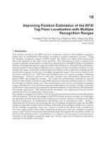
Advanced Radio Frequency Identification Design and Applications Part 7 pdf
Bạn đang xem bản rút gọn của tài liệu. Xem và tải ngay bản đầy đủ của tài liệu tại đây (2.42 MB, 20 trang )
Design of a Very Small Antenna for Metal-Proximity Applications
109
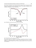
L : 15.7mm
W : 14.3mm
1mm
Wire diameter of the tag:0.5mm
27mm
N=6
(a) Perspective view
H:3.15mm
T2:1mm
T3:17mm
Metal plate
IC chip
T1:10mm
S:1.5mm
(b) Cross-sectional view
Fig. 5.11 Configuration of RFID tag antenna
W
ithout tap
T3= 17mm
T3= 9mm
Meas.
Cal.
IC chip
953MHz, 0.49Ω
953MHz, 25+j95Ω
Fig. 5.12 Input impedance
Advanced Radio Frequency Identification Design and Applications
110
M
E
T
A
L
1.5mm
E
θ
= -13.3dBd
E
φ
= -0.4dBd
Fig. 5.13 Radiation characteristics
IC chip
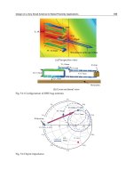
W:14.3mm(0.045λ)
L:15.7mm
(0.05λ)
T:3.15mm
(0.01λ)
22mm(0.07λ)
7mm(0.02λ)
0.5mm
NMHA
Tap f e ed
d:1mm
Foamed polystyrene (t=1.5mm)
Metal plate
Fig. 5.14 Fabricated antenna
Design of a Very Small Antenna for Metal-Proximity Applications
111
To estimate the antenna gain of this structure, we evaluate the radiation characteristics; the
results are shown in Fig. 5.13. The antenna input impedance is designed to be
Z
ANT
= 25 + j95 Ω. To simplify the radiation intensity calculation, the input-impedance
mismatch is ignored by adopting the “no mismatch” condition. An antenna gain of –0.4 dBd
is obtained in this case. Therefore, the electrical performance is expected to be comparable to
that of conventional tags.
On the basis of these results, we fabricate an actual antenna with a help of Mighty Card
Corporation, as shown in Fig. 5.14. This antenna is composed of a copper wire with a
diameter of 1 mm. The IC is inserted into the tap arm. The antenna and IC are placed on a
piece of polystyrene foam attached to the metal plate. The thickness of the foam is 1.5 mm,
and the size of the square metal plate is 0.5
λ
.
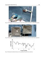
5.4 Read-range measurement
The read range is measured using the set-up shown in Fig. 5.15. A commercial reader
antenna is used for transmitting and receiving. This reader antenna is connected to a reader
unit and a computer. When the tag information is read, the tag number is shown on the
computer screen. Read-range measurements are conducted by changing the distance
between the reader antenna and the tag. The distance at which the tag number disappears is
considered to be the read range. These read ranges might be affected by the height pattern at
the measurement site, and hence, the height of the tag is so chosen that the highest possible
electrical strength is obtained.
Reader
Computer screen
15m
Tran/receive antenna
Rectangular NMHA
15cm
15cm
Fig. 5.15 Read-range measurement set-up
Advanced Radio Frequency Identification Design and Applications
112
The measured read ranges are summarized in Table 5.1. For conventional antennas placed
in a free space, read ranges of 9 m are obtained. In the case of a metal proximity use, read
ranges become very small. For the NMHA, read ranges of 6 m and 15 m are obtained
without and with the metal plate, respectively. The reason of this read range increase is
attributed to the antenna gain of Fig. 5.13. The effectiveness of the tag is confirmed by the
aforementioned read-range measurement.
Conventio
nal
Antenna
Antenna in free space
Read
range
Antenna in free space
Read
range
9m 9m
Low
profile
NMHA
Without a metal plate
Read
range
With a metal plate
Read
range
6m 15m
47mm
42mm
15mm
15mm
150mm
150mm
95mm
16mm
Table 5.1 Results of read-range measurement
6. Conclusions
A normal-mode helical antenna (NMHA) with a small size and high gain is proposed for
use as an RFID tag antenna under metal-plate proximity conditions. The important features
of the design are as follows:
1. Fundamental equations for important electrical characteristics have been summarized,
and useful databases have been shown.
2.
The antenna efficiency, which is related to the structural parameters, is important for
achieving high antenna gain.
3.
A simple design equation for determining the self-resonant structures has been
developed.
4.
For the fabrication of an actual antenna, the tap feed has been carefully designed so that
a small input resistance is obtained.
5.
A simple design equation for determining the tap-feed structures has been developed.
6.
A small RFID tag antenna that can be used under metal-plate proximity conditions has
been designed.
7.
A read range superior to that of conventional tags has been achieved.
Design of a Very Small Antenna for Metal-Proximity Applications
113
7. References
[1]
[2]
[3] Xuezhi Zeng, et al, “Slots in Metallic Label as RFID Tag Antenna,” APS 2007, pp.1749-
1752, Hawaii, June.2007.
[4] W.G. Hong, W.H. Jung and Y. Yamada, “High Performance Normal Mode Helical
Antenna for RFID Tags”, IEEE AP-S’07, pp.6023-6026, Hawaii, June 2007
[5] K. Tanoshita, K. Nakatani and Y. Yamada, “Electric Field Simulations around a Car of
the Tire Pressure Monitoring System”, IEICE Trans. Commu., Vol.E90-B, No.9,
2416-2422, 2007
[6] W. G. Hong, Y. Yamada and N. Michishita, Low profile small normal mode helical
antenna achieving long communication distance ”, Proceedings of iWAT2008,
pp.167-170, March 2008
[7] Q.D. Nguyen, N. Michishita, Y. Yamada and K. Nakatani, “Electrical Characteristics of a
Very Small Normal Mode Helical Antenna Mounted on a Wheel in the TPMS
Application”, IEEE AP-S’09, Session 426, No.4, June 2009
[8] J. D. Kraus, “ANTENNAS, second edition”, McGraw-Hill Book Company, pp. 333-338,
1988
[9] H.A. Wheeler, “Simple Inductance formulas for Radio Coils,” Proc.IRE, Vol.16, pp.1398-
1400, 1928.
[10] W. L. Stutzman and G. A. Thiele, “Antenna Theory and Design, second edition”, John
Wiley & Sons, Inc., pp. 43-47 and p.71, 1998
[11] W. L. Stutzman and G. A. Thiele, “Antenna Theory and Design, second edition”, John
Wiley & Sons, Inc., pp.71-75, 1998
[12] Q.D. Nguyen, N. Michishita, Y. Yamada and K. Nakatani, “Deterministic Equation for
Self-Resonant Structures of Very Small Normal-Mode Helical Antennas”, IEICE
Trans. Communications., to be published in May, 2011
[13] J. S. McLean, “A re-examination of the fundamental limits on the radiation Q of
electrically small antenna”, IEEE Trans. Antennas Propag., Vol.44, No.5, pp.672-
676, May 1996
[14] Q.D. Nguyen, N. Michishita, Y.Yamada and K. Nakatani, “Design method of a tap feed
for a very small no-mal mode helical antenna”, IEICE Trans. Communications., to
be published in Feb., 2011
[15] K. Fujimoto, A. Henderson, K. Hirasawa and J.R. James, ”SMALL ANTENNAS”,
Research Studies Press Ltd., pp.86-92,1987
[16] K. Fujimoto, A. Henderson, K. Hirasawa and J.R. James, ”SMALL ANTENNAS”,
Research Studies Press Ltd., pp.78,1987
[17] Simon Ramo, John R. Whinnery and Theodore Van Duzer, FIELDS AND WAVES IN
COMMUNICATION ELECTRONICS – Third Edition, JOHN WILEY&SONS, INC.,
pp.189-193, 1993
[18] W. L. Stutzman and G. A. Thiele, “Antenna Theory and Design, second edition”, John
Wiley & Sons, Inc., p.75, 1998
Advanced Radio Frequency Identification Design and Applications
114
[19]
[20] W.G. Hong, N. Michishita and Y. Yamada, “Low-profile Normal-Mode Helical
Antenna for Use in Proximity to Metal”, ACES Journal, Vol.25, No.3, pp.190-198,
March 2010
6
Using Metamaterial-Based Coplanar
Waveguide Structures for the
Design of Antennas on Passive UHF RFID Tags
Benjamin D. Braaten and Masud A. Aziz
North Dakota State University
United States
1. Introduction
Radio Frequency Identification (RFID) is becoming a very affordable and reliable way of to
track inventory items. Because of this, RFID systems have received considerable attention
from researchers, engineers and industry personnel. Particularly, researchers involved with
RFID systems have developed smaller antennas for tags deployed in these systems. Several
of these designs have involved meander-line antennas (Finkenzeller, 2003), metamaterial-
based designs (Dacuna & Pous, 2007) and various materials (Griffin et. al., 2006). This
chapter will describe the main parameters of interest in a RFID system using Friis’s
transmission equation. This will then be followed by a section on recent work on applying
RFID systems to smart shelves, metallic plates and livestock tracking. Then a section on
coplanar-waveguides (CPW) is presented followed by the design of metamaterial-based
CPW antennas for passive UHF RFID tags.
2. An introduction to passive RFID systems
RFID technology is an automatic means of object identification with minimal human
intervention or error (Qing & Chen, 2007). Recently, RFID technology has been extensively
used to improve automation, inventory control, tracking of grocery products in the retail
supply chain and management of large volumes of books in libraries (Jefflindsay, 2010;
Teco, 2010). RFID tags have functions similar to a bar code; however they can be detected
even when they are blocked by obstacles. RFID tags also carry more information than a bar
code (Finkenzeller, 2003).
A RFID system consists of a reader (or interrogator) and several tags (or transponders). A
typical RFID system is shown in Fig 1. The reader consists of a transmitting and receiving
antenna and it is typically connected to a PC or any other monitoring device. The tag has a
single antenna for both transmitting and receiving. Digital circuitry (or IC) that
communicates with the reader is attached to the antenna on the tag. The reader sends out an
electromagnetic field that contains power and timing information into the space around
itself (sometimes called the interrogation zone (Finkenzeller, 2003)). If there is a tag in the
interrogation zone, then the tag receives the electromagnetic field using its receiving
antenna. The tag then utilizes its IC to communicate with the reader. The IC collects power
Advanced Radio Frequency Identification Design and Applications
116
and timing information from the electromagnetic field and sends proper backscattered
messages to the reader using the transmitting antenna of the tag. The maximum distance
that a reader can interrogate a tag is termed as the max read range of the tag.
RFID
reader
To
PC
RFID
antenna
Incident electromagnetic field
from the reader
Backscattered electromagnetic
field from the ta
g
RFID ta
g
Fig. 1. Overview of a RFID system.
Depending upon the power source of the tag, a RFID system can be classified into three
major categories: active, semi-passive, and passive (Finkenzeller, 2003). An active tag uses
its own power from the battery attached to it to communicate with the reader. A semi-
passive tag also has its own battery but it is only awakened by the incident electromagnetic
field from the reader. This greatly enhances the read range of the tag (Finkenzeller, 2003). A
passive tag uses the power from the incident electromagnetic field. The incoming
electromagnetic field from the reader induces a port voltage on the tag antenna and the IC
uses its power harvesting circuit to provide power to the digital portion of the circuit. The
power is then used by the IC to communicate with the reader.
The RFID system can be described by the Friis transmission equation (Stutzman & Thiele,
1998):
()
rt
rt
GG
PP
q
R
2
2
4
λ
π
=
(1)
where
P
t
is the power transmitted by the reader, P
r
is the power received by the passive tag,
G
t
is the gain of the antenna on the reader, G
r
is the gain of the antenna on the tag, λ is the
free-space wavelength of the transmitting frequency by the reader,
R is the distance between
the antenna on the reader and the antenna on the tag and
q is the impedance mismatch
factor (0 ≤
q ≤ 1) between the passive IC and the antenna.
Equation (1) assumes a polarization match between the antenna used by the reader and the
antenna on the passive tag. Therefore, a good match between the passive IC and the antenna
on the tag is essential. It is also assumed that the tag is in the far-field of the reader.
Therefore, a larger gain of the antenna on the tag will mean more power for the passive IC
on the tag. Moreover, using a longer wavelength will also improve the power at the tag.
However, the power available to the tag reduces by the distance squared as the tag and
reader antenna are moved apart. Equation (1) can also be expressed as follows (Braaten et
al., 2008; Rao et al., 2005):
trt
r
qG G P
R
P
4
λ
π
=
. (2)
If the threshold power required to activate the IC on the tag is
P
th
, then maximum read
range
r
max
can be derived from Equation (2)
Using Metamaterial-Based Coplanar Waveguide Structures for the
Design of Antennas on Passive UHF RFID Tags
117
trt
max
th
qG G P
r
P
4
λ
π
= . (3)
Equation (3) is very useful for predicting the max read range of a passive RFID tag.
Generally,
P
th
of a RFID tag is known. Moreover, P
t
and G
t
are fixed. This leaves the two
variables
q and G
r
to the designer. Typically, a tag is designed to have the highest r
max
. One
way of achieving this is to have a good match between the antenna and the IC on the tag
with a large
G
r
.
3. Summary of previous work
3.1 RFID shelves
Recently, the RFID smart-shelf system has received considerable attention. This is due to the
increasing demands for large-scale management of such items as grocery products in the
retail supply chain, large volume of books in libraries, bottles in the pharmaceutical
industry, and important documentation in offices (Landt, 2005; Want, 2006). The RFID smart
shelf is a regular shelf with a reader antenna embedded in the shelf. This ideally allows for
only detecting the tagged items located on that shelf. Extending this concept to every shelf
in a store makes it possible to automatically locate and inventory every item.
There have been many different smart-shelves proposed by different authors. Design of a
smart-shelf can be found in both the High Frequency (HF) and Ultra-High Frequency (UHF)
range. The main difference is that at HF the energy coupling between the reader antenna
and the tag is essentially made through the magnetic field (Medeiros et al., 2008). A very
common reader antenna configuration is a loop antenna (Qing & Chen, 2007; Cai et. al.,
2007). Good coupling requires close proximity between the reader antenna and the tag. At
UHF, readers are equipped with antennas such as patch antennas (Lee et. al., 2005) and
energy coupling to the tag antenna is made through propagating waves.
At UHF, it is difficult to limit the antenna radiation exactly to the shelf boundary without
resorting to costly metal or absorbing shields. One solution can be to incorporate a leaking
microstrip line with an extended ground plane in the shelf. This shelf design exploits the
leaking fields from a microstrip line (undesirable in microwave circuits) for applications of
RFID systems in small areas (Medeiros et al., 2008).
3.2 Tags on metallic objects
There is a strong interest from many industries (aeronautics, automotive, construction, etc.)
in tagging metal items (airplane or automotive parts, metal containers, etc.) using both
active and passive RFID tags (Rao et. al., 2008). Unfortunately, tag performance is affected
by the electrical properties of metal objects that are in contact or close proximity to the tag
antenna. A series of measurements were used to measure the far-field gain pattern and gain
penalty of several tag antennas when connected to different objects (Griffin et. al., 2006). The
Antenna Gain Penalty (AGP) is defined to be the loss in gain of the antenna due to metal
attachment. The measured gain showed sufficient distortion due to permittivity, loss
tangent of the material, surface waves and diffraction (Griffin et. al., 2006).
The presence of the metal plate shifts up the resonant frequency of the HF reader loop
antenna and weakens the intensity of the magnetic field (Qing & Chen, 2007). When a metal
plate is positioned close to a loop antenna, the magnetic field generated by the loop antenna
reaches the surface of the metal plate. In order to satisfy the boundary conditions on the
Advanced Radio Frequency Identification Design and Applications
118
metal surface, the magnetic field normal to the surface must be zero. For this to occur, an
additional current, known as the eddy current, is induced within the metal plate. The
induced current opposes the magnetic flux generated by the antenna, which may
significantly dampen the magnetic flux in the vicinity of the metal surface. The damping of
magnetic flux leads to a reduction of the inductance of the loop antenna. Therefore, the
resonant frequency of the antenna is increased (Finkenzeller, 2003). The resonant frequency
of the antenna also depends on the position of the metal objects. The back-placed metal
(metal positioned at the back of the antenna) has the most significant impact on the resonant
frequency of the antenna as opposed to the side or bottom placed metal (Qing & Chen,
2007).
Several antennas have been proposed to overcome the abovementioned constraints. An
RFID tag with a thin foam backing material that is capable of operating efficiently both as a
dipole antenna and as a microstrip antenna has been proposed (Mohammed et. al., 2009).
The antenna behaves as a dipole antenna in free space and acts as a patch antenna when it is
attached to metal objects. A wideband metal mount RFID tag that works on a variety of
metals also was proposed (Rao et. al., 2008). Reduction in the size of the antenna also has
been achieved by introducing a quasi-Yagi antenna on a RFID tag (Zhu et. al., 2008). The
impact of a wooden and metallic surface together on the antenna has also been studied
(Kanan & Azizi, 2009).
3.3 Cattle tag research
RFID technology has many applications. One use of this technology is for livestock
identification. Animals such as cattle and sheep are tagged for purposes, such as disease
control, breeding management, and stock management (Ng et. al., 2005). Loop antennas
have been proposed as the RFID tag antenna in the cattle tags (Braaten et. al., 2006). One of
the reasons that loop antennas are widely used is that they are not required to be very large.
Loops are used as receiving antennas because the output of the loop is proportional to the
number of turns and the permeability of the material the loop is wound on. Therefore, weak
signals can be detected by using a loop with a large number of turns and wound on a
material with significant permeability. Antennas with dielectric superstrates have also been
proposed (Braaten et. al., 2008). It has been shown that a passive tag with a meander-line
antenna and dielectric superstrate can significantly augment the read range of the tag.
4. Coplanar-waveguide structures
Coplanar-waveguide (CPW) transmission lines are used extensively in wireless
communications (Pozar, 2005; Collin, 2001). A CPW transmission line is shown in Fig. 2.
The reference planes and signal plane are printed on the same conducting layer. Each plane
is usually made of a conducting material such as copper. The dielectric is typically isotropic
and ungrounded. The signal propagating down the CPW transmission line is symmetrically
guided between the signal plane and the outer reference planes. The advantages of a CPW
transmission line are that it only requires a single conducting layer and components can be
easily connected between the signal plane and the reference plane. This is very useful for
printed circuit boards with many different layers because only a single layer dedicated to
microwave signals is needed. The disadvantage of a CPW transmission line is the need to
keep both reference planes at the same potential all along the signal trace. This can be
difficult to do on a single conducting layer.
Using Metamaterial-Based Coplanar Waveguide Structures for the
Design of Antennas on Passive UHF RFID Tags
119
Many advances have been made on the CPW transmission line. For example novel filters
have been developed (Velez et al., 2009) and right/left-handed propagation has been
demonstrated (Eleftheriates and Balmain, 2005) on CPW transmission lines. Many of the
new techniques and structures that have been developed can also be used for the design of
new antennas. The following section uses a new structure developed for CPW filters to
reduce the overall size of printed dipoles.
Fig. 2. A CPW transmission line on a dielectric substrate.
5. Metamaterial-based antenna design using OCSRR and MOCSRR particles.
Antennas on a passive UHF RFID tag are typically printed on the top side of a thin flexible
substrate while adhesive is applied to the bottom side to attach the tag to a desired object.
Because of this, all the conducting material (i.e., copper) used for the antenna is constrained
to a single layer. This restriction requires the entire topology of the antenna to be printed on
the same plane. Many different types of meander-line antennas for passive UHF RFID tags
printed on a single conducting layer have been proposed (Marrocco, 2003; Calabrese et al.,
2008). Many of these meander-line antennas have proven to be useful, however recently a
special type of printed dipole (Braaten, 2010a; Braaten et al., 2010b) based on the meander-
line structure has recently been developed. Particularly, these newly developed printed
antennas use open complementary split ring resonator (OCSRR) and meander open
complementary split ring resonator (MOCSRR) particles connected in series to form
electrically small resonant dipoles (Velez et al., 2009).
5.1 The OCSRR particle
First, the OCSRR particle is introduced. The layout of each individual OCSRR particle is
show in Fig. 3 (a). Each particle is a coplanar-waveguide (CPW) structure with various
concentric ring gaps etched from the copper. A port is defined on each side of the particle
and the equivalent circuit in Fig. 3 (b) is used to model the OCSRR particle in Fig. 3 (a). The
equivalent inductance
L
eq,o
represents the inductance between ports a and b caused by the
ring between the ring slots connecting the two ports and the equivalent capacitance
C
eq,o
represents the distributed capacitance between ports a and b caused by the ring slots. Each
section of the meander-line antenna in Fig. 4 has the same equivalent circuit as the OCSRR
particle in Fig. 3 (b). Therefore, by connecting several OCSRR particles in series, an alternate
electrically small resonant antenna can be designed.
Advanced Radio Frequency Identification Design and Applications
120
5.2 Equivalent circuit and the dimensional relation of the OCSRR particle
To illustrate the behaviour of the OCSRR particle in Fig. 3, the equivalent circuit is extracted
and discussed in this section for various values of
r
d
(i.e., inner disc radius values) of the
OCSRR particle. The CPW structure shown in Fig. 5 can be used to extract the equivalent
circuit of the OCSRR particle (Velez et al., 2009). A convenient method of extracting the
equivalent circuit is to use a commercially available full wave electromagnetic solver such as
Momentum (Advanced Design System 2009a) to simulate the CPW structure in Fig. 5. When
the particles resonate, the impedance on the 50 Ω CPW transmission line caused by the
particles is infinity. This will result in an optimum match (i.e., lowest
S
11
values) between
the 50 Ω ports and 50 Ω CPW transmission line to occur at resonance. Then, from the
simulated S
11
values, an equivalent circuit can be extracted using a curve fitting technique.
This equivalent circuit can then be placed in the location of the OCSRR particle in Fig. 3 and
be used to represent the physical OCSRR particle. The equivalent circuit loads the 50 Ω CPW
transmission line in a manner similar to the actual OCSRR particles. With a technique to
extract the equivalent circuit of the OCSRR particle, a designer is able to determine how
various dimensions of the OCSRR particle ultimately affect the equivalent circuit of that
particular particle. Particularly, how the dimensions affect the individual capacitance and
inductance values of the equivalent circuit of the OCSRR particle can be shown.
Using the method described in the previous paragraph, the equivalent circuit of the OCSRR
particle in Fig. 3 (a) was extracted for various dimensions of the inner disc (i.e., for various
values of
r
d
) and scale factors (i.e., for various values of S). For the various values of r
d
the
dimensions of the OCSRR particle were w = 8.3 mm, h = 8.1 mm, s = 0.51 mm, m = 0.47 mm,
n = 0.39 mm, r
i
= 0.45 mm and t = 0.39 mm. The substrate was defined to be 1.36 mm thick
and had a permittivity of 4.2. The values of M and N in Fig. 5 are 0.4 mm and 3.1 mm,
respectively. The results from these computations are shown in Table 1. The results in Table
1 can be used to design an OCSRR particle with a specific resonant frequency.
Fig. 3. (a) Layout of the OCSRR particle (the gray area is the copper) and (b) the equivalent
circuit of the OCSRR particle.
Fig. 4. Layout of a meander-line dipole.
h
Using Metamaterial-Based Coplanar Waveguide Structures for the
Design of Antennas on Passive UHF RFID Tags
121
Fig. 5. CPW structure used to extract the equivalent circuit of the OCSRR particle (the gray
area is the copper).
r
d
(mm) L
eq
(nH) C
eq
(pF) f
0
(GHz)
1.0 1.5 2.95 2.39
1.2 1.5 2.95 2.39
1.4 1.5 3.0 2.37
1.6 1.5 3.0 2.37
1.8 1.4 3.25 2.35
2.0 1.7 3.05 2.2
2.2 1.7 3.05 2.2
Table 1. Equivalent circuit design table for the OCSRR particle for various values of r
d
.
S
L
eq
(nH) C
eq
(pF) f
0
(GHz)
0.7 1.0 2.85 2.98
0.75 1.1 2.9 2.81
0.8 1.3 2.85 2.61
0.85 1.2 3.2 2.56
0.9 1.4 3.15 2.39
0.95 1.4 3.25 2.35
1.0 1.7 3.05 2.2
Table 2. Equivalent circuit design table for the OCSRR particle for various scale factors S.
Next, the dimensions of OCSRR particle were fixed at w = 8.3 mm, h = 8.1 mm, s = 0.51 mm,
m = 0.47 mm, n = 0.39 mm,
r
i
= 0.45 mm, r
d
= 2.0 mm and t = 0.39 mm. Starting from these
dimensions the particles were scaled by several factors symmetrically in both the x- and y-
directions. For example, for a scaling factor of S = 1.0, the dimensions of the particle are
unchanged. Then by scaling the particle by 0.8, every dimension of the particle is reduced by
Advanced Radio Frequency Identification Design and Applications
122
20%. A scaling factor of 0.7 then reduces the size of the particle by 30% and so on. The
equivalent circuit and resonant frequency was computed for each scaling factor using the
CPW structure in Fig. 5. The results from these computations are shown in Table 2.
5.3 Discussion
The results in Table 1 show how the resonant frequency of the OCSRR particle can be
reduced by increasing the radius value of the inner disc. This is expected, because the
equivalent capacitance of the particle is larger for larger radius values. The increased
capacitance is a result of the smaller ring gap. As the distance between the conducting inner
disk and the conducting ring (in the ring gap) reduces, the capacitance between the two
conductors increase which results in a lower resonant frequency.
The results in Table 2 show how the resonant frequency is related to different scaling factors
of the OCSRR particle. The resonant frequency of the particle was increased by
approximately 6 – 7% for a 5% change in the scaling factor. This is very useful for designing
an OCSRR particle for a specific resonant frequency.
5.4 Antenna designs using the OCSRR particle
OCSRR particles can be connected in series in a manner shown in Fig. 6 to form an
electrically small resonant dipole. In fact, a dipole consisting of series connected OCSRR
particles have characteristics similar to the meander-line dipole in Fig. 4. The equivalent
circuit of each meander-line section is a capacitor connected in parallel with an inductor.
The vertical traces in each meander-line section contribute to the equivalent capacitance and
the current travelling on each horizontal segment contributes to the equivalent inductance.
The equivalent circuit of an OCSRR particle is the same as the equivalent circuit of each
meander-line section. Therefore, by connected OCSRR particles in series, an alternate to the
meander-line dipole can be designed. Furthermore, it turns out that the overall size of a
dipole with series connected OCSRR particles is much smaller than a meander-line dipole
with the same resonant frequency.
Fig. 6. Layout of the printed dipole using series connected OCSRR particles (the gray area is
the copper).
The characteristics of the OCSRR dipole in Fig. 6 have been previously studied (Braaten,
2010a) and the results are summarized here in Tables 3 and 4. Table 3 shows how the input
impedance of the OCSRR antenna in Fig. 6 changes for various values of ε at a frequency of
920 MHz. The results in Table 4 show how the input impedance changes for various values
of
d (i.e., substrate thickness) at a frequency of 920 MHz. Using the results in Tables 3 and 4,
a designer will be able to predict how the input impedance of the antenna on the tag may
change by being attached to a particular item. Knowing this information is useful for
Using Metamaterial-Based Coplanar Waveguide Structures for the
Design of Antennas on Passive UHF RFID Tags
123
designing a successful antenna on a passive UHF RFID tag. Notice that the gain is mostly
unaffected except for thicker substrates.
A prototype passive UHF RFID tag using the OCSRR antenna in Fig. 6 has also been
presented and tested (Braaten, 2010a). The read range of the prototype tag was > 5 m with
overall dimensions of W = 55.54 mm and H = 11.91 mm. These overall dimensions are much
smaller than many commercially available tags.
ε
f
0
(MHz)
Z
in
(Ω)
G (dB)
1.0 920 6.6-j94.7 1.82
2.2 920 7.9-j27 1.89
4.25 920 13.8+j110 1.89
5.8 920 36.5+j375 1.76
Table 3. Input impedance and gain of the OCSRR antenna at 920 MHz for various values of ε.
d (mm)
f
0
(MHz)
Z
in
(Ω)
G (dB)
0.127 920 7.4-j49 1.87
0.787 920 13.8+j110 1.88
1.57 920 28.1+j288 1.70
3.14 920 93+j677 1.35
Table 4. Input impedance and gain of the OCSRR antenna at 920 MHz for various values of d.
5.5 The MOCSRR particle
Next, the characteristics of the MOCSRR particle are investigated. The layout of an
individual MOCSRR particle is shown in Fig. 7 (a). This particle is similar to the OCSRR
particle except the ring slots take a meander route between ports a and b and not a circular
route as in the OCSRR particle. This meander route results in a much lower resonant
frequency for over all dimensions similar to an OCSRR particle. This lower resonant
frequency is very useful for designing small resonant dipoles which is important for
designing small efficient passive RFID tags.
5.6 Equivalent circuit and the dimensional relation of the MOCSRR particle
Using the CPW structure in Fig. 8 and the method discussed in section 5.2, the equivalent
circuit is extracted for the MOCSRR particle for various values of δ and scaling factors. The
dimensions of the MOCSRR particle in Fig. 7 are y = 8.2 mm, x = 8.05 mm, c = 0.42 mm, v =
0.22 mm, d = 2.92 mm, h = 5.17 mm, t = 0.33 mm, g = 0.31 mm and q = 0.43 mm. The
substrate was defined to have a thickness of 1.36 mm and a permittivity of 4.2. The values
of M and N in Fig. 8 were 0.4 mm and 3.1 mm, respectively. The overall dimensions of the
MOCSRR particle and the OCSRR particle are similar to show the differences between the
equivalent circuits of each particle.
The results of these computations are shown in Tables 5 and 6. Table 5 shows how the
resonant frequency can be reduced by increasing the value of δ while the results in Table 6
show how the resonant frequency of the MOCSRR particle is related to the scaling factor
Advanced Radio Frequency Identification Design and Applications
124
and δ = 1.54 mm. For a 5% reduction in the overall size of the particle, a 100 MHz increase
in resonant frequency has been observed (i.e., the resonant frequency is approximately
reduced 5 – 6% for each scale step).
Fig. 7. (a) Layout of the MOCSRR particle (the gray area is the copper) and (b) the equivalent
circuit of the MOCSRR particle.
Fig. 8. CPW structure used to extract the equivalent circuit of the OCSRR particle (the gray
area is the copper).
δ (mm)
r
s
(mm) L
eq
(nH) C
eq
(pF) f
0
(GHz)
0.9 1.6 3.6 2.9 1.55
1.0 1.7 3.8 2.75 1.55
1.1 1.8 3.7 2.85 1.55
1.2 1.9 3.4 3.1 1.55
1.3 2.0 3.4 3.15 1.53
1.4 2.1 3.5 3.1 1.52
1.5 2.2 3.7 3.25 1.45
Table 5. Equivalent circuit design table for the MOCSRR particle for various values of
dimension
r
s
and δ.
Using Metamaterial-Based Coplanar Waveguide Structures for the
Design of Antennas on Passive UHF RFID Tags
125
S L
eq
(nH) C
eq
(pF) f
0
(GHz)
0.7 2.4 2.25 2.16
0.75 2.7 2.45 1.95
0.8 2.9 2.6 1.83
0.85 2.9 2.9 1.73
0.9 3.2 2.95 1.63
0.95 3.4 3.1 1.55
1.0 3.7 3.25 1.45
Table 6. Equivalent circuit design table for the MOCSRR particle for various scale factors S.
5.7 Discussion
Comparing the results in Table 1 to the results in Table 5 shows how much the resonant
frequency of the particle is reduced by using a meander ring slot instead of a circular ring
slot. This is because the results in Tables 1, 2, 5 and 6 show that the MOCSRR particle has
approximately twice the inductance as the OCSRR particle while the capacitance is
comparable. This is very useful for antenna miniaturization because the impedance of the
particles is inductive. This inductive property can be used for matching transmission lines
to the capacitive input impedance of electrically small antennas.
5.8 Antenna designs using the MOCSRR particle
MOCSRR particles can be connected in a similar manner to the series connected OCSRR
particles shown in Fig. 6 in section 5.4. This will result in the layout show in Fig. 9. Since
the equivalent circuit of each MOCSRR particle has the same equivalent circuit of each
meander-line section in Fig. 4, an electrically small resonant dipole can be designed.
To understand the behaviour of the antenna in Fig. 9, the input impedance was computed
for various substrate values of permittivity and thicknesses. The results for a = 0.4 mm and
z = 1.09 mm are shown in Figs. 10 – 13 (particle dimensions are defined in section 5.6 with
δ = 1.54 mm).
Fig. 9. Layout of the printed dipole using series connected MOCSRR particles (the gray area
is the copper).
The results Figs. 10 and 11 show how the input impedance of the antenna is related to the
permittivity of the substrate. For these computations the substrate thickness was fixed at
d = 1.36 mm. For example, at 920 MHz the antenna is most appropriately matched to the
input impedance of the passive IC for a substrate permittivity of 4.2. This makes the antenna
Advanced Radio Frequency Identification Design and Applications
126
in Fig. 9 desirable for printing on FR4 substrates. Figs. 10 and 11 also show how the input
impedance can change dramatically for slightly lower and higher values of substrate
permittivity. This information is useful for a designer when a tag is placed on various items.
By understanding how the impedance of the antenna changes for various substrates, the
maximum read range of a tag used on multiple items could be predicted.
Fig. 10. Real part of the input impedance of the MOCSRR antenna for various values of ε.
Fig. 11. Imaginary part of the input impedance of the MOCSRR antenna for various values of ε.
Using Metamaterial-Based Coplanar Waveguide Structures for the
Design of Antennas on Passive UHF RFID Tags
127
The results in Figs. 12 and 13 provide further information on the behaviour of the MOCSRR
antenna. These results show how the input impedance changes with substrates of different
thicknesses. At 920 MHz the antenna in Fig. 9 has the optimum match at d = 1.36 mm.
Fig. 12. Real part of the input impedance of the MOCSRR antenna for various values of d.
Fig. 13. Imaginary part of the input impedance of the MOCSRR antenna for various values
of d.
Advanced Radio Frequency Identification Design and Applications
128
6. Future work
Many different future topics of research could be explored as a result of this work. Several of
these topics could involve work on a different type of CPW particle, left-handed
propagation using the MOCSRR particles or analytical relations between the resonant
frequencies of the particle to various geometrical values. Studying these topics could further
reduce the size of the resonant antennas presented here or significantly shorten the design
time for an engineer using these particular antennas on a passive RFID tag.
7. Conclusion
Initially in this work a RFID system has been introduced using the Friis transmission
equation. This introduction was then followed by recent applications of RFID systems and
an introduction of the CPW structure. This then lead to sections outlining the design of
small resonant dipoles with OCSRR and MOCSRR particles. Particularly, the results in
these sections showed how the resonant frequencies of the particles were extracted and
related to various geometrical dimensions and how the input impedance of the small
resonant dipoles was related to various substrates.
8. References
Advanced Design System 2009a, Agilent Technologies, www.agilent.com.
Braaten, B.D.; Feng, Y.; & Nelson, R.M., “High-frequency RFID tags: an analytical and
numerical approach for determining the induced currents and scattered fields,”
IEEE International Symposium on Electromagnetic Compatibility, pp. 58-62, August
2006, Portland, OR.
Braaten, B. D.; Owen, G. J.; Vaselaar, D.; Nelson, R. M.; Bauer-Reich, C.; Glower, J.; Morlock,
B; Reich, M.; & Reinholz, A., “A printed Rampart-line antenna with a dielectric
superstrate for UHF RFID applications,” in
Proceedings of the IEEE Interntational
Conference on RFID,
pp. 74-80, April, 2008, Las Vegas, NV.
Braaten, B. D., “A novel compact UHF RFID tag antenna designed with series connected
open complementary split ring resonator (OCSRR) particles,”
IEEE Transactions on
Antennas and Propagation
, vol. 58, no. 11, November, 2010a, pp. 3728 – 3733 2010a.
Braaten, B. D.; Aziz, M. A.; Schroeder, M. J.; and Li, H., "Meander open complementary split
ring resonator (MOCSRR) particles implemented using coplanar waveguides,"
IEEE International Conference on Wireless Information Technology and Systems,
Honolulu, Hawai, Aug. 28 - Sep. 3, 2010b.
Cai, A.; Qing, X.; & Chen, Z.N., “High frequency RFID smart table antenna,”
Microwave
Optical Technological Letters
, vol. 49, no. 9, September 2007, pp. 2074-2076.
Calabrese, C. & Marrocco, G., “Meander-slot antennas for sensor-RFID tags,”
IEEE Antennas
and Wireless Propagation Letters.,
vol. 7, pp. 5-8, 2008.
Collin, R. E. (2001).
Foundations for Microwave Engineering, 2
nd
ed., John Wiley and Sons, Inc.
Hoboken, New Jersey.
Dacuna, J. & Pous, R. “Miniaturized UHF tags based on metamaterials geometries,”
Building
Radio Frequency Identification for the Global Environment
, July 2007, [Online],
www.bridge-project.eu.