Advanced Radio Frequency Identification Design and Applications Part 9 pot
Bạn đang xem bản rút gọn của tài liệu. Xem và tải ngay bản đầy đủ của tài liệu tại đây (1.68 MB, 20 trang )
Fully Printable Chipless RFID Tag
149
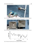
Fig. 31. Photograph of the experimental setup in the anechoic chamber of UWB RFID system.
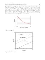
Fig. 32. Photograph of cross-polarized horn antennas used at reader end with 10cm separation.
-90
-85
-80
-75
-70
-65
-60
7891011
Frequency(GHz)
Isolation (dB)
Fig. 33. Measured isolation between cross-polarized reader horn antennas.
Chipless
Tag
Tx
Reader
A
ntenna
Rx
Reader
A
ntenna
Tx Antenna
Polarization
Rx Antenna
Polarization
Rx Antenna
Tx Antenna
107mm
100mm
Advanced Radio Frequency Identification Design and Applications
150
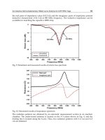
We encoded the tag with ID ‘0x000000’and placed it from 5 cm to 70 cm (in steps of 5 cm)
away from the horn reader antennas as shown in Fig. 31. The PNA was calibrated with the
output power at the ports being -28 dBm. Both amplitude and phase data were retrieved
when interrogating the tag. The chipless RFID tag was detected using a reference tag
“0x111111” which carried no resonances. Hence, when the two results were compared the
encoded resonances from tag ID ‘0x000000’ were successfully detected. The normalized
magnitude and phase of tag ID”0x000000” at 10 cm are presented in Figs 34 and 35
respectively. The measured results vs distance of tag from reader antennas are shown in Fig.
36.
-30
-25
-20
-15
-10
-5
0
7891011
Frequency (GHz)
Normalized Magintude (dB
)
Fig. 34. Normalized magnitude variation vs frequency of chipless RFID tag with
ID”0000000000000” from 7 – 10.7 GHz.
-150
-100
-50
0
50
100
150
7891011
Frequency (GHz)
Normalized Phase (Degrees)
Fig. 35. Normalized phase variation vs frequency of chipless RFID tag with
ID”0000000000000” from 7 – 10.7 GHz.
From Fig. 36 it is clear that in the anechoic chamber the tag can be detected further away (up
to 70 cm) when using phase data detection than when using amplitude data detection. This
is attributed to the greater robustness of phase when compared to amplitude. The successful
interrogation of the tag in both amplitude and phase was conducted up to 50 cm. This result
shows an improvement in the reading range detection of 300% in amplitude data and 75%
in phase data (up to 70 cm) compared with the results reported in the previous section. The
increased reading range in amplitude was greatly influenced by the increase of the cross-
polar isolation of the tag antennas, increased isolation between the reader horn antennas
and higher gain of the reader antennas (~11dBi over the entire band).
LSB
MSB
MSB
LSB
Fully Printable Chipless RFID Tag
151
0
20
40
60
80
100
5 152535455565
Distance (cm)
Accurately Read Tag (%)
Amplitude Data (anechoic chamber) Phase Data (anechoic chamber)
Amplitude Data (Laboratory) Phase Data (Laboratory)
Fig. 36. Number of successfully detected bits vs distance of tag from reader antennas from
7 – 10.7 GHz (maximum of 13 detectible bits).
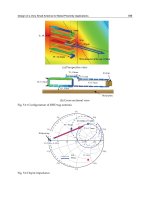
The chipless tag was placed in a laboratory setup (outside the anechoic chamber Fig. 37) in
order to measure the detection range of this particular setup when exposed to
environmental influences.
Fig. 37. Photograph of the experimental setup in the laboratory.
Fig. 36 shows that the tag was read accurately in both amplitude and phase up to 15 cm
when placed in a laboratory as shown in Fig. 37. The phase data were detectable at greater
reading ranges (up to 35 cm) than the amplitude data due to robustness of the phase data.
Fig 36 clearly shows that the reading range dropped by 50% outside the anechoic chamber
due to interference from the environment. However, it should be mentioned that the
detection procedure was a simple comparison of tag data with no resonances and tag data
with all resonances. The reading range could be improved by using signal processing
techniques (such as matched filtering) to isolate the tag signal from the noise and
interference and thus increase the reading range (Hartmann et al, 2004).
Maximum
number of
bits =13
Rx Antenna
Tx Antenna
Chipless
Tag
Tag Stand
Vector
Network
A
nal
y
zer
Advanced Radio Frequency Identification Design and Applications
152
5. Conclusion
In this chapter we have presented the development and testing of a chipless RFID tag based
on multiresonators. The development and successful testing of the chipless RFID tag meets
the demand for a fully-printable ultra-low cost tag used for tagging items on conveyor belts.
The salient feature of the novel chipless RFID tag is its fully-printable single-layered design
in a compact and low cost format. It has significant amount of data encoding capability (up
to 23 bits were designed).
Prior to the design and development of the chipless RFID tag a comprehensive literature
review of RFID tags was conducted. The goal of the literature review was to identify the
niche areas of design and development in RFID in which novel research could be carried
out. The comprehensive literature review of chipless RFID tags revealed that chipless tags
which are fully printable, multi-bit with ease of data encoding were not currently available.
Some work had been carried out on capacitively tuned dipoles and fractal Hilbert curve-
based tags but without the ability of data encoding.
The chipless RFID tag presented in this chapter comprises two main components: UWB
antenna and multiresonator. The multiresonating circuit consisted of cascaded spiral
resonators which operate at different resonant frequencies. Each resonant frequency
corresponded to a single data bit. The spiral resonator was chosen as the main encoding
element since it exhibits compact size, high Q and small bandwidth in comparison to other
planar resonators which exhibited stop-band performance.
Spectral signature encoding is used to encode data by the tag. Spectral signature requires a
one to one (1:1) correspondence of the frequency spectrum behaviour to the tag’s
multiresonator layout. In particular, each spiral resonator had a 1:1 correspondence with a
data bit, which meant that each data bit had a predetermined spiral resonant frequency. To
the best of the author’s knowledge, spectral signature encoding utilizing both amplitude
and phase of the spectral signature is the first of its kind and has not been reported
previously. The spiral resonance was represented by a null in the amplitude and abrupt
jump in the phase which encoded logic “0”. Encoding logic “1” was represented by the
absence of an amplitude null and phase jump.
A fully novel “spiral shorting” concept of data encoding is presented in this thesis. The
spiral resonator is shorted by shorting the spiral turns with a single trace. When shorted, the
spiral resonator has a resonant frequency which is outside the operating band of the chipless
RFID tag, hence resulting in the absence of the resonance. This is characterized as a logic “1”
bit in the spectral signature. The removal of the shorting between the spiral turns introduces
the resonance of the spiral resonator which is a representation of logic “0”. This novel data
encoding technique provides a new manufacturing advantage of the chipless RFID
technology over other reported chipless RFID tags in terms of minimum layout
modifications and the use of laser etching for mass tag encoding.
The design of the UWB monopole antennas for the chipless RFID tags was carried out. UWB
disc-loaded monopole antennas exhibit omni-directional radiation patterns over their
operating band and have an efficient and compact layout. The monopoles was designed
using CPW technology as well.
The UWB chipless RFID system which utilizes a fully printable chipless CPW RFID tag
which can be used for tracking low cost items such as banknotes, envelopes and other
paper/plastic products, items and documents has been tested successfully. The chipless
RFID tag operates between 5 and 10.7 GHz of the UWB spectrum. By exciting the tag with a
wideband signal it was possible to detect variations in the magnitude and phase of the
Fully Printable Chipless RFID Tag
153
received tag signal and decode the tag’s ID at distances up to 70 cm in a noise-free
environment and up to 35 cm in a laboratory (noisy) environment. It was necessary to
calibrate the reader with a reference signature ID with no resonances when performing
amplitude and phase data decoding.
Given the potential high demand on RFID technology in terms of reading range and
applications some open issues and further areas of interest remain to be addressed in future
projects. So far, the RFID tag has been designed to operate in predefined alignment
situations and applications since the polarization of the antennas is crucial for successful
reading. Further studies could focus on developing planar circularly-polarized tag antennas
which would remove the present stringent alignment requirements. Another improvement
which could be considered is making the tag operate with a single antenna instead of two
which would dramatically reduce the size of the chipless tag. Further size reduction of the
chipless tag can be achieved by using sub-millimetre-wave and millimetre-wave frequency
bands. New applications for chipless tags (such as tram and train ticketing) could be
established by extending the capacity of the chipless tags to 124 bits.
6. References
K. Finkenzeller (2003), “RFID Handbook - 2nd Edition”, John Wiley & Sons, Ltd., 2003.
U. Kraiser, W. Steinhagen (1995), “A low-power transponder IC for high-performance
identification systems”, IEEE Journal of Solid-State Circuits, vol. 30, no. 3, pp:306-310,
March 1995.
S. Preradovic, N. Karmakar (2009), “Modern RFID readers”, Microwave Magazine, internet
article, Available:<
(Accessed August 2009)
H. Stockman (2009), "Communication by Means of Reflected Power", Proceedings of the
IRE, pp: 1196-1204, October 1948.
R. R. Fletcher (2002), “Low-cost electromagnetic tagging: design and implementation”, PhD
Thesis, September 2002. Available<www.media.mit.edu/physics/publications/
theses/97.02.fletcher.pdf>
D. A. Hodges, H. G. Jackson (1998), “Analysis and design of digital integrated circuits – 2
nd
Edition”, McGraw-Hill, New York, USA, 1988.
J. R. Baker, H. W. Li, D. E. Boyce, “CMOS circuit design, layout and simulation”, IEEE Press,
New York, USA, 1998.
S. Natarajan (2008), “A 32nm logic technology featuring 2
nd
–generation high-k + metal-gate
transistors, enhanced channel strain and 0.171μm² SRAM cell size in a 291Mb
Array”, IEEE International Electron Devices Meeting 2008 IEDM 2008, pp:1-3, San
Francisco, USA, 15-17 Dec. 2008.
S. Harma, V. P. Plessky, C. S. Hartmann, W. Steichen (2006), “SAW RFID tag with reduced
size”, IEEE Ultrasonics Symposium 2006, pp:2389-2392, Vancouver, Canada, Oct. 2006.
C. S. Hartmann (2002), “A global SAW ID tag with large data capacity”, Reprint form
Proceedings of 2002 IEEE Ultrasonics Symposium, vol. 1, pp:65-69, Munich, Germany,
October, 2002, Available:
R. Das, P. Harrop, Chip-less RFID forecasts, technologies & players 2006 – 2016, IDTechEx
internet article, Feb.2006. <
view.asp?productcategoryid=96> (accessed March 2006)
S. Shretha, J. Vemagiri, M. Agarwal and K. Varahramyan (2007), “Transmission line
reflection and delay-based ID generation scheme for RFID and other applications”,
Int. J. Radio Freq. Identification Technol. Appl., vol. 1, no. 4, pp:401-416, 2007.
Advanced Radio Frequency Identification Design and Applications
154
M. Glickstein (2006), Firewall protection for paper documents, RFID Journal internet article,
Feb. 2004, <
February 2006)
J. Collins (2004), RFID fibers for secure applications, RFID Journal internet article, March 2004.
< April 2006)
K. C. Jones (2007), “Invisible tattoo ink for chipless RFID safe, company says”, EE Times
white paper, October 2007 < (accessed
June 2009)
Jalaly, I. D. Robertson (2005), “RF barcodes using multiple frequency bands”, IEEE MTT-S
International Microwave Symposium Digest 2005, pp:4-7, Long beach, USA, June 2005.
J. McVay, A. Hoorfar, N. Engheta (2006), “Theory and experiments on Peano and Hilbert
curve RFID tags”, Proceedings of the Wireless Sensing and Processing, vol. 6248,
pp:624808, San Diego, USA, Aug. 2006
Tagsense, Inc. (2006), “Chipless RFID products”, data sheet, <
ingles/products/product_chipless.html> (accessed October 2006).
J. McVay, A. Hoorfar, N. Engheta (2006), “Space-filling curve RFID tags”, 2006 IEEE Radio
and Wireless Symposium, pp: 199-202, San Diego, USA, 17-19 Jan. 2006.
Jalaly, D. Robertson (2005), “Capacitively-tuned split microstrip resonators for RFID barcodes”,
2005 European Microwave Conference, vol. 2 pp:4, Paris, France, 4-6 Oct. 2005.
S. Preradovic, I. Balbin, N. C. Karmakar, G. F. Swiegers (2009), “Multiresonator-based
chipless RFID system for low-cost item tracking”, IEEE Transactions on Microwave
Theory and Techniques, vol. 57, no. 5, pp: 1411-1419, May 2009.
X. Chen, L. Guo, J. Liang, C. Parini (2007), “On the performance of UWB monopole
antennas”, IEEE International Conference on Ultra-Wideband ICUWB 2007, pp:210-213,
Singapore, Sep. 2007.
A. Alipour, H. R. Hassani (2008), “A novel omni-directional UWB monopole antenna”, IEEE
Transactions on Antennas and Propagation, vol. 56, no. 12, pp: 3854-3857, Dec. 2008.
Q. Wu, J. Ronghong, J. Geng, M. Ding (2008), “Printed omni-directional UWB monopole
antenna with very compact size”, IEEE Transactions on Antennas and Propagation,
vol. 56, no. 3, pp:896-899, March 2008.
G. Quintero, A. K. Skrivervik (2008), “Analysis of planar UWB elliptical dipoles fed by a
coplanar stripline”, IEEE International Conference on Ultra-Wideband ICUWB 2008,
vol. 1, pp: 113-116, Hannover, Germany, Sep. 2008.
M. Mudroch, P. Cerny, P. Hazdra, M. Mazanek (2009), “UWB dipole antenna optimization
with neural network tuned algorithm”, 3
rd
European Conference on Antennas and
Propagation EUCAP 2009, pp:1491-1494, Berlin, Germany, March 2009.
G. Whyte, F. Darbari, I. McGregor, I. Glover, I. Thayne (2008), “Different feeding geometries
for planar elliptical UWB dipoles, and the excitation of leakage current”, 38
th
European
Microwave Conference EuMC 2008, pp:1382-1385, Amsterdam, Netherlands, Oct. 2008.
E.E. Angelopoulos, A. Z. Anastopoulos, D. I. Kaklamani, A. A. Alexandridis, F. Lazarakis, K.
Dangakis (2006), “Circular and elliptical CPW-Fed slot and microstri-fed antennas
for ultrawideband applications”, IEEE Antennas and Wireless Propagation Letters, vol.
5, no. 1, pp:294-297, December 2006.
B.P. Wen (1969), “Coplanar waveguide: a surface strip transmission line suitable for
nonreciprocal gyromagnetic device applications”, IEEE Transactions on Microwave
Theory and Techniques, vol. 17, no.12, pp:1087-1090, December 1969.
C. Hartmann, P. Hartmann, P. Brown, J. Bellamy, L. Claiborne, W. Bonner (2004), “Anti-
collision methods for global SAW RFID tag system”, IEEE Ultrasonics Symposium,
vol. 2, pp:805-808, Montreal, Canada, August 2004.
0
The Interaction of Electrostatic Discharge and RFID
Cherish Bauer-Reich
1
, Michael Reich
2
and Robert Nelson
3
1,2
North Dakota State University, Center for Nanoscale Science and Engineering
3
University of Wisconsin - Stout, Department of Engineering and Technology
USA
1. Introduction
Electrostatic discharge, or ESD, is a common hazard in the electronics industry. Despite the
fact that RFID has been in use for nearly forty years, there has been little to no discussion
in the scholarly literature on how ESD interacts with RFID tags as a system. The intent of
this chapter is to give the reader an overview of ESD and the aspects of RFID with which
it interacts. Next, a view of ESD protections incorporated into RFID ICs is presented. A
statistical examination of RFID tag susceptibility is summarized, and the chapter ends with
a discussion of ESD issues that affect the RFID manufacturing environment. This document
should, therefore, provide the reader with a comprehensive view of the interaction of RFID
with ESD as well as a starting point for studying related areas.
2. Introduction to ESD
Electrostatic discharge (ESD) is the phenomena where a current passes from an object of high
potential to one of low potential. For electronics, ESD is often an event which can be quickly
but imperceptibly destructive. A device exposed to ESD can often be permanently damaged
or destroyed with no obvious evidence as to the cause.
ESD is a multi-stage process that begins with the accumulation of charge on an object. Charge
is often accumulated on a surface through a process called triboelectric charging. This process
occurs when two materials come in contact. Materials have different affinity for electrons,
so some materials may easily release electrons to the other material while others will take
them. As the material is separated, the transferred electrons may or may not move back to
the original material depending on, among other things, the rate of separation. Materials
separated quickly will often leave a higher residual charge than those that are separated
relatively slowly. Other factors which may impact charge accumulation are rubbing, surface
cleanliness and smoothness as well as contact pressure and surface area.
The amount and rate of charge accumulation depends strongly on the types of materials
involved. Charge accumulates when one insulator comes in contact with another. Two
conductors will not leave residual charge because of the high electron mobility in both
materials. When a charged insulator comes in contact with another insulator or conductor,
it can transfer some or all of its charge. Beyond that, one must consider the material’s
affinity for triboelectric charging. A guide to estimate the likelihood of charge buildup in
a fairly qualitative manner is the triboelectric series, shown in 1. The triboelectric series lists
many common materials and their affinity for accumulating or rejecting electrical charge. The
8
materials in the center of the chart are almost electrically neutral. Materials at one end (i.e.,
the ’negative’ end) will have a strong affinity for gathering negative charge, while those at
the other end (i.e., the ’positive’ end) will easily release electrons, leaving a positive residual
charge. When a material with a strong affinity for negative charge comes into contact with a
material which prefers positive charge, charge accumulation on the material with a negative
charge affinity is very likely. For example, human skin easily gives up electrons and teflon
attracts electrons. When these come in contact, electrons will tend to move from human skin
to the teflon, leaving the skin positively charged and the teflon negatively charged.
POSITIVE
Air
Human Skin
Asbestos
Glass
Mica
Human Hair
Nylon
Wool
Fur
Lead
Silk
Aluminum
Paper
Cotton
Wood
Steel
Sealing wax
Hard rubber
Mylar
Epoxy-glass
Nickel, copper
Brass, Silver
Gold, platinum
Polystyrene foam
Acrylic
Polyester
Celluloid
Orion
Polyurethane foam
Polyethylene
Polypopylene
Polyvinylchloride (PVC)
Silicon
Teflon
NEGATIVE
Table 1. Triboelectric Series Chart (Ott, 1988)
156
Advanced Radio Frequency Identification Design and Applications
The second step in an ESD event involves transfer of charge from the insulator surface to a
conductor. This can happen via direct conduction or induction. The conduction process occurs
when a conducting body comes in direct contact with the charged insulator. The induction
process occurs when the charge on the insulating material induces a charge redistribution in
a nearby conductor. As an example, a negatively charged insulator will cause the side nearest
the insulator to develop a positive charge resulting in a negative charge on the opposite side
of the conductor. The net charge of the conducting object, however, is zero as there has not
been a direct transfer of electrons. If the object comes in contact with ground, however, a net
charge may result on the conductor as some of the charge from one side may be removed
during contact.
The third step in the ESD process is discharge. Once charge has accumulated, it will generally
be held on the object until it has dissipated or been discharged onto an object of lower
potential. Dissipation is usually a preferable process: the static charge is released from the
region slowly enough that the current is not harmful to electronics. This is the mechanism
employed by several types of ESD mitigation techniques, such as wrist straps and ESD jackets.
The material has a resistance that is low enough for current to flow and prevent electrostatic
buildup. However, it is sufficiently high to prevent a large current should there be enough
buildup. Discharge, however, usually is the result of a process where current flows relatively
quickly from one object to another relatively unimpeded. The higher the speed, the larger the
current and the more likely that damage to a device will occur.
An example of voltage levels for various ESD-generating events is given in 2. The current
from a discharge event is calculated using
I
= C
dV
dt
. (1)
Discharge events are usually on the order of a nanosecond, and the capacitance will vary based
on the type of discharge. The value used in the human body model, which will be discussed
later, is 150 pF. Using these values, it is easy to see how even a small potential difference can
result in currents on the order of 1A or more.
ESD damages electronics in two ways. First, the current can directly cause damage. Second,
the discharge event creates strong localized fields that induce current on an object. High
currents can damage electronics directly by heating or dielectric breakdown. The fields can
cause damage such as overstress or an interruption in device function. When large enough,
fields can also cause induced currents in nearby devices. These induced currents can cause
damage in the same manner as an arc discharge current.
One common misconception is that ESD only occurs when there is a path to ground. In reality,
a path to ground potential is not necessary for current to flow. If there is any buildup of charge
on an object and it comes in contact with a second object at a different potential, charge will
flow from one object to another until the potential has been equalized. It is important to keep
in mind that RFID tags, despite lacking a path to a ground potential, can still experience a
discharge current if they come into contact with an object at a significantly different potential.
Electronics should be handled in such a way that they are exposed to minimal amounts of
static charge and are not put into contact with conducting surfaces. However, the level of
static discharge that can be tolerated is device dependent. Electronics are generally classified
into groups based on their tolerance to charge potentials. The class is determined by the model
used to test the equipment. The models each have a different discharge current waveform
which is supposed to incorporate representative impedance values for different scenarios.
157
The Interaction of Electrostatic Discharge and RFID
Electrostatic Voltage
10 to 20% 65 to 90%
Relative Relative
Means of Static Generation Humidity Humidity
Walking across carpet 35,000 1,500
Walking on vinyl floor 12,000 250
Worker moving at bench 6,000 100
Opening a vinyl envelope 7,000 600
Picking up a common polyethylene bag 20,000 1,200
Sitting on chair, padded with polyurethane foam 18,000 1,500
Table 2. Common Electrostatic Voltages (Ott, 1988)
More specifically, the human body model (HBM) and charged device model (CDM) use
current waveforms which are representative of discharge currents from a human or to
a metallic object by a charged device, respectively. There are other models, and thus
corresponding waveforms, which can be used to test a device. Choice of the model
is somewhat dependent on the circumstances which may confront the device during
manufacture and use. The classification scheme is dependent on the testing model. HBM
is generally the least stressful testing environment, so the voltage levels for each class are
higher than for other models. Examples of the classifications for HBM and CDM models are
shown in 3.
Human Body Model Sensitivity Classification
Class Voltage Range (V)
Class 0 < 250
Class 1A 250 to
< 500
Class 1B 500 to
< 1000
Class 1C 1000 to
< 2000
Class 2 2000 to
< 4000
Class 3A 4000 to
< 8000
Class 3B
≥ 8000
Charged Device Model Classification
Class Voltage Range (V)
Class C1 < 125
Class C2 125 to
< 250
Class C3 250 to
< 500
Class C4 500 to
< 1000
Class C5 1000 to
< 1500
Class C6 1500 to
< 2000
Class C7
≥ 2000
Table 3. HBM and CDM Classification
158
Advanced Radio Frequency Identification Design and Applications
3. Introduction to RFID
Radio Frequency Identification (RFID) has become an the primary solution to most item
tracking. RFID tags are used to track library books, livestock, and shipments of commercial
goods. Recently, Walmart laid plans to use item-level tracking; that is, it plans to track
individual items using RFID (Bustillo, 2010). Further, RFID is now being embedded in most
countries’ passports (Evers, 2006) and the US military has required all items from suppliers
to be tagged (Ames, 2005). Because use of RFID is becoming pervasive, it is important to
examine the reliability of such devices.
We will assume that the reader has a basic knowledge of most RFID systems. More
comprehensive reviews can be found in (Dobkin, 2008; Finkenzeller, 2003; Glover & Bhatt,
2006). In this section, we intend to give an overview of how RFID systems work from
an electromagnetics viewpoint. This overview is meant to be sufficient for the reader to
understand the issue of ESD interaction with RFID and is by no means comprehensive. There
are two components to most RFID systems: the reader and the tag (sometimes referred to as
a transponder). The reader can be broken down further into a data storage device, a reader
module, and an antenna. The tag is far more simple than the reader; we will regard it as an
antenna and an integrated circuit (IC) or chip.
The reader antenna emits a radio-frequency (RF) signal which induces a current on the tag
antenna. In a passive tag, i.e., one without batteries, the current must be large enough
to power both circuitry and return communications. The IC will typically modulate its
impedance, creating a change in the current on the antenna which generates a return signal.
This return signal will couple with the reader antenna via magnetic induction or electrical
field backscatter. Systems which operate in the LF (128 kHz) and HF (13.56 MHz) frequency
ranges are more likely to use magnetic induction, while those in the UHF (860 - 960 MHz) and
microwave (2.4 and 5.8 GHz) frequencies typically operate using backscatter (Finkenzeller,
2003; Glover & Bhatt, 2006).
The ESD research on RFID performed by the authors focused on passive tags, i.e., tags that
have no battery to power either communications or circuitry. Thus, the presence of batteries
may affect tag susceptibility but because there are no other scholarly studies of which the
authors are aware, the extent is yet unknown. Additionally, this research has focused on UHF
tags where backscatter is the primary means of information transfer.
4. Susceptibility of RFID integrated circuits
RFID ICs are designed to be low in cost and consequently must be manufactured in high
volumes in order to be cost-effective (Dobkin, 2008). As mentioned in the previous section,
a passive UHF tag is designed to be powered solely by the RF signal received from the
RFID reader. In order to communicate with an RFID reader, the RFID IC must decode any
commands sent by the reader and transmit responses back to the reader when required.
Therefore, the RFID IC must contain at least three main components: i) a power supply circuit
that takes incoming RF energy and converts it to a DC voltage which is suitable for powering
the IC, ii) a logic section that interprets any received commands and generates appropriate
responses, and iii) a method of transmitting information back to the RFID reader. Since most
RFID ICs only have external pads or connections that are designed to mate with the antenna,
only the power supply and the transmitting section of the RFID IC is exposed to the outside
world and potential ESD damage.
159
The Interaction of Electrostatic Discharge and RFID
Explicit details on the inner workings of commercial RFID ICs are not provided by
manufacturers, though some information may be found on specific RFID ICs that have been
reverse-engineered, c.f. (Torrance, 2009). However, there has been a fairly substantial body of
work published in the literature on RFID IC designs, some of which will be highlighted below.
Details provided in publications such as these allow us to make reasonable conclusions about
the internal workings of commercial RFID ICs.
Since the RFID IC is powered by the RF signal transmitted by the reader, any RFID IC must
have a way to convert the transmitted RFID signal to a DC voltage level high enough to power
the digital state machine within the rest of the IC. This implies that two functions must be
performed: rectification of the incoming signal, and a potential step-up to an acceptable level.
Both of these functions are commonly implemented using a charge pump circuit. A charge
pump consists of a bank of capacitors connected by diodes arranged in a fashion designed to
facilitate flow of charge in one direction only. The simplest kind of charge pump, a voltage
doubler, is shown in 1. The function of the circuit is to ’pump’ charge from capacitor C1 on
the left to capacitor C2 on the right, where it can be used to power any electronics connected
across capacitor C2.
C1
C2
D1
D2
V
in
V
out
Fig. 1. Example Charge Pump
The operation of this circuit is fairly straighforward. When interrogating or waiting for a
response from an RFID tag, the RFID reader will transmit an RF signal. When this signal is
negative with respect to the input terminals, diode D1 will be forward biased, and capacitor
C1 will begin to charge. If we represent the maximum peak voltage of the input as V
pk
and the
turn-on voltage of the diodes as V
on
, when V
in
= −V
pk
, the voltage across capacitor C1 will
be
−V
pk
+ V
on
, where we have assumed the positive terminal of the capacitor to be on the left
side of the capacitor. As the input signal goes from negative to positive, diode D1 will turn
off. Once the input voltage is positive enough, diode D2 will turn on, and the charge stored in
capacitor C1 is transferred to C2. When V
in
= V
pk
, the voltage at the output will be
V
out
= V
pk
−V
C1
−V
D2
(2)
= V
pk
+ V
pk
−V
on
−V
on
= 2
V
pk
−V
on
The input voltage available at V
out
is roughly double that of V
in
. Multiple diode-capacitor
stages may be cascaded to produce higher input voltages, though there is a practical limit
to the number of stages that can be added. This is due to the increasing voltage required
160
Advanced Radio Frequency Identification Design and Applications
to forward bias all the diodes in the circuit. The designs presented in (Barnett et al., 2006;
Bergeret et al., 2006; Bo et al., 2009; Curty et al., 2005; Facen & Boni, 2006; Karthaus & Fischer,
2003) provide details on specific implementations of this type of circuit. It is worth noting
that the designs in (Barnett et al., 2006; Facen & Boni, 2006) contain additional rectification
circuitry in front of the charge pump circuitry.
As mentioned in the previous section, an RFID tag communicates with an RFID reader by
modulating the RF signal transmitted by the RFID reader. In order to modulate the signal
from the RFID reader, the RFID IC must have some method to change the input impedance
presented to the antenna. Only two states are required in order to transmit data back to the
RFID reader. One state is typically a matched state where the RFID IC is able to absorb
the maximum amount of energy from the RF signal (Nikitin et al., 2005). There are several
choices available for the second impedance state. In general, the second impedance state
may be resistive, reactive, or both. As shown in (Dobkin, 2008), the choice of impedance
has implications for the amount of energy scattered from the RFID tag antenna, the amount
of power available to the RFID IC, and the modulation scheme (amplitude-shift-keying or
phase-shift-keying). In the simple case where the input of the RFID IC is set to either an open
or a short for one impedance state, no power can be absorbed by the RFID IC. Therefore, the
RFID IC must be able to store enough energy during the matched impedance state to operate
through the duration of the mismatched state. This is the approach taken in (Curty et al., 2005),
where a simple two-transistor MOS switch is used to present either a matched impedance or a
short-circuit to the antenna. This results in an amplitude-shift-key modulation of the RF signal
transmitted by the RFID reader. In contrast, the design presented in (Karthaus & Fischer, 2003)
implements a phase-shift-key modulation scheme by switching the input capacitance of the
RFID IC using a MOS varactor. Using a reactive match allows this design to absorb some RF
energy from the transmitted signal in both impedance states.
Both the power supply and modulation circuitry contain ESD-sensitive PN junction devices,
and therefore must be protected from damage by ESD events. ESD protection of RFID ICs
includes additional challenges beyond those encountered in traditional ICs. Standard ESD
protection techniques, such as those given in texts including (Amerasekera & Duvvury, 2002),
can result in the addition of relatively high parasitic capacitances. As noted in (Glidden et al.,
2004), these high capacitances can have a negative impact on the recifier conversion efficiency.
This is of critical importance when the only power source for the RFID IC is the RF energy
that can be received by the RFID tag antenna.
Also, the input impedance of the RFID IC will have an impact on the design of the tag antenna.
A highly capacitive RFID IC will drive a requirement for the tag antenna to have an equally
high inductance. This inductance is required to create an equal but opposite reactance in
the operating frequency band compared to the reactance generated by the RFID IC input
capacitance. Typical input impedances for commerical RFID ICs are on the order of 1500
ohms in parallel with 0.8 picofarads (AlienTech, 2008; Impinj, 2010), which results in an input
impedance of 30.9
−213j ohms at a frequency of 915 MHz.
The input capacitance of the RFID IC has implications on the overall Q of the circuit and
the final operating bandwidth of the RFID tag, as noted in (Bo et al., 2009). Because of these
issues, there has been at least one proposed RFID IC design that dispenses with ESD protection
altogether (Curty et al., 2005). However, this practice not standard, and most RFID ICs will
have ESD protection circuitry similar to that shown in (Facen & Boni, 2006).
161
The Interaction of Electrostatic Discharge and RFID
5. Susceptibility of RFID tags
In theory, tag susceptibility to ESD events would be similar to that of individual IC chips.
However, because tags are not simply composed of ICs, there are other factors which will
affect susceptibility. There is little publicly available data on the interplay between these
factors and ESD events. In 2004, an article in a paper industry publication claimed damage
during use destroyed 1-30% of tags with typical rates being 5-6%. (Shaw, 2004) This data was
provided by Appleton, a company which had developed dissipative coatings for RFID. As
this data was fairly limited, giving no information on the types of tags tested and what factors
altered the failure rate, the authors of this chapter tested and analyzed several commercially
available tags and published the result in (Bauer-Reich et al., 2007). The results of that testing
will also be summarized here. A further study performed accelerated stress testing on RFID
tags (Sood et al., 2008). In that study, ESD was mentioned as a potential stress, but its effects
on RFID tags were not explicitly examined.
There are several types of tags which are commercially available. It is reasonable to assume
that some tags will be less susceptible than others, such as those encapsulated in plastics.
However, many industries and government entities which ship or warehouse products,
from clothing to pharmaceuticals to military supplies, are using variations on the passive,
paper-label tags. These tags are used because they can have printing on the front, making
it easier to visually identify the contents of crates and boxes. These tags are also the most
likely to be physically touched by people. Because the IEC standard governing ESD testing
(IEC61000-4-2, 2005) utilizes the human body model in its testing apparatus, this was the most
appropriate choice of test.
Several factors were examined to see how they affected tag susceptibility: environment,
potential difference, proximity to IC, IC type, antenna type, and covering material. Six
different types of tags were chosen for testing. The characteristics of the tags are summarized
in 4.
Two testing environments were utilized. The first environment was similar to IEC 61000-4-2
for ungrounded devices (IEC61000-4-2, 2005), while the other used a wooden table-top to
more closely match similar to a warehouse environment. The discharge was created by a
Schaffner NSG 432 Manual Discharge Device using the positive charge generator with the
rounded-tip finger. Two hundred sixteen tags were tested in the presence of a ground plane.
One hundred sixty-two tags were tested without a ground plane.
To measure the effects of the discharge, the change in minimum power required to activate the
tag was measured using the procedure described in Bauer-Reich et al. (2007). The minimum
power was measured before and after application of the discharge The discharge was applied
when the tag was not operating. The normalized increase in minimum activation power was
then calculated from the initial activation power P
initial
and the final activation power P
final
using the following equation:
P
normal ized
=
P
initial
− P
final
P
Initial
(3)
This formula implies that a tag that was unaffected and had the same activation power after
the discharge would have a normalized increase in minimum activation power equal to zero.
In the case where a tag completely failed and was unable to be read after discharge, P
normal ized
would be equal to one.
It should be noted that in several of the tests, the normalized power of the tag is negative.
It was hypothesized that this resulted from residual charge residing in the charge pump
162
Advanced Radio Frequency Identification Design and Applications
apparatus. Although no verification was performed, many of the tags were checked
singificantly later and found to be functioning much closer to their original value. It appears
that residual charge may reduce the amount of energy required to power the tag, thus making
it easier for the tag to operate with less input from the reader antenna.
Tag Characteristics
Antenna Label Covering IC
Tag Type Resistance (GΩ/mm)
1 Patch-like 8 Gen 2
2 Dipole-like 17 Gen 2
3 Dipole-like 17 Gen 2
4 Dipole-like 17 Gen 2
5 Dipole-like 7 Gen 1
6 Patch-like 7 Gen 1
Table 4. Summary of Tag Characteristics (©2007 IEEE (Bauer-Reich et al., 2007))
Of primary concern was how the presence of a ground plane, such as the one designated in the
IEC standard, would change susceptibility. It has been suggested by (Greason, 1989) that the
presence of a ground plane can increase the susceptibility of some devices. The overall results
as shown in 2 indicate that a ground plane increases damage to tags. A larger percentage
of tags were damaged when the ground plane was present than when not. However, the
ground plane seemed to alter results when testing other factors. Therefore, the remainder of
the results will be presented in the context of whether or not a ground plane was present.
(a) Testing with a ground plane. (b) Testing without a ground plane.
Fig. 2. The change in minimum activation power based on tag type. Two hundred sixteen
tags were tested in the presence of a ground plane. One hundred sixty-two tags were tested
without a ground plane. (©2007 IEEE (Bauer-Reich et al., 2007))
The next issue examined was the proximity of the discharge to the IC. The relationship was
tested by placing discharges at distances of 1 cm, 3 cm, and 5 cm from the IC (3). When a
ground plane was not present, there was a clear inverse relationship between the distance
to the discharge and damage rates. The highest damage rates therefore corresponded to
163
The Interaction of Electrostatic Discharge and RFID
the closest distance. The lower damage rate at farther distances is likely due to additional
inductance in the path to the IC with increasing distance. When the ground plane was present,
the relationship was not as obvious. The farthest discharge point had the highest rate of
failure, with the closest being slightly less. The intermediate point resulted in the lowest rate
of damage.
(a) Testing with a ground plane. (b) Testing without a ground plane.
Fig. 3. The effect of dischange distance from the RFID tag IC on minimum activation power.
(©2007 IEEE (Bauer-Reich et al., 2007))
It was postulated that the potential level would have a direct relationship with tag damage.
The potential levels tested were 8 kV, 15 kV, 20 kV, and 25 kV (4). When the ground plane
was present, it appeared that the larger discharges caused greater damage until one reached
the 25 kV level. At 25 kV, the damage caused appeared to be less than the other three levels.
Possible explanations are that there was sufficient arcing that the tag was bypassed (an event
which was observed), there may have been multiple smaller discharges, or that the current
waveform changed with the larger potential value. When the ground plane was removed, tag
damage had an inverse relationship with charge level, decreasing with higher potentials.
When producing RFID tags, there are several factors affecting susceptibility which are under
the direct control of the manufacturer. There were three such issues examined in the study:
antenna type, IC, and tag covering or label material. The resistance of the label material
seemed to play an important role: materials with higher resistivities covered tags that had
lower damage levels. Proper selection of label material, therefore, seems to be an important
way to decrease the likelihood of damage.
A second factor was the tag antenna. The antennas were grouped into two types: a dipole and
a ”patch-like” antenna. The patch-like antenna would be more accurately described as a fat
dipole. The dipole antennas fared better in testing, indicating that a fat dipole may not be an
ideal choice 5. However, testing did not illuminate what factors caused higher susceptibility
for fat dipoles. It was also noted that, because an electromagnetic analysis of each antenna
was not performed, it is likely that antenna type may have also played a role in some of the
unexpected results for other factors.
Finally, the IC was examined. Four of the six tags utilized ICs that conformed to the EPCglobal
Class 1 Generation 2 standard (EPCglobalGen2, 2008), while the remaining two tags utilized
ICs that conformed to the EPCglobal Class 1 Generation 1 standard (EPCglobalGen1, 2002).
164
Advanced Radio Frequency Identification Design and Applications
(a) Testing with a ground plane. (b) Testing without a ground plane.
Fig. 4. The mean change in the minimum activiation power as a function of the magnitude of
the discharge. (©2007 IEEE (Bauer-Reich et al., 2007))
(a) Testing with a ground plane. (b) Testing without a ground plane.
Fig. 5. The mean change in the minimum activiation power as a function of the tag type.
(©2007 IEEE (Bauer-Reich et al., 2007))
In brief, the EPCglobal Class 1 Gen 1 standard was one of the first UHF RFID standards to see
a significant deployment in terms of numbers of tags. The EPCglobal Class 1 Gen 2 standard
(also incorporated as the ISO standard ISO 18000-6C) was developed in order to address a
number of shortcomings in previous first generation protocols, including the EPCglobal Class
1 Generation 1 protocol. A more readable description of both protocols than that found in the
applicable standards documents is given in (Dobkin, 2008).
It was found that the tags conforming to the EPCglobal Class 1 Gen 2 standard had a lower
failure rate (6). In order to examine the issue, tag inlays, i.e., tags without the label covering,
were tested. The inlays had the same antenna but some had EPCglobal Class 1 Generation
1 ICs while the rest had EPCglobal Class 1 Generation 2 ICs. The result is that there was
significantly more variability in the EPCglobal Class 1 Generation 1 ICs after discharge. It
165
The Interaction of Electrostatic Discharge and RFID
appears that the EPCglobal Class 1 Generation 2 tags may have incorporated better ESD
protections on chip.
Fig. 6. The distribution of the change in normalized minimum activation power for
Generation 1 ICs (left) compared with Generation 2 ICs (right). (©2007 IEEE (Bauer-Reich
et al., 2007))
Overall results indicate that RFID tags could have failure rates as high as 4%. The failure rates,
however, are dependent on several factors such as the environment, proximity of discharge
to the IC, and type of IC utilized. Significantly, this is the failure level when the tag is not in
the presence of an ambient field, such as that created by a reader antenna. It seems reasonable
to expect that this level would be higher if an ESD event were to occur when a tag is actively
communicating.
The results of this study were necessarily narrow; they did not address any type of tag beyond
adhesive-paper label tags that operate at UHF frequencies. They also were limited to two ICs.
Since this paper was published, there have been many new types of tags and ICs introduced
into the marketplace. There are also tags that are manufactured for considerably different
uses. The authors are unaware of any additional studies dealing with the interaction between
RFID and ESD, indicating that there are many areas where this behavior is still unquantified.
6. Minimizing ESD in the RFID manufacturing and testing environment
In any electronics manufacturing environment, there are certain precautions which should
be taken to prevent damage to the product. Fairly universal solutions should include static
dissipative counter-tops and floors, ESD-safe office equipment, and use of static dissipative
clothing for personnel. Indeed, precautions such as these are called out by an RFID IC
manufacturer in Impinj (2005).
In RFID processing, however, there are additional issues which need to be taken into
consideration (Blitshteyn, 2005). Processing tags into their final form, such as label conversion,
is one area where ESD creates signficant product loss. RFID tags that are used in label form
must be tested, converted to labels, and retested. All of these processes provide multiple
opportunities for tags to fall victim to ESD.
One consideration is that roll-to-roll processes are used for manufacture and testing of RFID.
These processes involve unrolling and re-rolling the product through several rollers. Both the
machinery and local environment of these processes should be evaluated regularly for factors
166
Advanced Radio Frequency Identification Design and Applications
which may increase susceptibility, especially to inlays. The machinery for the process should,
of course, include a static dissipative coating on all surfaces that come into contact with tags.
However, this static-dissipative coating should not be assumed to eliminate all possibilities of
ESD. Coatings will prevent discharge from occurring if the static build-up on the device is not
too large.
RFID tag antennas tend to be printed on materials such as polymers which are very prone to
triboelectric charging. When this material is placed on a roll-to-roll device, large amounts of
static can be accumulated and transferred from rollers and testing devices despite the presence
of static dissipative surfaces. Sometimes this static can build up faster than it can be removed
safely from the equipment.
The reader should note that a large number of synthetic materials have a strong affinity
for negative charge, as shown on Table 1. There are also specialized triboelectric series to
deal with such materials. A series of guidelines was published in (Diaz & Felix-Navarro,
2004), suggesting that nitrogen containing polymers generated a strong positive charge,
halogenated polymers resulted in strong positive charge, and hydrocarbon-based polymers
were nearly neutral. Although considerations such as cost play into selection of materials
for manufacturing, the probability of triboelectric charging should be one consideration when
choosing materials which will be used in manufacturing electronics.
ESD events in the manufacturing environment are likely to affect neighboring tags through
field induction. Because tags are often placed closely together, a large ESD event may be
sufficient to damage not only the tag directly affected but nearby tags, as well. Therefore
preventing a single ESD event may prevent damage on several tags.
There are several ways to deal with ESD in manufacturing. One of the most effective methods
is to reduce the speed of the process. Triboelectric charging increases as the rate of separation
increases, so keeping the rate low will reduce charging. Another possibility, although more
difficult to implement, is changing the substrate of the RFID tags to one that is not as prone
to generating charge, such as a hydrocarbon-based polymer. Increasing humidity near the
process is another way to dissipate charge. It is important in any electronics manufacturing
environment to make sure that humidity levels are sufficiently high, but a second step is
to make sure that the humidity level is constant throughout the area. A process which is
placed a long way from a humidifier and perhaps near a window that may contribute to
temperature swings will be more likely to have ESD issues than a process in a well-controlled
area. The use of ionizers is also popular, but their placement should be carefully determined
as improper positioning will cause more problems than it solves. For instance, an ionizer
which neutralizes charge at one point in the process may adversely affect the process if the
roll threads through an area underneath the ionizer where remnant charge may fall. Finally,
keeping other equipment away from the process is often necessary. To monitor processes,
display screens and other computer equipment may be placed near or integrated into the
process. However, this equipment can often generate an electromagnetic field and, when
not properly shielded, can create areas of large static build-up despite all other preventative
measures.
One method of monitoring processes is through the use of a field meter, such as
(StaticSolutions, n.d.). Field meters can detect an ambient electromagnetic field created by
accumulation of static electricity. Areas where ESD events are likely to occur to transfer
charge that may later be involved in an ESD event can be identified with a field meter and
then neutralized. A field meter is meant to be used as a preventative measure as it cannot
detect actual ESD events.
167
The Interaction of Electrostatic Discharge and RFID
Another way to identify problem areas is an ESD event detector or monitor. These sensors
detect discharge events above a user-defined threshhold. Devices can be connected to a
computer to record data or hand-held devices. The devices cannot detect the exact location
where ESD is occuring but are useful in locating problem areas. These are able to detect events
and therefore not useful as a preventative measure. They also cannot determine whether
damage has occurred, therefore making it difficult to assess whether a specified level of event
is an issue of concern. Finally, these may be useful in determining the relationship between
ESD activity and process speed. If one wishes to avoid events above a specified level, ESD
monitors may be used to assess the speed at which event levels are unacceptably high.
Through the combined use of equipment designed to prevent and detect ESD and regular
monitoring, ESD in the manufacturing and testing environment can be minimized. Each
company will have to determine what rate of loss is acceptable and choose their materials
and equipment accordingly.
7. Conclusion
Dealing with ESD in the RFID industry is a challenge which can be approached from several
perspectives. Care should be taken in the manufacturing environment, but reducing ESD
susceptibility of relevant circuitry is also useful. Based on studies performed by the authors,
however, it appears that these challenges are still present in the manufacturing and usage
environment. Given up to 4% of tags the tags tested failed, the prevalence of RFID technology
in the current economy could imply significant losses. Therefore, it is necessary to understand
the factors which can cause tag failure and try to find a means to prevent it.
8. References
AlienTech (2008). Higgs-3 product overview, Alien Technology Datasheet .
URL: />Amerasekera, A. & Duvvury, C. (2002). ESD in Silcon Integrated Circuits, 2nd edn, John Wiley
and Sons Ltd., Baffins Lane, Chichester, West Sussex PO 19 1UD, England.
Ames, B. (2005). Pentagon continues its push on suppliers to use RFID, Military and Aerospace
Electronics 16.
URL: />military-aerospace-electronics/volume-16/issue-9/news/pentagon-continues-its-push-on-
suppliers-to-use-rfid.htmld.
Barnett, R., Lazar, S. & Liu, J. (2006). Design of multistage rectifiers with low-cost impedance
matching for passive RFID tags, Radio Frequency Integrated Circuits (RFIC) Symposium,
2006 IEEE, pp. 1–4.
Bauer-Reich, C., Nelson, R. & Vaselaar, D. (2007). The effects of ESD in multiple
testing environments on adhesive-label RFID tags, IEEE International Symposium on
Electromagnetic Compatibility, 2007. EMC 2007, pp. 1–6.
Bergeret, E., Gaubert, J., Pannier, P. & Rizzo, P. (2006). Power generation system for UHF
passive RFID, Electronics Letters 42(25): 1452 –1454.
Blitshteyn, M. (2005). Mastering RFID label converting, Paper, Film and Foil Converter .
Bo, F., Yujie, D., Xiaoxing, Z. & Yingjie, L. (2009). A RF to DC voltage conversion
model for multi-stage rectifiers in UHF RFID transponders, Journal of Semiconductors
44(2): 354–370.
168
Advanced Radio Frequency Identification Design and Applications