Advances in Photodiodes Part 10 pot
Bạn đang xem bản rút gọn của tài liệu. Xem và tải ngay bản đầy đủ của tài liệu tại đây (1.15 MB, 30 trang )
The Use of Avalanche Photodiodes in High Energy Electromagnetic Calorimetry
259
k is the ratio of the ionization coefficients for electrons to holes, at a given gain M, the excess
noise factor is given by:
F = k x M + (2 – 1/M) x (1-k) (3)
The result is an additional contribution to the energy resolution, and clearly a small value of
the excess noise factor is preferable to optimize the overall resolution. This factor increases
with the gain, reaching for instance a value of about 1.9 at M=30 for the APD employed in
the ALICE and CMS calorimeters. Large area APDs which have been subsequently
developed for the PANDA calorimeter, exhibit smaller values of F (1.38 at M=50).
High resistance to radiations
The use of Avalanche Photodiodes in hostile environments, as far as the radiation level is
concerned, is a critical point for large particle physics experiments, where the flux of
charged and neutral particles produced in high energy collisions over long operational
periods may be very high. The dose absorbed by the detectors and associated electronics is
usually evaluated by detailed GEANT simulations which take into account the description
of the complex geometry and materials of the detector. Depending on the physics program
(proton-proton or heavy-ion collisions, low or high beam luminosity, allocated beam
time,…) and on the location of such devices inside the detector, a particular care must be
devised to understand whether the photo-sensors will be able to survive during the
envisaged period of operation. For such reason, a detailed R&D program has been
undertaken within the High Energy Collaborations to expose the devices of interest to
different sources of radiations, and measure their performance before and after irradiations.
There are basically two damage mechanisms: a bulk damage, due to the displacement of
lattice atoms, and a surface damage, related to the creation of defects in the surface layer.
The amount of damage depends on the absorbed dose and neutron fluence.
Whereas experiments like ALICE, which will run with low luminosity proton and heavy ion
beams at LHC, do not suffer of big problems with the radiation dose in the electromagnetic
calorimeter, the CMS detector, which runs at a much larger luminosity, will have a very
large dose in the photo-sensors. As an example, in ten years LHC operation, the planned
dose in the CMS barrel is in the order of 300 Gy, with a neutron fluence of 2 x 10
13
n/cm
2
(1
MeV-equivalent). This has lead to an extensive set of measurements with different probes
(protons, photons and neutrons), an to the successful development of APDs capable to
survive to these conditions.
3.3 Front-end electronics
Once the light produced in the active material has been collected by the photosensor, an
important step towards the extraction of the signal is the associated front-end electronics.
Such electronics has to be used to process the signal charge delivered by the photo-sensors
and extract as much information as possible concerning the time and amplitude of the
signal. Several aspects are important to understand the requirements which are demanded
to front-end electronics.
Dynamic range
In high energy experiments, for instance in the experiments running at LHC, the dynamic
range required to a calorimeter is very high. Signals of interest go from the very small
amplitudes associated to MIP particles (for instance, cosmic muons used for the calibration,
Advances in Photodiodes
260
which typically deposit an energy of a few hundred MeV in an individual cell) to highly
energetic showers (in the TeV region) produced by hadrons or jets. The dynamic range
required may then easily cover 4 orders of magnitude, which requires a corresponding
resolution in the digitization electronics (ADC with 15-16 bits). An alternative approach is
the use of two separate high-gain and low-gain channels, which requires ADCs with a
smaller number of bits, at the expense of doubling the number of channels.
Time information
The extraction of timing information from the individual signals originating from each module
in a segmented calorimeter is an important goal for the front-end electronics. Time information
may be important in itself, also for calibration and monitoring purposes, and it is mandatory
when the information from a calorimeter must be used to provide trigger decisions. The
timing performance of the overall readout system also depends on the rest of the electronics,
as well as on the algorithms being used to extract such information (See Sect.6).
Number of independent channels
Due to the large granularity usually employed in segmented calorimeters, the number of
independent channels is very high, in the order 10
4
-10
5
. This requirement demands a
corresponding high number of front-end preamplifiers and a high level of integration for
the associated electronics, which needs to be compacted in a reasonable space.
3.4 Monitoring systems
A common aspect to all kind of detectors which are used to transform the light, produced in
the active part of the calorimeter, into an electric signal, is the fact that their exact response
(gain) is intrinsically unstable, depending on a number of factors which may vary according
to the experimental conditions. Temperature and voltage variations are particularly
important in this respect, as discussed before, since the gain of Avalanche Photodiodes is
very sensitive to such parameters. Such aspects require usually a careful study of the
devices being used, under the specific working conditions, in order to characterize their
response as a function of these parameters (see Sect.5). Moreover, a monitoring system is in
order, to take into account the variation of the working parameters, and sometimes even to
correct the gain by a proper feedback. A LED monitoring system is usually employed in
large calorimeters, with the aim to send periodically a reference signal to all readout cells
and to check the response uniformity.
4. A review of large APD-based electromagnetic calorimeters
Most of the large experiments devoted to high energy physics make use of calorimeters, to
detect hadronic and electromagnetic showers originating from energetic particles and
radiations. Electromagnetic calorimeters in particular are employed since several decades,
making use in the past of traditional photo-sensors (photomultipliers) and, more recently, of
solid-state devices such as photodiodes, APD and silicon photomultipliers. Here a brief
review is given of several experiments in high-energy physics which have an
electromagnetic calorimeter as an important part of the detection setup.
4.1 Calorimeters based on traditional photo-sensors
Several high-energy experiments installed in the largest nuclear and particle physics
Laboratories have employed in the past electromagnetic calorimeters of various
The Use of Avalanche Photodiodes in High Energy Electromagnetic Calorimetry
261
configurations and design, with traditional photomultipliers or photodiodes as photon
sensitive devices. As an example, Table 1 shows a (non-exhaustive) list of detectors which
include an electromagnetic calorimeter, together with some basic information on the
organization and design of the detector. As it can be seen, the largest installations have a
number of channels in the order of 10
4
, which is remarkable for traditional readout systems
based on photomultipliers.
Experiment Laboratory Type
No.of
channels
E731 FNAL Lead Glass 802
CDF FNAL Lead/Scint 956
FOCUS FNAL Lead/Scint 1136
SELEX (E781) FNAL Lead Glass 1672
BABAR SLAC CsI (photodiode) 6580
L3 CERN /LEP
BGO Crystals
(photodiode)
10734
OPAL CERN /LEP Lead Glass 9440
HERMES DESY /HERA Lead Glass 840
HERA-B DESY/HERA
Pb(W-Ni-Fe)/Scint
Shashlik-type
2352
H1 DESY/HERA
Lead-scintillating
fibre
1192
ZEUS DESY/HERA
Depleted
uranium-Scint
calorimeter, WLS
13500
WA98 CERN /SPS Lead Glass 10080
KLOE LNF
Lead-scintillating
fibre
4880
STAR RHIC
Pb/Scint Sampling
calorimeter, WLS
5520
PHENIX RHIC
Pb/scint
shashlik-type
15552
PHENIX RHIC Pb glass 9216
LHCb CERN /LHC
Lead/Scint
shashlik-type,
WLS
5952
Table 1. Summary of detector installations which make use of an electromagnetic
calorimeter with traditional readout devices.
4.2 Calorimeters making use of Avalanche Photodiodes
Only in the last years Avalanche Photodiodes have been routinely employed as photo-
sensors for large electromagnetic calorimeter installations. Here we want to briefly
summarize a few examples of recent detectors which have been installed and
commissioned or in the stage of being constructed.
Advances in Photodiodes
262
The electromagnetic calorimeter of the CMS experiment at LHC
CMS (Compact Muon Solenoid) is one of the large experiments running at the CERN Large
Hadron Collider (LHC). A general description of the CMS detector is reported in
(Chartrchyan et al. 2008). A large electromagnetic calorimeter, based on lead tungstate
crystals with APD readout, is included in the design of the CMS detector.
The barrel part of the CMS electromagnetic calorimeter covers roughly the pseudo-rapidity
range -1.5 < η < 1.5, with a granularity of 360-fold in φ and 2x85-fold in η, resulting in a
number of crystals of 61200. Additional end-caps calorimeters cover the forward pseudo-
rapidity range, up to η=3, and are segmented into 4 x 3662 crystals, which however employ
phototriodes as sensitive devices.
The use of lead tungstate crystals with its inherent low light yield and the high level of
ionizing radiations at the back of the crystals has precluded in this case to employ
conventional silicon PIN photodiodes. In collaboration with Hamamatsu Photonics, an
intensive R&D work has led the CMS Collaboration to the development of Si APDs
particularly suited to such application (Musienko, 2002). As a result of this work, a compact
device (5x5 mm
2
sensitive area, 2 mm overall thickness) has been produced, which is now
used also by other experiments. The performances of such device are its fast rise time (about
2 ns) and the high quantum efficiency (70-80 %), at a reasonable cost for large quantities. To
overcome the inherent limitations of a reduced gain at wavelength smaller than 500 nm, and
a high sensitivity to ionizing radiation, an inverse structure for such devices was
implemented. In these APDs the light enters through the p
++
layer and is absorbed in the p
+
layer. The electrons generated in such layer via the electron-hole generation mechanism drift
toward the pn junction, amplified and then drift to the n
++
electrode, which collects the
charge. The APD gain is largest for the wavelengths which are completely absorbed in the
p
+
layer, which is only a few micron thick; as a result, the gain starts to drop above 550 nm.
Moreover, with this reverse structure, the response to ionizing radiation is much smaller
than a standard PIN photodiode.
An important issue for the APD installed in the CMS detector is the effect of radiation on the
working properties of the device, due to high luminosity at which this experiment is
expected to run for most of its operational time. In ten years of LHC running, the neutron
fluence (1 MeV equivalent) in the barrel region is expected in the order of 10
13
n/cm
2
, with a
dose of about 300 Gy. The extensive irradiation tests performed in the context of this
Collaboration have provided evidence that the devices are able to survive the long
operational period envisaged at LHC.
Due to the large area of the crystals employed in the CMS calorimeter, compared with the
sensitive area of the APD devices, two individual Avalanche Photodiodes are used to detect
the scintillation light from each crystal.
The electromagnetic calorimeter of the ALICE experiment at LHC
The ALICE detector (Aamodt et al., 2008) is another large installation at LHC, mainly
devoted to the heavy ion physics program. It is equipped with electromagnetic calorimeters
of two different types: the PHOS (PHOton Spectrometer), a lead tungstate photon
spectrometer, and the EMCAL, a sampling lead-scintillator calorimeter. These two detectors
are able to measure electromagnetic showers in a wide kinematic range, as well as to allow
reconstruction of neutral mesons decaying into photons.
The PHOS spectrometer is a high resolution electromagnetic calorimeter covering a limited
acceptance domain in the central rapidity region. It is divided into 5 modules, for a total
The Use of Avalanche Photodiodes in High Energy Electromagnetic Calorimetry
263
number of 17920 individual Lead tungstate (PWO) crystals. Each PHOS module is
segmented into 56 x 64=3584 detection cells, each of size 22 x 22 x 180 mm, coupled to a 5 x 5
mm
2
APD.
An additional electromagnetic calorimeter (EMCal) was added to the original design of
ALICE, to improve jet and high-pt particle reconstruction. This is based on the shashlik
technology, currently employed also in other detectors. The individual detection cell is a 6 x
6 cm
2
tower, made by a (77+77) layers sandwich of Pb and scintillator, with longitudinal
wavelength shifting fiber light collection. The total number of towers is 12288 for the 10
super-modules originally planned (which cover an azimuth range of 110º). Recently a new
addition of similar modules started, to enlarge the electromagnetic calorimeter (DCAL),
providing back-to-back coverage for di-jet measurements. This will roughly double the
number of channels.
The active readout element of the PHOS and EMCal detectors are radiation-hard 5 x 5 mm
2
active area Avalanche Photodiodes of the same type as employed in the CMS
electromagnetic calorimeter. These devices are currently operated at a nominal gain of
M=30, with a different shaping time in the associated charge-sensitive preamplifier.
The electromagnetic calorimeter of the PANDA experiment at FAIR
PANDA is a new generation hadron physics detector (Erni et al., 2008), to be operated at the
future Facility for Antiproton and Ion Research (FAIR). High precision electromagnetic
calorimetry is required as an important part of the detection setup, over a large energy
region, spanning from a few MeV to several GeV. Lead-tungstate has been chosen as active
material, due to the good energy resolution, fast response and high density. To reach an
energy threshold as low as possible, the light yield from such crystals was maximized
improving the crystal specifications, operating them at -25 ºC and employing large area
photo-sensors. The largest part of such detector is the barrel calorimeter, with its 11360
crystals (200 mm length). End-cap calorimeters will have 592 modules in the backward
direction and 3600 modules in the forward direction. The crystal calorimeter is
complemented by an additional shashlyk-type sampling calorimeter in the forward
spectrometer, with 1404 modules of 55 x 55 mm
2
size.
The low energy threshold required of a few MeV and the employed magnetic field of 2 T
precludes the use of standard photomultipliers. At the same time, PIN photodiodes would
suffer from a too high signal, due to ionization processes in the device caused by traversing
charged particles. In order to maximize the light signal, new prototypes of large area (10 x
10 mm
2
or 14 x 6.8 mm
2
), APDs were studied, devoting particular care to the radiation
tolerance of these devices.
In the forward and backward end-caps, due to the high expected rate and other
requirements, vacuum phototriodes (VPT) were the choice. Such devices, which have one
dynode, exhibit only weak field dependence, and have high rate capabilities, absence of
nuclear counter effect and radiation hardness.
5. Characterization of Avalanche Photodiodes for large detectors:
procedures and results
As discussed in the previous Sections, the construction of a large electromagnetic
calorimeter based on Avalanche Photodiodes as readout devices may require a large
number (in the order of 10
3
-10
5
) of individual APDs to be tested and characterized, after the
Advances in Photodiodes
264
R&D phase has successfully contributed to produce a device compliant with the
specifications required by the experiment. Not only the devices have to be checked for their
possible malfunctioning, but to minimize the energy resolution for high energy
electromagnetic showers, it is important to obtain and assure a relative energy calibration
between the different modules into which the calorimeter is segmented. The uncertainty in
the inter-module calibration contributes to the constant term in the overall energy
resolution, which becomes most significant at high energy. An additional motivation to
have a good module-to-module calibration comes from the possibility to implement on-line
trigger capabilities, especially for high energy and jet events. In such case, it is mandatory to
adjust the individual gains of the various channels within a few percent.
For all such reasons, a massive work is usually required to choose the optimal APD bias for
each individual device. Such massive production tests allow also to check the functionality
of the device under test and the associated preamplifier, prior to mounting them in the
detector. Mass production tests carried out in the lab prior to installation usually consist of
measurements of the gain versus voltage dependence of each APD at fixed and controlled
temperature, and in the determination of the required voltage to reach a uniform gain for all
the devices.
Several properties may be measured during this screening operation, depending on the
amount of information required, the desired precision and the amount of time at disposal to
carry out all the required operations in a reasonable time schedule. If the device under
consideration originates from a stable production chain at the manufacturer’s site, as it is
usually for APDs which have been in use for several applications, a complete set of
characterization procedures may be carried out only for limited samples of devices. These
may include the evaluation of the quantum efficiency, of the excess noise factor, of the
capacitance, dark current and gain uniformity over the APD surface, as well as the
temperature dependence of the gain curve in a wide range of temperatures (Karar, 1999).
Massive tests, to be carried out on each individual APD, at least require the measurement of
the gain-bias voltage curve at one or more temperatures, close to the operational one, and
(possibly) the measurement of the dark current at different gain values. From the measured
data one can extract the bias voltage required to match a fixed value of the gain, and the
voltage coefficient.
The basic equipment to carry out such tests includes a system to maintain and measure the
APD temperature while performing the measurements (usually within 0.1 ºC), a pulsed light
source (for instance a pulsed LED in the appropriate wavelength region), the front-end
electronics and some acquisition system to store the data for further analysis. Due to the large
number of devices usually under test, a suitable procedure must be designed, which tries to
minimize as much as possible the time required to carry out a complete scan. As an example,
the test of several APDs (8-32) at the same time may be planned with a proper choice of the
readout system. Moreover, bias voltage may be software controlled together with acquisition,
thus allowing to carry out automatic measurements in controlled steps of bias voltage.
Fig.2 shows an example of a typical gain curve obtained during the characterization of a
large number of Hamamatsu S8148 APDs within the ALICE Collaboration (Badalà, 2008).
The output signal was measured for different values of the bias voltage, from 50 V (where a
plateau is expected, corresponding to unitary gain) to about 400 V. The data were fitted by
the function:
M(V) = p
0
+ p
1
exp(-p
2
V) (4)
The Use of Avalanche Photodiodes in High Energy Electromagnetic Calorimetry
265
Fig. 2. Gain curve as a function of the APD bias voltage, for one of the Hamamatsu S8148
employed in the ALICE electromagnetic calorimeter. A common gain of 30 is usually set for
all the modules.
in order to extract the coefficients p
0
, p
1
, p
2
and thus determine the voltage V
30
at which the
gain equals M=30, which is the required value in the ALICE EMCal.
The relative change in the gain with the bias voltage is an important parameter to extract
from such measurements, especially in the region where the APD will work. Fig.3 reports
one of such results, showing a value of 2.3 %/V at M=30.
Fig. 3. The relative change in the APD gain is here reported at different values of the gain.
Due to the strong dependence of the APD gain from the temperature, the investigation of
the gain versus temperature is an important issue of the characterization phase, at least for
subsamples of the complete set of devices. Gain curves have to be measured for different
Advances in Photodiodes
266
values of the temperature – spanning the region of interest - in order to extract a
temperature coefficient. Fig.4 shows an example of a set of different gain curves measured
in the range 21 to 29 ºC, for the Hamamatsu S8148 APDs.
Fig. 4. Gain curves measured at different temperatures.
This or similar sets of measurements allow to extract the gain versus temperature
dependence (Fig.5) and finally a value of the temperature coefficient, which decreases with
the temperature, as shown in Fig.6.
Fig. 5. APD gain as a function of the temperature.
The Use of Avalanche Photodiodes in High Energy Electromagnetic Calorimetry
267
Fig. 6. Temperature coefficient of the APD gain, reported as a function of the APD gain.
All these procedures allow to classify the individual devices into different categories (for
instance according to the voltage required to match a given gain, or to the temperature
coefficient) for the sake of response uniformity, and to reject APDs with inadequate
performance. Carrying out systematic characterization of a large number of individual
devices permits to investigate statistical distribution of several quantities of interest, and
establish classification criteria, to be used for the next samples. As an example, Fig.7 shows
the distribution of the bias voltages required to have a common gain (M=30) in a set of 1196
APDs which were used in one of the super-module of the ALICE electromagnetic
calorimeter.
Fig. 7. Statistical distribution of the APD bias voltages required to match a common gain
M=30, for a set of 1196 devices employed in one of the super-modules of the ALICE
calorimeter.
While the distribution shows clearly the presence of two populations (due to different
production lots), all devices showed a bias voltage smaller than 400 V, which was the limit
set by the electronic circuitry to power the APD with a sufficient resolution. Fig.8 shows also
Advances in Photodiodes
268
the distribution, for the same set, of the voltage coefficient, which has an average value of
2.3%/V, with an RMS in the order of 0.08 %/V.
Fig. 8. Statistical distribution of the voltage coefficients, for the same set of 1196 APDs.
6. Extraction of amplitude and time information: traditional methods and
alternative approaches
The output signal from Avalanche Photodiodes needs to be analyzed to extract as much as
possible the information contained. Particularly relevant are of course the amplitude
information, related to the amount of energy deposited in the individual module, and the
timing information associated to it. The procedures to extract such information are not
trivial, especially when analyzing events which span a large dynamical range, as it is the
case for electromagnetic calorimeters in high energy experiments. In such a case, various
algorithms have been developed and used, whose relative merits may be compared
according to the precision and CPU time required. Even methods based on neural network
topologies may be implemented and applied to simulated and real data.
With reference to Fig.9, which shows a typical signal, as sampled by a flash ADC, the shape
of the signal may be fitted by a Gamma function
ADC (t) = Pedestal + A
-n
x
n
e
n(1-x)
, x
= (t-t
0
)/τ (5)
where τ = n τ
0
, τ
0
being the shaper constant, and n ~2.
Such fit procedure is certainly able to provide reliable values of the amplitude A and time
information t
0
in case of large-amplitude signals, for which the number of time samples is
relatively high (larger than 5-7). However, there are two main drawbacks inherent to this
method: the algorithm is relatively slow, if one considers that it has to be applied to a large
number of individual modules on an event-by-event basis, which is dramatic especially for
on-line triggering. Secondly, in case of signals with very low amplitudes, the fit quite often
provides unreliable values, since the signal shape is no longer similar to a Gamma function.
For such reasons, alternative approaches have been tested and compared to the standard
fitting procedure: fast fitting methods, peak analysis and so on. Here we want to show an
example based on a neural network approach, which was recently tested on a sample of
The Use of Avalanche Photodiodes in High Energy Electromagnetic Calorimetry
269
LED calibration data obtained for a large number (a few thousands) of channels in the
ALICE electromagnetic calorimeter.
Fig. 9. Shape of the signal, as extracted from a sampling ADC.
In order to prepare a data sample which exhibits its maximum at different times, as it could
happen for real data, the LED signal was shifted in time every 100 events.
Also the amplitude distribution is very broad, in order to span a region as large as possible,
similarly to real data. This was due to the inevitable difference in the distribution of the light
signal to the different modules. As a result, Figs.10 and 11 show two examples of a high
amplitude (number of time samples = 12) and a low amplitude signal (number of time
samples = 6). All the data were processed with the standard fit algorithm, which provided
the reference for the learning phase in the neural network approach.
Fig. 10. An example of a high amplitude signal, including 12 time samples.
Advances in Photodiodes
270
A feedforward multilayered neural network (Bishop, 1995) consists of a set of input
neurons, one or more hidden layers of neurons, a set of output neurons, and synapses
connecting each layer to the subsequent layer. The synapses connect each neuron in the first
layer to each neuron in the hidden layer and each neuron of the hidden layer to the output
(Fig.12). Several topologies may be chosen, as far as the number of input neurons and
hidden layers are concerned.
Fig. 11. An example of a low amplitude signal, including only 6 time samples.
Fig. 12. Schematic layout of a neural network.
The Use of Avalanche Photodiodes in High Energy Electromagnetic Calorimetry
271
The signal provided by the j-th neuron of the l-th layer is given by the linear combination of
the neuron input values, where the w’s are the weights:
A backpropagation algorithm was used in the learning phase, in order to modify the initial
values of the weights and minimize the error function:
Best results were obtained in this case with 5 input neurons (the 5 values of the signal
amplitude closest to the maximum), 10 hidden neurons and 2 output neurons (the
amplitude and the time of the signal peak). Fig.13 shows the minimization of the error
function with the number of epochs employed in the learning and testing phases.
Figs.14 and 15 show the distributions of the differences between the reference values
(provided by the Gamma-fit) and the output values from the neural network, both for the
amplitude and the time. An RMS of 0.26 ADC channel was obtained for the signal
amplitude, while a value of 0.007 channel bin (corresponding to 700 ps) was obtained for the
time.
Such performance was compared to more traditional methods, based on fast fitting
procedures or peak analysis methods, and it was shown that after a proper training phase,
comparable results may be in principle obtained by a neural network, with a reduced CPU
time.
Fig. 13. Minimization of the error function with a neural network.
Advances in Photodiodes
272
Fig. 14. Distribution of the differences between the “true” value (provided by the fit with a
Gamma-function) and the value provided by the neural network, in case of the signal
amplitude.
Fig. 15. As for fig.14, for the time information.
The Use of Avalanche Photodiodes in High Energy Electromagnetic Calorimetry
273
7. Conclusion
After several years of R&D work, Avalanche Photodiodes have proved to be a mature
technology to be routinely employed in the design and construction of large high-energy
calorimeters for the readout of the scintillation light produced in the individual calorimeter
cells. The use of APDs in high energy electromagnetic calorimetry has required large efforts
from both physics Laboratories and Industries in order to improve several aspects allowing
an efficient usage of these devices in particle detectors. As a result of these combined
efforts, several devices have been developed which have a reasonable sensitive area, a
suitable spectral sensitivity and a good resistance to radiations. Different experiments
incorporating one or more electromagnetic calorimeters in their setup make now use of a
large number (in the order of 10
5
) of these devices with good results, and additional projects
are looking forward to this solution. Several progresses are however possible along different
directions. One aspect is certainly related to the increase in the sensitive area of the
individual devices, without loosing any advantage originating from their intrinsic
properties. This will allow a more efficient coupling of APDs to the scintillation crystals.
Optimization of the spectral response in connection with the choice of the scintillation
material is certainly another direction where some development could be expected in the
next future. Additional improvements could come from the monitoring and control of such
devices, in order to optimize and stabilize their gain as a function of the bias voltage and of
the operating temperature.
8. References
Aamodt, K. et al., The ALICE Collaboration (2008). The ALICE detector at LHC, Journal of
Instrumentation 3, S08002
Anzivino, G. et al. (1995). Review of the hybrid photo diode tube (HPD) an advanced light detector
for physics, Nuclear Instruments and Methods A365, 76-82
Badalà, A. et al.(2008). Characterization of Avalanche Photodiodes for the electromagnetic
calorimeter in the ALICE experiment, Nuclear Instruments and Methods A596, 122-
125
Badalà, A. et al.(2009). Prototype and mass production tests of avalanche photodiodes for the
electromagnetic calorimeter in the ALICE experiment at LHC, Nuclear Instruments and
Methods A610, 200-203
Barlow, R.J. et al.(1999). Results from the BABAR electromagnetic calorimeter beam test, Nuclear
Instruments and Methods A420, 162-180
Bishop, C.M. (1995). Neural Networks for Pattern Recognition, Clarendon, Oxford
Chartrchyan, S. et al., The CMS Collaboration (2008). The CMS detector at LHC, Journal of
Instrumentation 3, S08004
Erni, W. et al., The PANDA Collaboration (2008). Technical Design Report, arXiv :0810.1216v1
Fabjan, C.W. & Gianotti, F. (2003), Review of Modern Physics 75,1243-1286
Lorenz, E. et al. (1994), Fast readout of plastic and crystal scintillators by avalanche photodiodes,
Nuclear Instruments and Methods A344, 64-72
Karar, A.; Musienko, Yu. & Vanel, J.Ch. (1999), Characterization of Avalanche Photodiodes for
calorimetry applications, Nuclear Instruments and Methods A428,413-431
Advances in Photodiodes
274
Musienko, Yu. (1992), The CMS electromagnetic calorimeter, Nuclear Instruments and
Methods A 494, 308-312
Wigmans, R. (2000), Calorimetry: Energy Measurements in Particle Physics, University Press,
Oxford
1. Introduction
APDs (Avalanche Photodiodes) referred to in this Chapter differ by their construction and
characteristics from those commonly used in long-distance optical communication. Common
to both applications is the usage of an internal gain mechanism that functions by applying an
adequate reverse voltage. In the optical communication industry one is mainly interested
in small diameter devices to be coupled to optical fibres in near infrared domain. In
nuclear physics they are used to convert light pulses, induced by particles and photons in
scintillating crystals, into electronic signals. These emit at shorter wavelengths, moreover, it
is advantageous to cover up to several cm
2
of scintillator exit face with the sensing element to
maximize the detector signal for low energies deposited in the scintillator. Therefore, progress
in large area APDs in short-wavelength domain has been mainly driven by nuclear physics
applications. A vast amount of research and development work invested by the joint CERN
+ Hamamatsu Photonics team resulted in a 5x5 mm
2
device (S8664-55), which paved the way
to larger area APDs. A notable feature of S8664-55 is its outstanding radiation hardness, so
that by its application, the CMS-ECAL expects 10 years of failureless operation in a hostile
radiation environment of the CERN-LHC. Let numbers illustrate the volume of APD usage:
the barrel part of CMS-ECAL has 122400 pieces and the ALICE-PHOS 35840 of them.
The meaning of the term High-Energy Gamma-Ray used in the title and meant in the rest
of this chapter is related roughly to the maximum antiproton energy of 14 GeV from the
HESR accumulator at the future FAIR facility in Darmstadt. The electromagnetic calorimeter
(EMC) (Erni et al., 2008) of the PANDA detector, to be used in studies of hadron physics in
antiproton-proton annihillations, will thus deal with photons in the energy range extending
nearly from zero up to the maximum energy of the order of 10 GeV. Low-Energy Photon does
not have its common meaning of a photon emitted from a radioactive source but rather is
related to the practically achievable EMC low-energy detection threshold of several MeV. The
results reported in Sect. 7 refer to a study intended to investigate detector resolution with 4
- 20 MeV photons, relevant for the latter energy range. Low-energy proton capture reactions
are used to generate these gamma-rays.
A reader interested in medical application of APDs, for example in Positron Emission
Tomography (PET), which uses photons emitted in annihilation of positrons from radioactive
Low-Energy Photon Detection with PWO-II
Scintillators and Avalanche Photodiodes in
Application to High-Energy Gamma-Ray
Calorimetry
Dmytro Melnychuk and Boguslaw Zwieglinski
The Andrzej Soltan Institute for Nuclear Studies, Hoza 69, PL-00681 Warsaw
Poland
13
sources, will find useful references in (Phelps, 2006). For additional data a review paper of
(Moszynski et al., 2002) is recommended.
2. High-energy gamma-ray detection with inorganic scintillators
The choice of material of an individual EMC detection cell is related to the nature of
high-energy photon interaction with matter. This initiates an electromagnetic cascade
(shower) as e
+
/e
−
pair production and bremsstrahlung induced by them in the medium
generate more electrons and photons with lower energy. Electron energies eventually fall
below the critical energy, and then dissipate their energy by ionization and excitation,
rather than by generation of more shower particles. In this way the cascade terminates.
The spacial distribution of a shower is determined by radiation length, X
0
, in longitudinal
direction, and Molière radius, R
M
, in transverse direction relative to the photon propagation
direction. A summary of X
0
, R
M
and other important parameters typifying scintillators
Parameter CeF
3
LSO/LYSO:Ce BGO PWO PWO-II
ρ g/cm
3
6.16 7.40 7.13 8.3
X
0
cm 1.77 1.14 1.12 0.89
R
M
cm 2.60 2.07 2.23 2.00
τ
decay
ns 30 40 300 30
s
/10
f
30.4
s
/6.5
f
λ
max
nm 330 402 480 425
s
/420
f
n at λ
max
1.63 1.82 2.15 2.20 2.17
relative LY %(LY NaI) 5 83 21 0.083
s
/0.29
f
at RT 0.6 at RT
0.8 at -25
◦
C 2.5 at -25
◦
C
hygroscopic no no no no
dLY/dT %/
◦
C 0.1 -0.2 -0.9 - 2.7 at RT -3.0 at RT
dE/dx (MIP) MeV/cm 6.2 9.6 9.0 10.1
Table 1. Properties of a few scintillators used or planned to be used in high-energy
gamma-ray calorimetry. f = fast component, s = slow component. The light yield of NaI(Tl),
taken here as a reference, is 40000
±2000 photons/MeV (Moszynski et al., 2002).
already used (BGO, PWO) or planned to be used (PWO-II, LSO/LYSO:Ce) in high-energy
photon calorimetry is collected in Table 1. One may note an inverse correlation of X
0
, R
M
with,
ρ, the material density. PbWO
4
(standard abbreviation PWO), posessing the highest density
among those listed, thus offers the most compact calorimeter design, a valuable feature in
view of the cost increasing as cube of the scintillator length. Economy considerations plus a
short scintillation decay time, τ
decay
= 6.5 ns, motivated the PANDA Collaboration to choose
PWO as the EMC material. The latter is important in order to assure short response time,
necessary at high counting rates, expected to occur at small angles relative to antiproton
beam direction. As the shape of an individual scintillator a truncated pyramid was decided
with the front face of 20.2
×20.2 mm and 200 mm (roughly 22 ·X
0
) length, which guarantees
a tolerable energy loss due to longitudinal leakage of the shower in the forseen photon
energy range. Further perfection of the PWO technology during the last decade resulted
in the development of PWO-II (Novotny et al., 2005), (Borisevich et al., 2005) with doubled
light yield at room temperature relative to that reported by CMS, e.g. in (Annenkov et al.,
2002), and listed in Table 1. The improvement was reached by the producer - Bogoroditsk
Plant of Technochemical Products (BTCP) in Russia by growing the crystals from melt with
precise tuning of the stoichiometry and co-doping with Y and La with a total concentration
276
Advances in Photodiodes
up to 40 ppm. To achieve further increase in light yield PANDA-EMC will be operated at a
reduced temperature of T=-25
◦
C extending electromagnetic calorimetry with sufficient energy
resolution down to photon energies of a few MeV.
Lutetium oxyorthosylicate (Lu
2
SiO
5
:Ce or LSO) and lutetium-yttrium oxyorthosylicate
(Lu
2(1−x)
Y
2x
SiO
5
:Ce or LYSO) by their large light output, significantly larger than PWO, and
fast decay time are the scintillators of the future, see e.g. (Ren-yuan Zhu et al., 2007). However,
the present high cost associated with fabrication of scintillators with sufficient length was an
obstacle to plan their usage in PANDA. The situation may improve with time, hence it is not
excluded that the calorimeters of the planned SLHC and ILC will see application of LSO or
LYSO.
Besides EMC the PANDA detector will contain other subsystems used for charged-particle
identification and tracking goals. For the latter purpose the central part of the detector
will work inside magnetic field, up to 2.0 T, of a superconducting solenoid. This precludes
application of standard photomultiplier tubes as sensors for PWO-II readout. Led by the
successful application of avalanche photodiodes (APDs) in PWO calorimetry by the CMS
(Deiters et al., 2000) and ALICE (Aleksandrov et al., 2005) Collaborations at CERN, the
PANDA Collaboration initiated a collaborative effort with the Hamamatsu Photonics K.K.
(Japan) in order to develop an APD with a significantly larger sensitive area than 5
×5mm
2
posessed by S8664-55 used in those detectors. This was required by significantly lower
energies of photons, as indicated above, to be encountered with PANDA in comparison with
multi-GeV deposits in the search for Higgs boson at the CERN-LHC. An APD S8664-1010 with
the sensitive area 10
×10 mm
2
was developed to meet the needs of PANDA Collaboration for
the initial R&D stage of the EMC. Ultimately, an application of two 20
×10 mm
2
Hamamatsu
APDs is forseen completely covering the exit face of a scintillator.
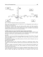
3. Principle of operation of an APD
The principle of operation of an Si APD, used in conjunction with PWO, or any other
scintillator emitting short wavelength light, which is strongly absorbed in Si, is illustrated
with the aid of Fig. 1. The basic elements of an APD are contained between the cathode and
anode contacts reversed biased with the positive potential on the cathode so that the wafer is
fully depleted. The electic field, reaching values as high as 2.5
·10
5
V/cm at the P-N junction,
as a function of depth is indicated schematically. The surface, through which the detected light
enters, is protected with an antireflective coating, Si
3
N
4
or SiO
2
, which improves the quantum
efficiency by reducing reflection losses from the surface of the Si wafer. The P-type material
in front of the amplification region, which forms the P-N junction (buried junction) is made
less than 7 μm thick to reduce sensitivity to the nuclear counter-effect. For e-h pairs generated
within the first few microns of the depletion layer, the electron is collected and undergoes
full multiplication, whereas for a pair generated within the wide drift region behind the
multiplying region only the hole enters the multiplying region, where it undergoes a much
reduced gain. This additional layer of N-type material is introduced to decrease the APD
capacitance and to improve stability with respect to changes in bias voltage. A notable feature
is the groove cut around thep-nstructure and slightly into the drift space (Deiters et al., 2000)
(not shown in Fig. 1) to limit the surface currents.
The nuclear counter-effect refers to the situation when the charged component (e
+
/e
−
)ofan
electromagnetic shower leaks out through the rear face of the scintillator and causes ionization
in the attached light sensor. This is an undesired effect, since it superimposes the signal
produced by scintillation light causing a decrease in its resolution. Comparing an APD with
277
Low-Energy Photon Detection with PWO-II Scintillators
and Avalanche Photodiodes in Application to High-Energy Gamma-Ray Calorimetry
Fig. 1. The concept of an Si APD intended for short-wavelength light detection is
demonstrated with a section of the Si wafer. The electric field distribution, E(x), is plotted
schematically to the left of the structure. Broken line marks the position of a P-N junction.
Note that relative thicknesses of the different regions are not shown in scale. Ar coating is an
abbreviation for Anti-reflective coating.
a PIN diode of the same thickness, one concludes that the nuclear counter-effect is very much
reduced in the former because of a narrow width of the collection region (see above).
4. Energy resolution of an APD in scintillation light detection
The performance of an APD depends on the number of primary electron-hole (e-h) pairs
produced by scintillation light, N
eh
, APD excess noise factor, F, and dark noise level of
the device-preamplifier system. The quantum efficiency,
Q
(λ), of the APD and spectral
distribution of the light emitted by a scintillator, N
phot
(λ), define the number of (e-h) pairs.
The excess noise is due to the statistical nature of the multiplication process, which causes
additional fluctuation of the measured signal. The excess noise factor depends on the ratio,
k
= β(E)/α(E), of ionization coefficients for electrons, α(E), and holes, β(E), both functions
of the electric field, E. F is a function of the internal structure of the diode, profile of the electric
field and the device operating gain. The statistical variance of the APD signal, σ
2
N
, is expressed
as:
σ
2
N
= M
2
σ
2
n
+ N
eh
σ
2
A
, (1)
where, σ
2
N
, is the variance of the output signal, expressed in the number of electrons, M,is
the APD gain, σ
2
n
is the variance of the number of primary electrons and σ
2
A
is the variance
of single electron gain. Dividing both sides of Eq. 1 with M
2
and taking into account the
definition of F:
F
= 1 + σ
2
A
/M
2
, (2)
we get the statistical variance of the signal from an APD, σ
2
st
:
σ
2
st
= σ
2
n
+ N
eh
(F − 1). (3)
278
Advances in Photodiodes
The first term in Eq. 3 corresponds to the statistical error of the detected signal, while the
second one to the contribution of the avalanche gain of an APD. Taking into account that σ
2
n
is
governed by Poisson statistics:
σ
2
n
= N
eh
, (4)
we find that the variance of APD signal is given by:
σ
2
st
= N
eh
F. (5)
Assuming that the detected peak is Gaussian and taking into account the relation between its
variance and full width at half maximum (FWHM), we may write that the FWHM resolution
is:
(ΔE)
2
=(2.36)
2
(N
eh
F + δ
2
noise
), (6)
where the dark noise contribution δ
noise
, expressed in rms electrons has been explicitely
included. One may rewrite Eq. 6 in energy units by taking into account that ε=3.6 eV is
required for one e-h pair creation in Si:
(ΔE)
2
=(2.36)
2
(FEε + Δ
2
noise
), (7)
where Δ
noise
is the dark noise contribution of the diode-preamplifier system (FWHM in energy
units). The relative energy resolution (in %) is:
ΔE/E
= 2.36(F/N
eh
+ δ
2
noise
/N
2
eh
)
1/2
. (8)
One may conclude from Eq. 8 that the relative energy resolution of the light signal is a
decreasing function of both the number of primary e-h pairs and the signal-to-noise ratio.
The high light output of a scintillator and high quantum efficiency of the employed APD are
of primary importance to reduce ΔE/E.
4.1 Dark noise contribution to energy resolution
The sources of dark noise in Eq. 6 are parallel and series noise of an APD. The parallel noise
originates from the surface and bulk dark currents of the device. The series noise is the effect
of shot noise of a preamplifier; it is proportional to the sum of APD capacitance and input
capacitance of preamplifier. Following Ref. (Lorenz et al., 1994) we may write δ
2
noise
in Eq. 6
as:
δ
2
noise
= 2q
I
ds
M
2
+ I
db
· F
τ + 4kTR
s
C
2
tot
M
2
1
τ
, (9)
where q is the electron charge, I
ds
the surface leakage current, I
db
the bulk current, τ the
shaping time constant of the amplifier (assumed τ
= τ
di f f
= τ
int
), k the Stephan-Boltzmann
constant, T the absolute temperature, R
s
the preamplifier series noise resistance, C
tot
the
parallel capacitance (APD plus preamplifier). We will show in Sect. 5 that APD capacitance
decreases rapidly with the reverse bias voltage.
Fig. 2 illustrates the dependence of the noise contribution vs. gain for different shaping time
constants of the amplifier. The measurements were performed in Ref. (Moszynski et al., 1997).
The lowest noise contribution is observed close to the maximum attained gain of 160 and the
shortest shaping time constant of 50 ns. Eq. 9 reflects the measured trends. The initial decrease
of noise with APD gain is related to a simultaneous action of several factors: the attenuation
of an unamplified noise component, related to I
ds
in Eq. 9, decreasing capacitance of the APD
with increasing bias voltage (see Fig. 3D) and the preamplifier noise. The curves have slightly
increasing tendency at high gain, passed the minimum, because of dark current excess noise
and fluctuations in avalanche gain, both of which increase with the excess noise factor,F.
279
Low-Energy Photon Detection with PWO-II Scintillators
and Avalanche Photodiodes in Application to High-Energy Gamma-Ray Calorimetry
Fig. 2. Noise (in rms electrons) as a function of the gain for different shaping time constants
measured in (Moszynski et al., 1997) [reproduced from (Moszynski et al., 2002) with permission of
Elsevier Ltd].
5. Main characteristics of Hamamatsu silicon APDs
The quantum efficiency of Hamamatsu APDs S8664-55/S8664-1010 as a function of light
wavelength is presented in Fig. 3A. One may see that at the wavelength of 420 nm,
corresponding to the maximum of PWO blue emission (see Table 1), the efficiency is above
70% and shows a broad plateau thereafter with an efficiency of about 85%. This should be
compared with about 18% of a typical photomultiplier with a bialkali photocathode in the
same spectral range. One may conclude that these APDs are very well matched for detection
of light from PWO. Light absorbed behind the P-N junction in Fig. 1 produces electrons and
holes, but only holes go to the avalanche region and multiply, while electrons drift towards
the back contact and are collected without multiplication. The multiplication factor for holes
is much smaller than that for electrons, as a result the gain for light with long wavelengths is
smaller than for short ones, which is reflected also as a drop with wavelength in Fig. 3A in the
quantum efficiency.
Fig. 3B presents plots of gain vs. reverse voltage at the different working temperatures. With
increasing voltage these curves approach the breakdown voltage, which is characterized by
an uncontrollable growth of the dark current (see Fig. 3C). On the other hand, the asymptotic
value of gain at low voltages is unity (not reached in Fig. 3B), at which carriers created in
the collection region are transferred though the p-n junction without multiplication. A typical
operating gain used with the indicated APDs is M=50 at room temperature, +20
◦
C. One may
note that decreasing the temperature down to -20
◦
C, which is close to the forseen operating
temperature of PANDA at -25
◦
C, will bring an increase of about a factor of 3 - 3.5 in gain.
This increase in gain is ascribed to decreasing excitation of lattice phonons, which permits
carriers to acquire higher energies used in avalanche multiplication. One may conclude that
both these operating parameters, voltage and temperature, should be carefully stabilized for
280
Advances in Photodiodes
Fig. 3. Selected characteristics of an APD S8664-1010 of Hamamatsu Photonics K.K. [by
courtesy of Hamamatsu Photonics K.K.].
a stable operation. The bias at room temperature cannot be chosen too high, because cooling
that follows, may end-up in break-down. M=50 is a safe initial choice, as proved in practice,
with the corresponding voltage and reverse current values at room temperature provided for
each APD by the producer. A further fine tuning of gain is accomplished by distributing a
reference light signal through a system of optical fibers in contact with an exit face of each
individual scintillator.
Comparing Hamamatsu Si-APDs with other producers, one notes several additional features
making the Japanese products more convenient in large-scale application, as in the
PANDA-EMC. The silicon wafer of S8664-1010 is installed on a thin ceramic plate, only
slightly exceeding in size the sensitive area 10
×10 mm
2
. Moreover, the surface through which
light enters is covered with a transparent plastics. This prevents from damaging the APD
upon exerting stress when a contact with the scintillator is done using an optical grease. Also,
much lower bias voltage at the same gain deserves stressing as a factor in favor of Hamamatsu
in large-scale applications.
281
Low-Energy Photon Detection with PWO-II Scintillators
and Avalanche Photodiodes in Application to High-Energy Gamma-Ray Calorimetry
6. Measurements of ΔE/E using high-energy tagged photon beams and detector
matrices
A comprehensive information on the performance of a PWO+APD combination is obtained
from an experiment in which the PWO scintillator is irradiated along its axis with a narrow
beam of photons and the scintillation light converted into an electronic signal with the aid of
an APD. It has been stressed in Sect. 2 that high-energy photons create an electron-positron
shower, which propagates both along and perpendicular to the scintillator axis. The lateral
dimensions of scintillators of about 20
× 20 mm
2
are determined by the required angular
resolution [granularity] in the forseen experiments (see (Erni et al., 2009)). With the Molière
radius (see Table 1) of 2.0 cm for PWO, one needs a matrix of at least nine closely packed
scintillators in order to intercept with the scintillating material and convert into light the
shower originating from the central one. An experiment using high-energy tagged photons is
illustrated in Fig. 4. Photons are products of bremsstrahlung of a high energy electron beam
from the MAMI-B microtron facility at Mainz in a thin carbon foil. There is a unique relation
between the energy of a photon and the momentum of an electron that it radiated, so that
the highest energy photons are accompanied with low-momentum electrons and vice-versa.
The post-radiation electron is bent in the magnetic field of a magnetic spectrometer and
detected with a position-sensitive detector along its focal plane. This illustrates the method
of photon-tagging with the aid of coincident electron detection in a certain range of positions
Fig. 4. Section of the magnetic spectrometer of the MAMI-B tagging facility along its central
plane. The iron flux return yoke is shown hatched. The dotted line is the trajectory of
electrons with the incident momentum. The solid lines are trajectories of electrons that
suffered bremsstrahlung with emission of photons with progressively increasing energy. The
matrix of nine PWO-II scintillators is located behind an iron collimator (not shown) with its
central scintillator axis along the photon beam [reproduced from (Anthony et al., 1991) with
permission of Elsevier Ltd].
in the focal plane (Anthony et al., 1991; Hall et al., 1996). In the experiment that we refer to
(Novotny et al., 2008) sixteen photon energies in the range 40.9 - 674.5 MeV were selected, and
282
Advances in Photodiodes
Fig. 5. Amplitude spectra illustrating the response of the central scintillator and the entire
3x3 PWO-II matrix, taken eventwise, to photons with E
γ
= 40.9 MeV selected with the MAMI
tagger. The matrix was kept at 0
◦
C[reproduced from (Novotny et al., 2008a)].
the primary electron beam energy was 840 MeV. Typical energy width per tagging channel
varied between 2.3 MeV at 50 MeV to 1.5 MeV at 500 MeV photon energy, respectively. The
matrix of 3x3 PWO-II scintillators was installed in a thermally isolated container, in which it
was cooled down to 0
◦
C. The container could be moved remotely in the plane perpendicular
to the photon beam, so that each of the nine scintillators could be inserted into the beam and
its amplitude spectra calibrated in energy at the sixteen points. After the calibration runs,
the central scintillator was inserted and the spectra in all of them simultaneously measured.
By summing eventwise the energy deposits, the energy response to a photon shower for the
entire matrix was determined. Fig. 5 compares the spectrum in the central scintillator with the
result of summing individual scintillator responses eventwise for the incident photon energy
E
γ
= 40.9 MeV. The summed spectrum is almost Gaussian, with only a slight indication of the
tailing seen. The reduced Gaussian widths, σ/E, of the summed peaks, are plotted in Fig. 6 as
a function of the photon energy. The solid line is a fit to the measured points with a formula:
σ
E
=
1.86%
E[GeV]
+
0.65%, (10)
where the energy is expressed in GeV. One recognizes here Eq. 8 with the first statistical, and
the second constant term. A comparison with the GEANT4 simulations (lower curve in Fig. 6),
which considers just the pure energy deposition into the scintillator material, demonstrates the
contribution due to photon statistics and the effect of experimental thresholds. The resolution
approaches asymptotically the simulation reflecting the decreasing relative importance of the
latter two factors. The value obtained by extrapolating Eq. 10 to 1.0 GeV is 2.5% - best
resolution ever measured at this energy for PWO with APD readout. One should stress that
energies lower than 40.9 MeV could not be reached with the MAMI photon tagger, having the
maximum photon energy set at 674.5 MeV, because of limitations imposed by the focal plane
detector.
283
Low-Energy Photon Detection with PWO-II Scintillators
and Avalanche Photodiodes in Application to High-Energy Gamma-Ray Calorimetry